
 Open Access Article
 This Open Access Article is licensed under a
 Creative Commons Attribution 3.0 Unported Licence
Thermal properties of metal-halide perovskites
Tobias
Haeger
a,
Ralf
Heiderhoff
 *ab and
Thomas
Riedl
ab
*ab and
Thomas
Riedl
ab
aInstitute of Electronic Devices, University of Wuppertal, Wuppertal, Germany. E-mail: heiderho@uni-wuppertal.de
bWuppertal Center for Smart Materials & Systems, University of Wuppertal, Wuppertal, Germany
First published on 7th September 2020
Abstract
Aside from photovoltaics, metal-halide perovskite semiconductors have also emerged as an attractive platform for LEDs and even lasers. For all of them, performance and operational stability are strongly influenced by thermally activated processes. As a result, studying the thermal properties of halide perovskites has become increasingly important. In addition to thermal conductivity measurements, thermal diffusivity and heat capacity studies are becoming more and more relevant for the dynamic operation of these devices. Here, we will review the current state of knowledge on the thermal properties of metal halide perovskites, including both experimental findings and theoretical insights. We will highlight the impact of the perovskite dimensionality (3D, 2D, 0D) on the thermal properties and how these properties change across the various phase transitions of these perovskites. Our review will also discuss thermal measurement methods, which can be favourably used to determine the thermal properties of both bulk and thin film samples. Advanced comprehensive tools and strategies for systematic thermal analyses and property optimizations are discussed.
 Tobias Haeger | Tobias Haeger received his BSc and MSc degrees in electrical engineering from the University of Wuppertal, Germany, in 2015 and 2017, respectively. Since 2017 he has been a PhD Student at the Chair of Electronic Devices. His major research is focused on thermal measurements, especially scanning thermal microscopy (SThM) as well as the production and characterization of all-inorganic/hybrid perovskite thin films and single crystals. |
 Ralf Heiderhoff | Dr-Ing. Ralf Heiderhoff studied physics and he got his doctoral degree from the Faculty of Electrical, Information, and Media Engineering at the University of Wuppertal (1997). In 1999 he was Visiting Lecturer at the National University of Singapore followed by a Visiting Professorship at the Belarusian State University of Informatics and Radioelectronics (2001) and at the Beijing University of Technology (2008). His major research is focused on electrical, opto-electronic, micromechanical, and thermal measurements in the nanometer range as well as the combination of Scanning Electron Microscopes and Scanning Probe Microscopes to form hybrid systems. |
 Thomas Riedl | Thomas Riedl received his PhD (Dr rer.-nat.) degree in physics from the Technical University of Braunschweig, Germany, in 2002. From 2002 to 2009, he was an Akademischer Oberrat (Lecturer) at the Institute of High Frequency Technology, Technical University of Braunschweig, heading the Advanced Semiconductors Group. Since 2009 he has been full professor (W3) at the University of Wuppertal and Chair of Electronic Devices. He is director of the Wuppertal Center for Smart Materials & Systems, an interdisciplinary research center at the University of Wuppertal. His research interests include organic/hybrid (opto-)electronic devices, and the fundamental properties of organic/inorganic hybrid interfaces. |
Introduction
The perovskite structure, in its crystal form ABX3,1 allows for a wide range of materials with entirely different physical properties that unlock a plethora of functionalities.2 In the past, in addition to piezoelectric, ferroelectric and related applications, perovskites have received particular attention in superconductivity.3 Semiconducting properties were reported for caesium-lead-halide perovskites in 1958.4 Following this work, the A-site cation was replaced with an organic cation such as CH3NH3 (methylammonium: MA) to form CH3NH3PbX3.5The outstanding (opto-)electronic properties of these lead-halide perovskites have been re-discovered during the past decade. Most impressively, the power conversion efficiency of lab-scale perovskite solar cells (PSCs) has rapidly increased to a level of 25.2%,6 which rivals that of crystalline silicon. In addition, a wide range of other applications such as light emitting diodes (LEDs)7 and lasers8,9 have been explored. Moreover, this family of materials also holds great promise for thermoelectric generators.10 Here, the extremely low thermal conductivities of lead-halide perovskites11,12 may be advantageous, while for the vast majority of opto-electronic devices heat transfer may be an issue and thermal management requires particular attention. It is known that the crystalline structure of some representatives undergoes phase transitions T slightly above room temperature (RT); for example, CsPbCl3 is in the tetragonal phase at RT, whereas above 46.9 °C it becomes cubic.13 At early times high coefficients of thermal expansion were reported.14 Both the crystalline phase and thermal expansion influence electronic properties (for instance, carrier mobility, directionality) and carrier dynamics.15 More severely, substantial decomposition effects for MA-based perovskites have been found to occur already below 100 °C even in an inert atmosphere.16 Consequently, heating as a result of a lack of thermal management may turn out detrimental in various aspects.17–20 This holds particularly for (concentrator) solar cells and LEDs and the prospects of electrically or continuous wave operated perovskite lasers.21,22
Thus, in a wide range of these organic–inorganic and all-inorganic perovskites, the acquisition of extreme thermal properties has become more and more important, because both the lifetime and performance are influenced by temperature or temperature gradients.23,24 As detailed in the following, considerable research efforts have provided access to thermo-elastic and thermo-electric properties, as well as to intrinsic thermal conductivities, thermal diffusivities, and heat capacities.
It is important to note that thermal properties strongly depend on temperature themselves and phase transitions may cause significant and abrupt changes. By a similar token, the thermal properties of 0D and 2D materials may significantly differ from those of the bulk (3D).
In the following sections we will review the thermal properties of metal-halide perovskites and the experimental techniques that have been used to assess them. The experimental data will be complemented by the results of theoretical work that is indispensable to understand the particular thermal properties of this class of materials and to identify levers to overcome limitations.
Heat dissipation in metal-halide perovskites
Although a heat spreading in steady state photovoltaics and thermo-electrics is often directly related to the thermal conductivity λ(![[r with combining right harpoon above (vector)]](https://www.rsc.org/images/entities/i_char_0072_20d1.gif) ) (note: λ() is a tensor) of the metal-halide perovskite semiconductor used,25 its specific heat csp() and thermal diffusivity a() must be considered for dynamic (transient) heat transport in a wide range of applications. The volumetric heat capacity cvol.(), which is the product of csp() and the density ρ() of the material, describes the capability to store heat. The thermal diffusivity a(), which can only be simplified in homogeneous and isotropic materials to a() = λ()/cvol.(), denotes the ability of a material to conduct thermal energy relative to its ability to store thermal energy. Consequently, the temperature distribution T() in perovskite devices depends on the local amount of heat generated per unit volume qE(). T() is described by the general equation of heat conduction, i.e., the classical Fourier law:26,27
) (note: λ() is a tensor) of the metal-halide perovskite semiconductor used,25 its specific heat csp() and thermal diffusivity a() must be considered for dynamic (transient) heat transport in a wide range of applications. The volumetric heat capacity cvol.(), which is the product of csp() and the density ρ() of the material, describes the capability to store heat. The thermal diffusivity a(), which can only be simplified in homogeneous and isotropic materials to a() = λ()/cvol.(), denotes the ability of a material to conduct thermal energy relative to its ability to store thermal energy. Consequently, the temperature distribution T() in perovskite devices depends on the local amount of heat generated per unit volume qE(). T() is described by the general equation of heat conduction, i.e., the classical Fourier law:26,27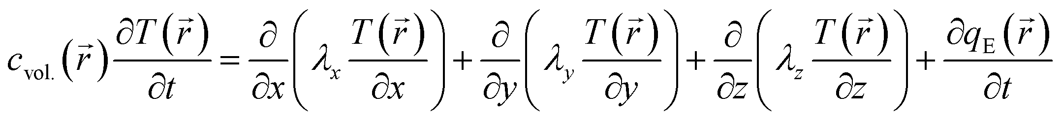 | (1) |
) and cvol.() are given by electronic and phononic/lattice contributions. Note that the thermal conductivities are related to the heat capacities through the Drude model relationship28 and the phonon gas model,29 respectively. In a certain way they can be correlated with the electrical conductivity by the Wiedemann–Franz law as well as with the activated volumetric phonon heat capacity, the average phonon group velocity, and the average phonon mean-free path of the metal-halide perovskite semiconductor used.30 More accurately, the dispersion relations of electrons and phonons must be considered to obtain further insights.31 The reduced group velocity of phonons, due to band flattening in the phonon dispersion, and phonon scattering at grain boundaries are primarily responsible for the ultralow thermal conductivities in metal-halide perovskites (see Fig. 1).32
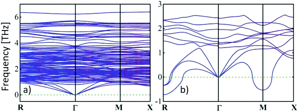 | ||
| Fig. 1 An ultralow thermal conductivity can be obtained from the calculated phonon dispersion curves in the low-frequency domain of (a) tetragonal MAPbI3 at room temperature, while the thermal conductivity of (b) the cubic phase (>54 °C33) is slightly larger, because the phonon group velocities are given by the gradient.31 Copyright Wiley-VCH Verlag GmbH & Co. KGaA. Reproduced with permission. | ||
Only their absolute group velocities, mean-free paths, and lifetimes obtained from these relations in all directions provide access to the anisotropy of thermal transport. In addition, the phonon dispersion is essential for the description of heat dissipation in the temperature-dependent crystalline structure and the dimensionality given by its composition AxByXz in these perovskite semiconductor types.
The electron/phonon heat capacity can be calculated by taking the derivative of the total electron/phonon energy density with respect to the electron/phonon temperature: in other words, the amount of heat, ΔQ(), that must be added to a system in order to increase its temperature by ΔT(). A first-order phase transition in a crystalline structure is described by the Clausius–Clapeyron equation. This results in the divergence of the heat capacity csp(T) or the thermal expansion coefficient α(T), because the first derivative of the free energy is discontinuous. In contrast, a second-order (continuous) phase transition, which is described by the Ehrenfest equation, occurs with diverging correlation length as the crystalline phase transition temperature is approached. For material systems undergoing this phase transition due to continuous entropy changes such as magnetic and ferroelectric, the latent heat is zero, and no discontinuity in csp(T) and α(T) occurs.
Thus, the detection of the thermal properties λ, csp, cvol., a, and α depending on their temperature is challenging, because comprehensive thermal studies allow access to a variety of material properties and are indispensable for the heat management of semiconducting perovskite devices.
Molecular dynamics calculation
Only a few equilibrium molecular dynamics simulations (MDS) have been performed to understand the temperature-dependent phonon dispersion in organic–inorganic perovskites and in their inorganic counterparts.31,34–38 First calculations already demonstrated that with the aid of phonon group velocity, phonon lifetime, and normal mode analysis, these simulations provide a thorough explanation for the fundamental mechanisms underlying the ultralow thermal conductivity.34 Since details of steady state thermal transport in halide perovskites depending on their thermal conductivities, their dependency on the chemical composition, and some of their intriguing phonon characteristics have been excellently reviewed elsewhere,25 molecular dynamics calculations are only briefly addressed here.A very low thermal conductivity of 0.59 W (m K)−1 was found in the tetragonal phase at room temperature of MAPbI3, attributed to the low group velocity of acoustic phonons due to their low elastic stiffness and the strong anharmonicity, whereas a much higher thermal conductivity was predicted for the pseudo-cubic phase (1.80 W (m K)−1 at 57 °C).35 It was argued that the lower thermal conductivity in the tetragonal phase was due to the shorter lifetimes of the optical phonons and the smaller group velocity of acoustic phonons than those in the pseudo-cubic phase. In addition, the thermal conductivity of MAPbI3 was predicted to be below 1 W (m K)−1, and as low as 0.31 W (m K)−1 at room temperature.31 Such ultralow thermal conductivity, as a result of the enhanced phonon–phonon scattering from highly-overlapped phonon branches, hints to short phonon lifetimes <100 ps and consequently short phonon mean-free paths <10 nm. Compared with FAPbI3, a 3 times higher carrier-phonon relaxation rate is observed, while that in a cesium-based system is 10 times higher.36 In general, the thermal conductivities of lead-based perovskites are low, due to the low sound velocity of the PbX lattice.37 In this context it should be noted that the contribution of the average phonon group velocity to the thermal conductivity has been discussed elsewhere.30 Nevertheless, the degrees of freedom of the A-site cation also provide a route to tune λ.
Hence the role of the rotations of MA+ cations in thermal properties has been studied by molecular dynamics simulations in addition.38 The vibrational energy shifts as the temperature increases, where anharmonic couplings occur. Coupled translational and rotational motions of CH3NH3+ were found to interact with the Pb–I cages and afford couplings between the isolated lattice vibrations, which suppress the phonon transport in MAPbI3.
The anisotropy in the tensor of thermal conductivity  for the tetragonal and orthorhombic phases was found to originate from the preferential orientations of MA+.31 It has been claimed that among all the atomistic interactions, electrostatic interactions dominate thermal conductivity in ionic MAPbI3 crystals. Hence, hybrid perovskites are sometimes also considered as “soft materials”.
Recent MDS show that the A-site component of two-dimensional metal halide perovskites induces a reduction of the stiffness and sound velocities along with giving rise to vibrational modes in the 5–15 THz range that are absent in the three-dimensional counterparts.32 This leads to ultralow thermal conductivities in the range of 0.10 to 0.19 W (m K)−1 depending on the molecular substructure of ammonium cations and owing to the weaker interactions in the layered structures.
Thermal transport investigations of perovskite alloys in particular, which have been successfully developed to design various layered structures,39,40 have been performed rarely, with the first reports published just recently.41–43 The electrical behavior, optical absorption, and heat conduction or convection are considered to give insight into heat dissipation across solar cells. These first inspections of heat accumulations and gradients in transparent front electrode and back electrode materials are promising for the higher thermal stabilities of these devices, since they also take the heat dissipation in air into account.
Note that dynamical heat transport analyses have not been carried out so far. Accordingly, their experimental thermal property studies for reliable dynamic device operation will be considered in addition in the following.
Experimental determination of thermal properties
Even though interest in heat transport in metal-halide perovskites has become increasingly important in recent years with emerging applications in devices, numerous experimental studies have been devoted to their thermal properties already in the past. Their content and the results achieved will briefly be summarized in the following. The detailed values of the thermal quantities found are summarized in Table 1.| Perovskite | SC/PC | λ [W (m K)−1] | c s [J (kg K)−1] | c V [MJ (m3 K)−1] | a [mm2 s−1] |
![[v with combining macron]](https://www.rsc.org/images/entities/i_char_0076_0304.gif) s [m s−1]
s [m s−1] |
S [μV K−1] | Measurement technique | Measured [K] | Crystal phase | Perovskite manufacturing | Year | Ref. |
|---|---|---|---|---|---|---|---|---|---|---|---|---|---|
| MAPbI3 | SC | 0.5 | Steady-state method | RT | Tetragonal | ITC | 2014 | 12 | |||||
| MAPbI3 | SC | 0.31 or <1 for all phases | Molecular dynamics simulation | RT | Orthorhombic, tetragonal, cubic | 2016 | 31 | ||||||
| MAPbI3 | SC | 0.30–0.42 (i) | 920 ± 91 | Laser flash | 298–425 | Tetragonal–cubic | ITC/vapor diffusion | 2017 | 59 | ||||
| MAPbI3 | SC | 0.34 ± 0.12 | SThM/3ω method | RT-313 | Tetragonal | ITC | 2017 | 61 | |||||
| MAPbI3 | SC | 0.14 ± 0.02 | Micro-photoluminescence | RT | Tetragonal | Two-step CVD grown | 2017 | 220 | |||||
| MAPbI3 | SC | 0.34 ± 0.08 | 311 calculated | 1.28221 | 0.28 calculated | 1390+43−66 | Frequency domain thermo-reflectance | RT | Tetragonal | Vapor diffusion | 2017 | 30 | |
| MAPbI3 | SC | 0.59 | Molecular dynamics simulation | 160–330 | Tetragonal | 2016 | 35 | ||||||
| MAPbI3 | SC | 1.8 | Molecular dynamics simulation | >330 | Pseudocubic | 2016 | 35 | ||||||
| MAPbI3 | SC | 0.30 | Laser flash | RT | Tetragonal | ITC | 2018 | 63 | |||||
| MAPbI3 | SC-NW | 0.22 | Microbridge – device | RT | Tetragonal | 222 | 2018 | 49 | |||||
| MAPbI3 | PC | 0.6 | Longitudinal steady state technique | RT | Vacuum quenching | 2017 | 53 | ||||||
| MAPbI3 | PC | 0.33 ± 0.12 | SThM/3ω method | RT-318 | Tetragonal | Spincoating/NIL | 2017 | 61 | |||||
| MAPbI3 | PC | 0.3 | Steady-state method | RT | Tetragonal | ITC/glueing | 2014 | 12 | |||||
| MAPbI3 | PC | 11.2 ± 0.8 | Time-domain thermal reflectance | RT | Tetragonal | 223 | 2016 | 62 | |||||
| MAPbI3 | PC | 0.38 | 1350 ± 50 | Laser flash | 300–450 K | Tetragonal cubic | Mechanical alloying via high energy ball milling, followed by hot pressing | 2019 | 76 | ||||
| MAPbI3 | PC | 0.36 ± 0.01 | Laser flash | 300 K | Tetragonal | — | 2019 | 77 | |||||
| MAPbI3 | PC | 0.32 ± 0.03 | 6500/5500 | 3ω method | RT | Tetragonal | Two-step sequential vacuum | 2019 | 224 | ||||
| Deposition | |||||||||||||
| SVD | |||||||||||||
| MAPbI3 | PC | 0.31 ± 0.03 for film thicknesses 65 ± 3 nm | 3ω method | RT | Coevaporation | 2019 | 225 | ||||||
| MAPbI3 | PC | 0.44 ± 0.03 for film thicknesses 80 ± 5 nm | 3ω method | RT | Coevaporation | 2019 | 225 | ||||||
| MAPbI3 | PC | 0.59 ± 0.04 for film thicknesses 100 ± 12 nm | 3ω method | RT | Coevaporation | 2019 | 225 | ||||||
| MAPbI3 | PC | 820 (dark) | ITC | 2015 | 56 | ||||||||
| 540 (light) | |||||||||||||
| MAPbI3 | PC | Average 0.4 | 1.200 ± 300 | TDTR | RT | Spincoating | 2016 | 60 | |||||
| MAPbBr3 | SC | 0.44 ± 0.08 | SThM/3ω method | RT | ITC | 2017 | 61 | ||||||
| MAPbBr3 | SC | 0.51 ± 0.12 | 378 calculated | 1.45221 | 0.35 calculated | 1717+79−1216 | Frequency domain thermo-reflectance | RT | Cubic | Vapor diffusion | 2017 | 30 | |
| MAPbBr3 | SC | 0.37 | Laser flash | RT | Cubic | ITC | 2018 | 63 | |||||
| MAPbBr3 | SC-NW | 0.32 | Microbridge – device | RT | Cubic | 222 | 2018 | 49 | |||||
| MAPbBr3 | PC | 0.39 ± 0.05 | SThM/3ω method | RT | Spincoating/NIL | 2017 | 61 | ||||||
| MAPbCl3 | SC | 0.73 ± 0.18 | 511 calculated | 1.62221 | 0.45 calculated | 2194+71−108 | Frequency domain thermo-reflectance | RT | Cubic | Vapor diffusion | 2017 | 30 | |
| MAPbCl3 | SC | 0.50 ± 0.05 | SThM/3ω method | RT | ITC | 2017 | 61 | ||||||
| MAPbCl3 | SC | 0.52 | Laser flash | RT | Cubic | ITC | 2018 | 63 | |||||
| MAPbCl3 | PC | 0.50 ± 0.12 | SThM/3ω method | RT | Spincoating/NIL | 2017 | 61 | ||||||
| CsPbI3 | SC-NW | 0.45 ± 0.05 (κl) | NW thermometry technique | RT | — | 2017 | 48 | ||||||
| CsPbBr3 | PC | 0.43 ± 0.03 | 290 ± 90 calculated | 1.3 ± 0.4 | 0.3 ± 0.1 | SThM/3ω method | RT | Orthorhombic | Spincoating/NIL | 2019 | 50 | ||
| CsPbBr3 | SC | 0.46 ± 0.12 | 220 calculated | 1.06 | 0.43 calculated | 1390+96−74 | Frequency domain thermo-reflectance | RT | Orthorhombic | Vapor diffusion | 2017 | 30 | |
| CsPbBr3 | SC | 0.514 | 280 | 1.29 calculated | 0.399 | Pulse transient method | 37 °C | 2008 | 217 | ||||
| CsPbBr3 | SC-NW | 0.36 | Microbridge – device | RT | Orthorhombic | 222 | 2018 | 49 | |||||
| CsPbBr3 | SC-NW | 0.42 ± 0.04 (κl) | NW thermometry technique | RT | — | 2017 | 48 | ||||||
| CsPbCl3 | SC | 0.530 | 272 | 1.12 calculated | 0.475 | Pulse transient method | 25 °C | 226 | 2008 | 217 | |||
| CsPbCl3 | SC | 0.55 ± 0.03 | 272 ± 8 | 1.143 calculated | 0.49 ± 0.02 | Pulse transient method | 50 °C | 226 | 2000 | 11 | |||
| CsPbCl3 | PC | 0.49 ± 0.04 | 220 ± 70 calculated | 0.9 ± 0.1 | 0.5 ± 0.1 | SThM/3ω method | RT | Monoclinic | Spincoating/NIL | 2020 | 51 | ||
| FAPbBr3 | SC | 0.49 ± 0.12 | 444 calculated | 1.69 | 0.29 calculated | 1333+51−73 | Frequency domain thermo-reflectance | RT | Cubic | Vapor diffusion | 2017 | 30 | |
| MASnI3 | PC | 0.09 | −720 | Steady state method | ITC | 2015 | 56 | ||||||
| CsSnI3 | SC-NW | 0.38 ± 0.04 (κl) | NW thermometry technique | RT | — | 2017 | 48 | ||||||
| CsSnI3 | SC-NW | 0.57 | 79 | NW thermometry technique | 300 K | — | 2017 | 48 | |||||
| CsSnI3 | PC | 0.36 | 115 | 3ω method | RT | Spincoating | 2020 | 70 | |||||
| (MA)3Bi2I9 | PC | 0.21 | 2600 ± 200 | Laser flash | 300–450 K | Mechanical alloying via high energy ball milling, followed by hot pressing | 2019 | 76 | |||||
| (MA)3Bi2I9 | PC | 0.23 ± 0.02 | Laser flash | 300 K | — | 2019 | 77 | ||||||
| Cs0.05FA0.95Pb(I0.83Br0.17)3 | PC | 0.26 ± 0.03 | 0.74 ± 0.11 calculated | 0.35 ± 0.05 | Thermo-reflectance | RT | Spincoating | 2020 | 85 | ||||
| Low-dimensional perovskites | |||||||||||||
| [Mn(C2H6OS)6]I4 | SC | 0.15 ± 0.01 | 580 ± 20 | 0.12 ± 0.01 | Laser flash differential calorimeter | RT | ITC | 2019 | 214 | ||||
| CsPb2Br5 | PC | 0.33 ± 0.02 | 180 ± 60 calculated | 1.1 ± 0.3 | 0.3 ± 0.1 | SThM/3ω method | RT | Spincoating/NIL | 2019 | 50 | |||
| CsPb2Cl5 | PC | 0.40 ± 0.02 | 0.7 ± 0.2 | 0.6 ± 0.1 | SThM/3ω method | RT | Spincoating/NIL | 2019 | 215 | ||||
| Cs4PbCl6 | PC | 0.30 ± 0.03 | 150 ± 80 calculated | 0.5 ± 0.2 | 0.5 ± 0.1 | SThM/3ω method | RT | Spincoating/NIL | 2020 | 51 | |||
| BA2PbI4 | PC | 0.10 ± 0.02 horizontal | 1.22 horizontal | Thermo-reflectance molecular dynamics simulation | RT | Spincoating | 2020 | 32 | |||||
| 0.18 ± 0.04 vertical | 1.18 vertical | ||||||||||||
| BA2PbBr4 | PC | 0.11 ± 0.02 horizontal | 1.37 horizontal | Thermo-reflectance molecular dynamics simulation | RT | Spincoating | 2020 | 32 | |||||
| 0.19 ± 0.04 vertical | 1.37 vertical | ||||||||||||
| PEAPbI4 | PC | 0.15 ± 0.03 | 1.19 | Thermo-reflectance molecular dynamics simulation | RT | Spincoating | 2020 | 32 | |||||
| PEAPbBr4 | PC | 0.13 ± 0.03 | 1.22 | Thermo-reflectance molecular dynamics simulation | RT | Spincoating | 2020 | 32 | |||||
| BA2MA3 | PC | 0.13 ± 0.03 vertical | Thermo-reflectance | RT | Spincoating | 2020 | 32 | ||||||
| Pb4I13 | 0.11 ± 0.03 random | ||||||||||||
The first detailed thermo-mechanical experimental investigations of both CsPbCl3 and CsPbBr3 perovskites were made in the 1970s in order to understand the nature of their structural phase transitions.44–47 But the corresponding specific heat csp and thermal diffusivity a values of the different phases as well at their transitions were obtained in transient measurements on single crystals much later (which will be discussed in more detail later in the Thermal properties across phase transitions section).11 In addition, thermal conductivity studies have been carried out for all-inorganic halide perovskite nanowires, CsPbI3 and CsPbBr3.48,49 The authors generally concluded that nanostructures or crystal grains with dimensions smaller than 100 nm significantly reduce the thermal transport because phonons have a mean-free path on the same order. Thus, somewhat higher thermal conductivities are reported for CsPbBr3 single crystals (0.46 W (m K)−1)30 and thin films containing large crystals (0.43 W (m K)−1)50 in comparison to nanowires (0.36 W (m K)−1).49 These thermal conductivities are somewhat lower than those recently found for CsPbCl3 thin films with large laterally extended crystallites (0.49 W (m K)−1).51 Note that, since the phonon mean-free-path is also reduced by defects, thermal conductivities are lower near grain boundaries in thin films, as shown in local thermal conductivity analyses with a high spatial resolution by an AFM based technique.50 This technique allows determining the local thermal diffusivity, aside from the local thermal conductivity; thus the local volumetric heat capacity can be calculated afterwards. Average a() of 0.3 mm2 s−1 and 0.5 mm2 s−1 as well as average cvol.() of 1.3 J cm−3 K−1 and 0.9 J cm−3 K−1 were determined for CsPbBr3 and CsPbCl3 at RT respectively.50,51
The findings of these studies suggested that heat dissipation in dynamically operated halide perovskite optoelectronic devices will be very inefficient. As such, the thermal management of light-emitting diodes and lasers based on halide perovskites is a challenge and requires particular attention (see strategies to enhance the thermal properties of transport layers in perovskite devices).
The specific heat capacities of MAPbX3 (X = I, Br, and Cl) perovskites were studied by Onoda-Yamamuro et al. in 1990 to be 19.0 J (K mol)−1, 8.2 J (K mol)−1, and 10.0 J (K mol)−1 at RT for X = I, Br, and Cl, respectively.52 Upon heating the MAPbI3 samples above room temperature, a tetragonal to pseudo-cubic polymorph transition (57 °C) was observed that led to a reduction of csp to 9.7 J (K mol)−1. Pisoni et al. performed the first thermal conductivity measurements of MAPbI3 for temperatures below RT.12 The analysis was performed by a steady state bar technique. The room temperature thermal conductivity λ was determined to be 0.5 W (m K)−1 and 0.3 W (m K)−1 for a single crystal and a polycrystalline sample, respectively. The same thermal conductivity was found for a polycrystalline sample when measuring the effect of the methylammonium ion on phonon scattering.53 The low thermal conductivity of the MAPbI3 single crystal was mainly attributed to the rotational motion of the MA cations54 and has attracted intense attention due to its possible thermoelectric applications.55 A high Seebeck coefficient S of 0.82 mV K−1,56 a decent charge carrier mobility in the range of 5–10 cm2 (V s)−1 for electrons and 1–5 cm2 (V s)−1 for holes,57 and a high carrier diffusion length >1 μm58 were reported. The thermal conductivity of a MAPbI3 perovskite was also evaluated using laser flash systems. Values of around 0.30–0.42 W (m K)−1 were observed for a single crystal in the temperature range of RT to 150 °C.59 Similar values were found for films using the time-domain thermo-reflectance (TDTR) method.60 In striking contrast to all other reports, an extremely high thermal conductivity of densely packed MAPbI3 films of 11.2 ± 0.8 W (m K)−1 at room temperature was claimed by Chen et al.62
On the other hand, consistent thermal conductivities were reported for single crystals (0.34 W (m K)−1) and densely packed thin perovskite films containing large crystals (0.33 W (m K)−1) using 3ω-scanning near-field thermal microscopy.61 In addition, the temperature-dependent thermal conductivity of MAPbI3 was first measured around the tetragonal–cubic phase transition temperature. It could be demonstrated that the thermal conductivity of a cleaved single crystal in the cubic structure increases to 1.1 W (m K)−1, in excellent agreement with the results of EMD simulations,31 which, however, could not be verified from other heat transport measurements.63 Furthermore, it could experimentally be shown that MAPbX3 (X = I, Br, and Cl) single crystals and thin films with the decreasing atomic number of the halide show a slightly increasing average thermal conductivity due to their significantly increasing elastic stiffness (see Fig. 2).30,61 Besides the above mentioned halide variations, studies have been carried out on FAPbBr3,30 on targeted thermo-electrics such as CsSnI3,48,70–72 and on estimated lead-free solid-state organic–inorganic halide perovskite solar cell materials such as MASnI373,74 and (MA)3Bi2I9,75,76 with which the influences of A- and B-cation substitutions on thermal transports were examined (see Fig. 3).
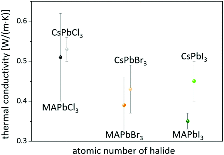 | ||
| Fig. 2 Perovskites with the decreasing atomic number of the halide have slightly higher average thermal conductivities.30,61 | ||
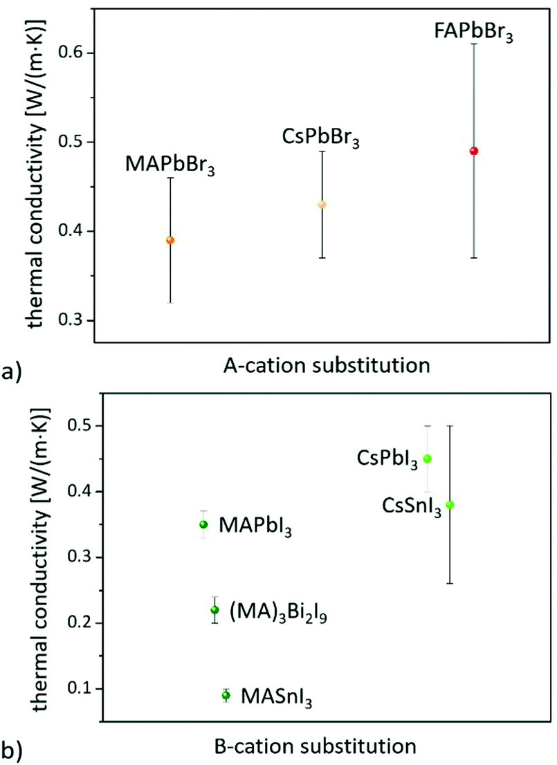 | ||
| Fig. 3 The influence of (a) A- and (b) B-cation substitutions on thermal transports. | ||
The obtained λ values of 0.74–0.28 W (m K)−1 for CsSnI3 vary significantly for single crystals, nanowires, and polycrystalline films due to the enhanced phonon scattering by defects/vacancies and reduced crystal sizes. Polycrystalline MASnI3 seems to have a glassy behavior, which might be the reason for its ultralow thermal conductivity of 0.09 W (m K)−1.74 Lastly, it must be pointed out that the thermal properties of 0D and 2D perovskite materials significantly differ from those of the bulk (3D). 0D Bi based perovskites, for instance, have a lower thermal conductivity of 0.21 W (m K)−1 than Pb based systems, which is due to their soft phonon dispersion and weak bonds.77 Since these materials can also be useful for a wide range of applications,78 the Dimensionalities of metal-halide perovskites section will highlight their impact on thermal transport.
In summary, the mean values of thermal properties obtained from molecular dynamics calculations and experimental investigations of representative studies are listed in Table 2. This table is intended to provide an overview for the assessment of a suitable thermal management of halide perovskite devices, since these properties of these compounds are very different from those of other materials. For example, thermally insulating materials commonly have large heat capacities, whereas those with high thermal conductivities, such as metals, have low ones. Thus, afterwards, thermal measurement methods used will also be discussed briefly with regard to their applicability to determine these very low thermal quantities of both bulk and thin film samples. Advanced comprehensive tools for systematic thermal analyses are highlighted in this context.
| Material | λ [W (m K)−1] | a [mm2 s−1] | C s [J (g K)−1] | C v [J (cm3 K)−1] |
s [m s−1] |
|---|---|---|---|---|---|
| MAPbI3 | 0.35 ± 0.02 | 0.28 ± 0.07 | 0.31 ± 0.08 | 1.28 | 1295 ± 134.35 |
| MAPbBr3 | 0.39 ± 0.07 | 0.35 ± 0.08 | 0.38 ± 0.09 | 1.45 | 1717+79−126 |
| MAPbCl3 | 0.51 ± 0.11 | 0.45 ± 0.09 | 0.51 ± 0.13 | 1.62 | 2194+71−108 |
| CsPbI3 | 0.45 ± 0.05 | — | — | — | — |
| CsPbBr3 | 0.43 ± 0.06 | 0.40 ± 0.07 | 0.28 ± 0.04 | 1.29 ± 0.14 | 1361+74−96 |
| CsPbCl3 | 0.53 ± 0.03 | 0.49 ± 0.01 | 0.27 ± 0.03 | 1.12 ± 0.13 | — |
| Si | 15664 | 78 | 0.765 | 1.6 | 8500 |
| GaAs | 4564 | 26 | 0.3366 | 1.7 | 5300 |
| CZTS | 4.7267 | 2067 | 0.0567 | 0.24 | — |
| CZTSe | 4.2667 | 2067 | 0.0467 | 0.21 | — |
| Organic | 0.368 | 0.15 | 1.7 | 269 | — |
Thermal measurement methods
Today, the development of new thermal characterization techniques for electronic materials is underway, which has been reviewed with respect to their application elsewhere.79 So far, however, only a few of these enhanced thermal measurement methods mostly developed for failure analyses and reliability investigations in microelectronics have been applied to study thermal transport in halide perovskite-based systems. Rather, thermal analysis tools are used which will be briefly summarized in the following.The common theoretical framework of these methods is based on the Fourier law:26,27
![[q with combining right harpoon above (vector)]](https://www.rsc.org/images/entities/i_char_0071_20d1.gif) = −λ·grad = −λ·grad![[thin space (1/6-em)]](https://www.rsc.org/images/entities/char_2009.gif) T() T() | (2) |
in thin films and bulk samples is classically described as normal diffusive transport for a given temperature distribution, T(). The techniques used so far for thermal property measurements of halide perovskites can be divided into two main categories: steady-state techniques and transient techniques. For the former, the thermal conductivity can be directly determined from eqn (2), if the absorbed power in the sample is known. For the latter, the specific density as well as the specific heat of the material must be considered, and the heat flow is described by the general equation of heat conduction (see eqn (1)).
The steady-state measurement technique can be described in the simplest way by the thermal characterization based on the analysis in space. The schematic of a thermal resistivity measurement setup in a standard four-point configuration is shown in Fig. 4. An electrical heater, where () is equal to the electrical power, is connected to a sample, represented by the black rectangle, using epoxy. The sample is connected to a calibrated reference material, which is glued to a heat sink for heat dissipation. The given temperature distribution is obtained using differential thermocouples fixed onto the sample and onto the reference surfaces to determine the thermal conductivity. This common technique was the very first one introduced to determine the thermal conductivity of materials and has been improved successively.80,81 Of course, it must be ensured that the thermal measurement itself does not lead to artifacts. For instance, the experiments must be carried out in the dark to avoid unwanted photo-induced effects. Special care must be taken in the case of polycrystalline perovskite structures, as the thermal transport is significantly influenced by the presence of many grain boundaries. Thus, large single crystal perovskites are initially preferred in order to explore the thermal properties in detail. Furthermore, solvents of glues used to mount heaters or thermocouples to the sample may cause degradation.
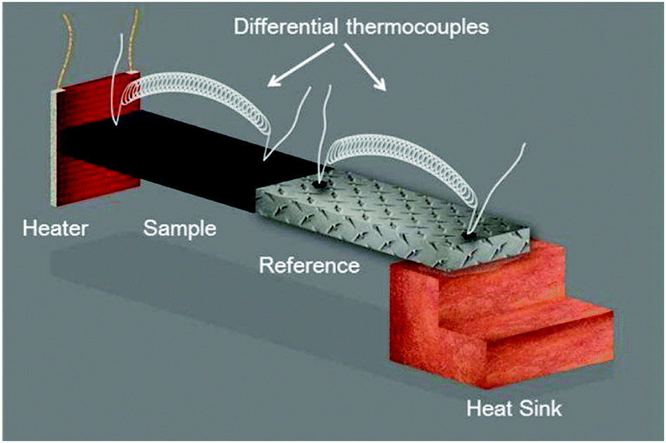 | ||
| Fig. 4 Schematic of a thermal resistivity measurement setup in a standard four-point configuration. Reprinted with permission from ref. 12. Copyright (2014) American Chemical Society. | ||
Thus, a non-contact optical flash method was already established in 1961,82 which is widely used in commercial thermal conductivity measurement systems. Its application to the study of microelectronic materials by the detection of thermal waves through changes in their optical reflectance was primarily demonstrated in 1985.83 The initial thermal diffusivity measurements of thin films by means of an AC calorimetric method were performed in the same year.84 Similar to these analyses, a modulated thermo-reflectance microscopy technique (shown in Fig. 5) has recently been successfully applied for measurements of the thermal conductivity and the thermal diffusivity in mixed-cation perovskites.85
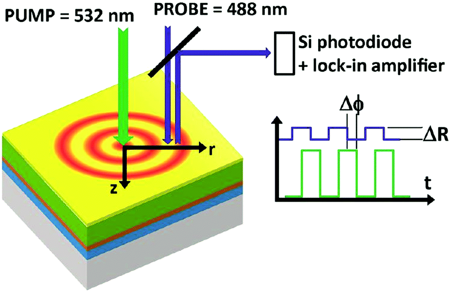 | ||
| Fig. 5 Principle of a modulated photoreflectance experimental setup. Reproduced from ref. 85, with the permission of AIP Publishing. | ||
A modulated pump beam (532 nm) is focused onto a sample's surface to provide a modulated local heat source in a metallic film deposited on top of the perovskite film. The heat diffuses laterally on the surface (r direction) and perpendicularly to the sample's surface (z direction). A periodic modulation of the surface reflection coefficient ΔR as a result of the periodically induced surface temperature modulation is sensed by a CW probe beam (488 nm) and a lock-in amplifier.
Theoretical thermal models86 are used which describe the magnitude (ΔR) and the phase (ΔΦ) of the modulated photoreflectance signal measured as a function of the distance to the pump beam. To get access to the thermal conductivity and diffusivity of the perovskite film in the r direction and the z direction (depending on the crystalline orientation of the film) the different layer systems underneath must be analysed beforehand. Moreover, photo-induced degradation,87 slight changes in the optical properties of MAPbI3 perovskite across the tetragonal to cubic transition,88 and possible degradation under intense optical excitation89 must be taken into account. For the sake of completeness, it should be mentioned that, besides these modulated heating techniques, thermal diffusivity measurements using a pulsed laser heating source for transient picosecond time-domain thermal-reflectance (TDTR) were presented.90 Although the results of the first TDTR measurements of MAPbI3 thin films62 significantly differ from other results (thermal conductivity of MAPbI3 films of 11.2 W (m K)−1 at RT), this method is promising because a theoretical description for frequency modulated time delay photo-thermal and photo-acoustic wave spectroscopies is given.91 Note that the optical generation of excess carriers due to laser excitation may significantly affect the thermal conductivity measurements. Thus, a possible explanation for the higher thermal conductivity determined by this technique might be linked to the contribution of the optically generated charge carriers to the thermal transport. The previously only theoretically predicted anisotropies in perovskites correlated with direction-dependent variations of the phonon vibrational density of states31 could be recorded by a differential photo-acoustic method to measure the thermal conductivity of thin films.92 Details of heat flow analysis in layered structures using a picosecond optical pump-and-probe technique can be found elsewhere.93
In addition to the space and time domains, thermal properties have been measured in the frequency domain. Nowadays, frequency-domain thermo-reflectance (FDTR) is used besides TDTR to simultaneously measure in-plane and cross-plane thermal properties.94 This technique can determine the thermal conductivity and heat capacity of a sample at the same time and it combines the advantages of TDTR with the relative experimental simplicity of modulated photo-thermal methods. Using FDTR, the thermal conductivities of various single crystal lead-halide perovskites were found to be proportional to ca-cubic·vs/3, where ca-cubic is the volumetric heat capacity of acoustic phonons based on a cubic unit cell and vs is the speed of sound.30 An average acoustic phonon mean-free path ![[capital Lambda, Greek, macron]](https://www.rsc.org/images/entities/i_char_e0bb.gif) a = 4.3 nm was determined. Thus, it could be shown that this technique is very promising for the determination of thermal properties.
a = 4.3 nm was determined. Thus, it could be shown that this technique is very promising for the determination of thermal properties.
Further advantages of these various techniques of thermal wave microscopy and their application for testing of micro- and nano-structured materials and devices are given in the review by Galovic et al.95 A review of other commonly used differential scanning calorimetry techniques is given by Gill et al.96 Note that, in addition to the drawbacks of the so far presented far-field thermal measurement methods, it is well known that thermal transport strongly depends on the dimensions of the materials and is of growing interest upon shrinking the film thickness.97–99 In this regard, innovative near-field thermal microscopy techniques open a non-destructive route to determine the thermal properties of perovskites beyond reach for classical thermal measurement techniques.
Good candidates are scanning probe microscopy based techniques with the opportunity to increase the spatial resolution of established analysis techniques on semiconducting perovskite materials and devices.100 The first atomic force microscopy based measurement technique for local thermal conductivity, called Scanning Thermal Microscopy (SThM), was invented in 1992.101 Shortly afterwards, the heat source and the temperature sensor were combined in one single element by means of resistive thermal probes for local heat transport analyses with high spatial resolution.102,103 This combined probe made SThM more and more important for a wide range of thermal property studies of crystalline solids, organic materials, and material compounds for (opto-)electronic applications because a range of thermal properties, such as heat transport, glass transition, melting, recrystallization, and thermal decomposition, can be obtained locally with high spatial resolution.104–109
The established macroscopic 3ω-technique110 by means of a modulated heating source was adapted to SThM for improved thermal transport measurements.111 The conventional 3ω technique, where the amplitude of the temperature oscillation of a line-shaped heat source mounted on a sample and powered using an AC thermal current (I0sin(ωt)) is measured logarithmically as a function of the angular frequency ω, has been used to determine the thermal conductivities of lead free perovskites.70–72 Meanwhile, the thermal conductivities of hybrid halide perovskite (MAPbX3; X = I, Br, and Cl) single crystals and thin films were first analysed by SThM without the need for extensive sample preparations.61 The thermal conductivity is determined from the slope of the measured amplitudes of the temperature oscillations ![[T with combining circumflex]](https://www.rsc.org/images/entities/i_char_0054_0302.gif) probe of the thermal probe vs. ln(ω). In order to map local thermal conductivities with high resolution, the resistive thermal probe of the SThM is powered by a mixed signal of angular frequencies ω1 and ω2 (see Fig. 6).50ω1 and ω2 are chosen to be the lower frequency limit ωmin and the upper frequency limit ωmax of the thermal probe. The resulting probe are detected in the frequency domain at 3ωmin and 3ωmax by lock-in amplification for signal to noise improvement by using the output signals of a Wheatstone bridge independently of the ambient probe temperature. The thermal conductivity can be obtained from the difference of these signals using calibrated material references and is particularly suited to assess the thermal transport in thin films, as the interaction volume is ultra-small.112,113 The local thermal diffusivity and thus indirectly the local volumetric heat capacity can be determined simultaneously because the local heat flux into the perovskite sample is given by this experiment. Hence, the thermal transport properties of CsPbCl3 thin films across phase transitions have been analyzed by controlling the sample temperature.51 Since SThM is an AFM based microscopy technique, the thermal expansion coefficient can be measured simultaneously within the same range of temperatures in addition,61 expanding the capability of this instrument. Large negative and positive linear thermal expansion coefficients were found for the tetragonal and pseudo-cubic phases of MAPbI3 single crystals respectively.33,61 Since the resulting thermal stress and structural instability lead to the degradation of perovskites,114 the determination of the thermo-elastic quantities of perovskites depending on the temperature is focused on in the following.
probe of the thermal probe vs. ln(ω). In order to map local thermal conductivities with high resolution, the resistive thermal probe of the SThM is powered by a mixed signal of angular frequencies ω1 and ω2 (see Fig. 6).50ω1 and ω2 are chosen to be the lower frequency limit ωmin and the upper frequency limit ωmax of the thermal probe. The resulting probe are detected in the frequency domain at 3ωmin and 3ωmax by lock-in amplification for signal to noise improvement by using the output signals of a Wheatstone bridge independently of the ambient probe temperature. The thermal conductivity can be obtained from the difference of these signals using calibrated material references and is particularly suited to assess the thermal transport in thin films, as the interaction volume is ultra-small.112,113 The local thermal diffusivity and thus indirectly the local volumetric heat capacity can be determined simultaneously because the local heat flux into the perovskite sample is given by this experiment. Hence, the thermal transport properties of CsPbCl3 thin films across phase transitions have been analyzed by controlling the sample temperature.51 Since SThM is an AFM based microscopy technique, the thermal expansion coefficient can be measured simultaneously within the same range of temperatures in addition,61 expanding the capability of this instrument. Large negative and positive linear thermal expansion coefficients were found for the tetragonal and pseudo-cubic phases of MAPbI3 single crystals respectively.33,61 Since the resulting thermal stress and structural instability lead to the degradation of perovskites,114 the determination of the thermo-elastic quantities of perovskites depending on the temperature is focused on in the following.
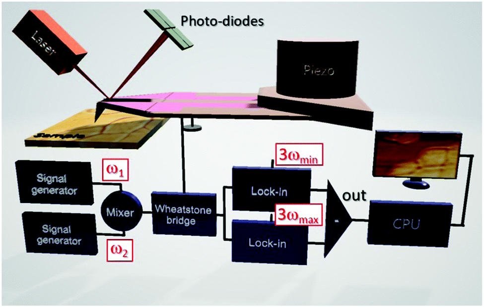 | ||
| Fig. 6 Schematic illustration of extended quantitative thermal conductivity measurements by SThM applying the so-called 3ω-technique in the frequency domain. Reprinted with permission from ref. 50. Copyright (2019) American Chemical Society. | ||
Thermo-elastic quantities of perovskites
In particular, heat induced degradation (e.g., decomposition) under extreme operating conditions, for example under intense solar light irradiation, must be considered.The melting temperature of CsPbI3 was determined in 1992 from the phase diagram obtained by differential thermal analysis (DTA) experiments to be higher than 480 °C at atmospheric pressure.115 A short time later, subsequent studies of crystal structures exhibited that CsPbBr3 melts at 567 °C and crystallizes from the melt at 514 °C.116 At the same time it could be demonstrated that melting points increase with decreasing atomic number, i.e. for CsPbCl3 up to 615 °C.117 All these compounds melt congruently as confirmed in these experiments. Hence, large CsPbBr3 crystals could be produced from the melt at high temperatures (600 °C) using the vertical Bridgman method.116 These single crystals have been proposed as promising candidates for X-ray and gamma-ray detection,118–120 since the first investigations on these direct semiconductors showed that most of their properties are comparable to, or even exceed, those of commercial state-of-the-art detector materials.
In this context it must be taken into account that the endothermic DTA peaks for the decomposition pathways of MAPbX3 compounds are reported to be low.121 However, although various decomposition reactions have been proposed:121–124
| MAPbX3 → PbX2 + MA + HX | (3) |
| MAPbX3 → PbX2 + MAX | (4) |
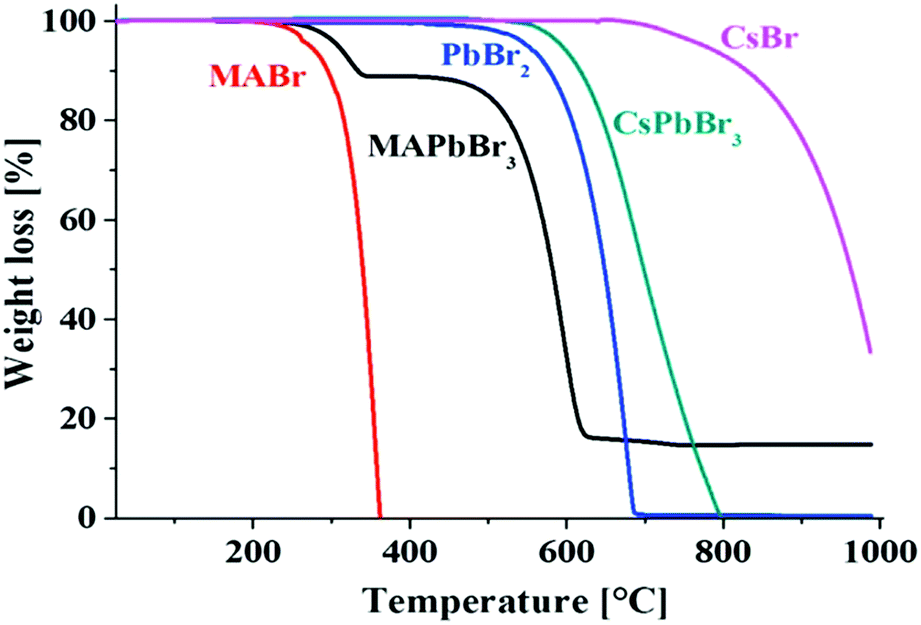 | ||
| Fig. 7 Thermogravimetric analyses of MABr, MAPbBr3, PbBr2, CsPbBr3, and CsBr, showing the higher thermal stability of the inorganic perovskites compared to the hybrid organic−inorganic perovskites. Reprinted with permission from ref. 125. Copyright (2016) American Chemical Society. | ||
With respect to the evaporation or decomposition of CsPbBr3, CsBr is more stable than PbBr2, which is lost first. The small temperature shift between PbBr2 and CsPbBr3 can be explained by the slightly higher stability of the perovskite compound. For hybrid perovskites, it must be considered that all the methylammonium halides have lower melting points (for instance MAI: >190 °C123). Although they are mostly even reported to be over 200 °C121 for MAPbX3, it is still a challenge to have long-term stabilities at 85 °C (representing an elevated temperature on a roof on a hot summer day) required according to the International Standards (IEC 61646 climatic chamber tests) of solar cells.16 Thus the thermal activation energies (Ea) for the decomposition reactions have to be considered.126 From DTAs Eas of 68 ± 2 kJ mol−1, 60 ± 10 kJ mol−1, and 80 ± 20 kJ mol−1 have been reported for MAPbCl3, MAPbBr3, and MAPbI3, respectively.121 Somewhat larger Ea values have been determined by the first mass loss step observed in thermogravimetric analyses.127 Even much higher values have been found for lighter halides in MA and FA based compound calculations,128 summarized in Table 3.
| Perovskite | E a [kJ mol−1] | α [×10−4 K−1] |
|---|---|---|
| MAPbI3 | 93 ± 8127 | α tet.(001): −5.1, αcub.(001): 4.661 |
| 83128 | α tet.(001): −1.06, αtet.(100): 1.32 | |
| α cub.(100): 0.4833 | ||
| α tet.(100): 0.58, αcub.(100): 0.3963 | ||
| α tet.: 0.90135 | ||
| MAPbBr3 | 98 ± 4127 | α cub.(100): 0.33136 |
| 365128 | α cub.(100): 0.3263 | |
| α cub.: 0.67135 | ||
| MAPbCl3 | 400128 | α cub.(100): 0.2963 |
| CsPbI3 | 650 ± 90127 | α ort.: 0.39, αcub.: 0.39137 |
| α ort.(001): 0.22 | ||
| α ort.(110): 0.22 | ||
| α tet.(001): −0.52 | ||
| α cub.(100): 0.40138 | ||
| CsPbBr3 | α ort.: 0.38, αtet.: 0.65, αcub.: 0.26139 | |
| α ort.(101): 0.38140,141 | ||
| CsPbCl3 | α mon.: 0.56, αort.: 0.50, αtet.: 1.27 | |
| α cub.: 0.3014 | ||
| α cub.: 0.22@T = 85 °C142 | ||
| α mon.: 0.42, αort.: 0.38, αtet.: 0.78 | ||
| α cub.: 0.29139 | ||
| FAPbI3 | 115 ± 3127 | α tet.(100): 0.77 |
| 108128 | α tet.(010): 0.77 | |
| α tet.(001): 0.49143 | ||
| α ort.: 0.39135 | ||
| FAPbBr3 | 133 ± 1127 | α cub.: 0.89135 |
| 332128 | ||
Note that these values do not reflect possible reliability issues related to other causes of degradation.129–131 Details of the chemical, structural, morphological, and optical stability and the impact of thermal stress on the charge transport layers of methylammonium lead halide based perovskites are available elsewhere.114 The main difference between the stability of hybrid and all-inorganic perovskite halides was found to be due to the different chemical properties of the A-site cations, because their entropic contribution to free Gibbs energy is of utmost importance to understand the intrinsic stability of these compounds.132 While a number of stability issues may be solved with proper encapsulation,133 it has to be noted that a critical intrinsic stability problem arises from the behavior under thermal mechanical stress. To make matters worse, it has long been known that perovskites have phase transitions at elevated temperatures up to 85 °C.13,134
Phonon coupling mechanisms in perovskites
The first investigations of the elastic constants and thermal expansion of CsPbCl3 were provided by Hirotsu and Suzuki in 1978.14 They evidenced the phase transitions for CsPbCl3 single crystals from monoclinic to orthorhombic to tetragonal and finally to cubic, as claimed earlier.44,45 A notable expansion (Δl/l) of 16.7 × 10⁻⁴ as detected using a conventional dilatometer is correlated with first order transitions from tetragonal to cubic phases. No signs of discontinuity of Δl/l(T) were found at the other phase transitions that would indicate a first order transition.14 Therefore, these transitions would be second order which is in contradiction to an earlier report which claimed the transition from monoclinic to orthorhombic to be of first order.44,45 Another point noted was that Δl/l in the cubic phase is nearly linear with temperature. One year later, some nonlinearities were found for the lattice thermal expansion up to 85 °C of CsPbCl3, with α(T)CsPbCl3 being quadratically dependent on T in the cubic phase.142 However, although Δl/l was determined to be less than 3.1 × 10⁻⁴ from the tetragonal to cubic phases of CsPbCl3, a much higher value of 5.8 × 10⁻⁴ was found in the case of CsPbBr3.139 In this paper the thermal expansion coefficients of CsPbCl3 were determined to be lower than those reported earlier, as can be seen from Table 3.The volume thermal expansion coefficients have been studied for CsPbI3 from the temperature dependency of the unit cell volume as (1/V0)·(dV/dT), where (dV/dT) is the change in the volume in the corresponding temperature interval and V0 is the volume at the reference temperature T0.137 The same volume thermal expansion coefficient of 1.18 × 10⁻⁴ K−1 has been determined for orthorhombic CsPbI3 (γ-phase) and cubic CsPbI3 (α-phase), with a large discontinuous volume change of about 6.9% at this transition. Assuming CsPbI3 to be isotropic in the first approximation, the volumetric expansion coefficient is three times the linear coefficient and would thus be slightly larger than those of CsPbBr3 and CsPbCl3. Note that it is still a challenge to stabilize the tetragonal phase (β-phase) of CsPbI3 perovskite at ambient temperature. Despite theoretical calculations predicting the β-phase to be more stable than the α-phase,144 experimentally the β-phase is difficult to obtain and to stabilize;145 thus thermal expansion measurements on β-CsPbI3 are extremely rare, to our knowledge.138,146
Large negative thermal expansion coefficients have been observed in the tetragonal phase for yellow and black CsPbI3 (see Fig. 8). This complicates the application in optoelectronic devices because only the CsPbI3 perovskite black phase is optically active. Due to their huge absolute values of thermal expansion coefficients, perovskite films fabricated by existing methods are strained, and the strain is caused by the different coefficients of thermal expansion of the perovskite and substrate during thermal annealing processes as well as due to the growth process itself. It should be noted that films have either compressive or tensile strains in the in-plane direction, which lead to tensile or compressive out-of-plane strains, respectively. Strain has been shown to accelerate the degradation of perovskite films under illumination, which can be explained by increased ion-migration in these films.147
 | ||
| Fig. 8 Structural phase kinetics of strained α-, β-, and γ-CsPbI3 perovskite thin films. From ref. 138. Reprinted with permission from AAAS. | ||
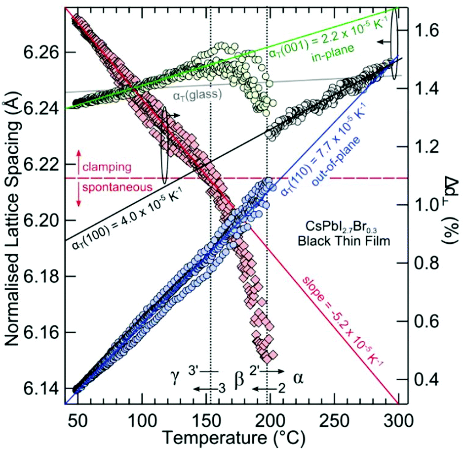
The strain might significantly influence the determination of thermal expansion coefficients. For example, although negative thermal expansion coefficients have been detected in the tetragonal phase for MAPbI3 perovskites, a five times larger value of αc-tet. = −5.1 × 10⁻⁴ K−1 has been found for single crystals61 compared to αc-tet. = −1.06 × 10⁻⁴ K−1 determined for thin films.33 Moreover, the thermal expansion coefficients in the cubic phase of MAPbI3 have been reported to be one order larger than those in single crystals. In this context, it must be noted that no discontinuity in thermal expansion has been detected at the phase transition of single crystals in the c-direction. Furthermore, it must be considered that the thermal expansion coefficients depend on the direction in the crystal. αa-tet. is reported to be positive and 1.32 × 10⁻⁴ K−1 for these thin films.33 The thermal expansion coefficients determined for the different crystal orientations are summarized in Table 2 in addition.
Note that negative thermal expansion coefficients are generally associated with materials that exhibit ferroelectric, ferromagnetic, or charge-transfer phase transitions that cause the material to contract on increasing the temperature due to either a redistribution or an ordering of ferroelectric/-magnetic domains.148 When discussing the ferroelectricity of perovskites, it must also be considered that as the film thickness decreases, stable domain patterns can change from a ferroelectric–ferroelastic domain to a ferroelectric one, which alters the domain size.149 A challenge for the detection of ferroelectric domains, for instance demonstrated by piezo-response force microscopy on MAPbI3 thin films,150 is that the domain size in thin films can be very small due to their rapidly decreasing thickness-dependence.
However, for the sake of completeness, it should also be mentioned that in comparison to films lower thermal expansion coefficients were determined for single crystalline MAPbI3 in the (100)-direction, αa-tet = 0.58 × 10⁻⁴ K−1 and αa-cub. = 0.39 × 10⁻⁴ K−1.63 A first order transition with a Δl/l of 2.64 × 10⁻⁴ was found in these directional studies. Nevertheless, it could also be demonstrated that the coefficient of thermal expansion of MAPbI3 is larger than those of MAPbBr3 and MAPbCl3 (0.32 × 10⁻⁴ K−1 and 0.29 × 10⁻⁴ K−1, respectively). In addition, the coefficients of thermal expansion of these hybrid perovskites are larger than those of related Cs–Pb-based all-inorganic perovskites. A larger thermal expansion coefficient was even detected for the lead-free double perovskite (MA)2AgBiBr6 compared to Cs2AgBiBr6 in their cubic phase (0.44 × 10⁻⁴ K−1 and 0.28 × 10⁻⁴ K−1 in the (111)-direction respectively).151,152 The higher thermal expansion coefficient was attributed to the weaker chemical bonds associated with the softer perovskite (MA)2AgBiBr6.63
Finally, it must be pointed out that for the black phase of γ-CsSnI3, the coefficient of the volumetric thermal expansion at RT was measured to be quite large (1.26 × 10⁻⁴ K−1).153 The coefficients of the linear thermal expansion were determined to be αa-ort.: 0.50 × 10⁻⁴ K−1, αb-ort.: 0.14 × 10⁻⁴ K−1, and αc-ort.: 7.71 × 10⁻⁴ K−1. The coefficient of volumetric thermal expansion in β-FAPbI3 (2.06 × 10⁻⁴ K−1) was reported to be two times larger than that in the α-phase.143 This ultra-large volumetric thermal expansion creates substantial challenges in device applications. Note that the volumetric thermal expansion is significantly reduced in the cubic α-phase, which corresponds to a negative contribution for large amplitude dynamic PbI6 octahedral tilts. In the α-phase, the linear thermal expansions are 0.77 × 10⁻⁴ K−1 in the ab-plane and 0.49 × 10⁻⁴ K−1 in the c-direction, suggesting again strong anisotropic mechanical properties. Two wide regions of large negative thermal expansion were found at low temperatures (−100 °C and −219 °C) for δ-FAPbI3.135 The linear thermal expansion for FAPbBr3 was determined to be 0.89 × 10⁻⁴ K−1 in the cubic phase at RT from these studies. The symmetry changes are linked again to the tilting of the octahedral (PbBr6) identified by complementary XRD analysis.
Besides that, the Young's modulus E and hardness H values of lead halide perovskite crystals are reported to be low.152,154 Thus, perovskite compounds can be considered as “soft materials”. The elastic moduli of single crystals vary in the range 10–20 GPa and a general trend of ECl > EBr> EI is observed at room temperature. The perovskite compounds can also be regarded as non-brittle, since H varies in the range 0.5–0.25 GPa with the trend HCl< HBr< HI. Metal-halide perovskite films can therefore facilitate applications in flexible devices that require plastic deformation. In this context, however, it should be kept in mind that their E and H strongly depend on the crystalline orientation. The implications of the thermo-mechanical behavior of metal-halide perovskites and interfaces in the reliability of solar cells, as well as opportunities for future research directions in this general area, are highlighted elsewhere.155
The first in-depth analysis of charge-carrier–phonon interactions in hybrid lead halide perovskites was carried out on FAPbI3, FAPbBr3, MAPbI3, and MAPbBr3.156 For FA-based perovskites it was already found that the Fröhlich interaction between charge carriers and LO phonons is the dominant contribution to the predominantly homogeneous broadening of the PL line width in these hybrid perovskites at room temperature (see Fig. 9). The Fröhlich interaction for bromide perovskites is larger than that for iodide perovskites, providing a link between composition and electron–phonon scattering that fundamentally limits the mobilities of the charge carriers. In addition to these spectral changes, the lattice strain causes non-radiative losses in halide perovskites,157 which has in addition been attributed to the locally induced crystal misorientation.158 The remaining nanoscale strain also reduces the stability in cesium-lead-bromide perovskites and shifts the local luminescence spectrum.159 In contradiction to these studies, it has been reported previously that light-induced lattice expansion leads to high-efficiency perovskite solar cells.160 While the authors of these studies claim to exclude heat-induced lattice expansion, it has been shown that the lattice expansion mechanism matches the heat-induced thermal expansion during illumination.161
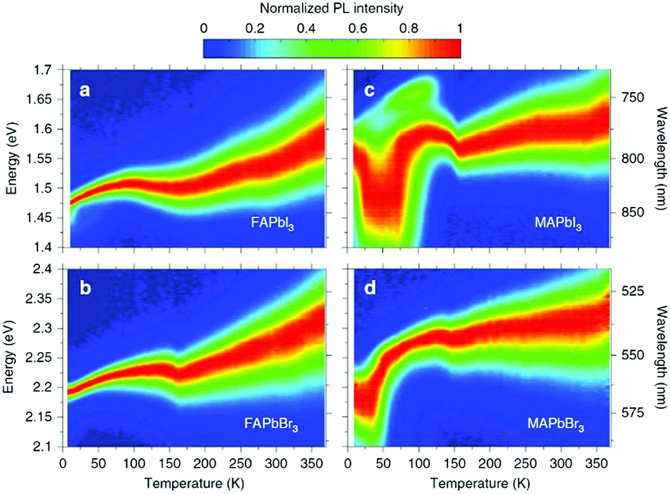 | ||
| Fig. 9 Temperature dependence of normalized steady-state PL on (a) FAPbI3, (b) FAPbBr3, (c) MAPbI3, and (d) MAPbBr3. From ref. 156. Reprinted with permission from Springer Nature. | ||
In summary, the information provided so far can be used to predict changes in the optical and charge transport properties of devices, since any structural change has a serious impact on the phononic and electronic structures.162 The properties of phonons are crucial for the understanding of not only charge transport in the form of electron–phonon interactions in polar semiconductors such as halide perovskites, but also for heat transport in functional materials. Phonon–phonon scattering plays a decisive role in determining acoustic phonon transport and thus the thermal conductivity of halide perovskites. Details about these coupling mechanisms have recently been summarized in the review article of Haque et al.25 In addition, in terms of the soft nature of halide perovskites, temperature and pressure are expected to have a strong influence on the crystal growth and the boundary fusion of these materials.
Thermo-mechanical patterning
Metal-halide perovskites are easily damaged by various solvents. Thus, conventional photolithography processes are usually not an option to pattern halide perovskites.163 Therefore, creating nanoscale perovskite optoelectronic devices by well-controllable, low-cost fabrication methods while simultaneously maintaining high optoelectronic performance is a challenge.164Wang et al. were able to show first that, similar to other “soft materials”, MAPbI3 can directly be patterned by thermal nanoimprint lithography (NIL) at low temperatures (100 °C), since electrostatic interactions dominate in ionic MAPbI3 crystals (see Fig. 10a).165 In these studies, nanoimprinted photodetectors were demonstrated with significantly improved performance compared to nanoimprinted devices. The performance enhancement was attributed to the NIL-induced improved crystallinity; particularly, the nanograting structure was favorable for better photon absorption and charge carrier transport. NIL has also been employed for the fabrication of meta-surfaces.166,167 By using a flat stamp in NIL, it could be shown that this imprinting process is able to substantially flatten an initially very rough polycrystalline hybrid perovskite layer and to transform it to a thin film consisting of laterally extended crystals on the order of tens of microns with a surface roughness below 1 nm (rms) (see Fig. 10b).61,168,169 A notable effect of this planar hot-pressing procedure was that these grains have similar physical properties to single crystals, e.g., the same thermal conductivity and PL-lifetime. Besides that, the films are well oriented and show enhanced stability when exposed to ambient air.169 The latter evidences earlier observations of enhanced stability of larger crystal grains.171 Recently, the planar NIL fabrication of continuous MAPbI3 quasi-single-crystal films composed of even 100 μm large-sized grains with deep boundary fusion has been reported.172 Here, a remarkable decrease of trap density (ntrap: 7.43 × 1011 cm−3) determines a long carrier lifetime (τ: 1.7 μs). Thus, planar hot-pressing has a lot of advantages in comparison to other procedures to produce large crystals.173–175 The ability to form nanostructures is particularly important for the preparation of resonator structures for metal-halide perovskite lasers.176 Hence, photonic nanostructures were patterned by thermal NIL directly into MAPbI3 perovskite films using nanopillar molds (illustrated in Fig. 10c).170 Apparently, surface defects which cause substantial recombination and luminescence quenching were eliminated by recrystallization upon thermal imprinting. The resulting 2D photonic crystal (2D-PC) lasers showed low lasing thresholds of 3.8 μJ cm−2. The first distributed feedback (DFB) lasers based on MAPbBr3 thin films with a linear second order photonic grating (periodicity: 300 nm) directly imprinted into the active layers were also presented.169 Very low lasing thresholds of 3.4 μJ cm−2 were achieved in these optically pumped DFB laser structures. Using a flat stamp to recrystallize the layer via NIL, it was shown that a significantly lowered threshold for the onset of amplified spontaneous emission (ASE) compared to pristine films was achieved due to reduced optical scattering. Note that low lasing threshold levels are essential on the way to the first electrically operated perovskite laser diode. A scalable lithographic scheme for thin organic metal-halide perovskite films has already been demonstrated and utilized for the realization of perovskite micro lasers.177
 | ||
| Fig. 10 (a) Schematic of a NIL process with a Si flat, nanopillar, and nanograting mold. Reprinted with permission from ref. 165. Copyright (2016) American Chemical Society. AFM images of (b) pristine and (c) planar hot-pressed MAPbBr3 layers. From ref. 169. Copyright Wiley-VCH Verlag GmbH & Co. KGaA. Reproduced with permission. (d) SEM image of the 2D-PC with dimensions of the triangular grating. Inset (bottom): Photograph of the sample under oblique while-light illumination. Inset (top): First Brillouin zone of the 2D-PC with labelled points of high symmetry. (e) Emission spectra upon optical pumping with increasing energy density (1.6–4.7 μJ cm−2). A scaled PL spectrum of a pristine MAPbI3 layer upon cw-excitation is shown for comparison. From ref. 170. Copyright Wiley-VCH Verlag GmbH & Co. KGaA. Reproduced with permission. | ||
It is noteworthy that all-inorganic metal halide perovskite films based on Cs can likewise be structured and flattened using NIL at temperatures <150 °C.50,51,178 The first CsPbBr3 thin-film DFB and vertical cavity surface emitting lasers (VCSELs) with an ultralow threshold (2.2 μJ cm−2, 300 ps pump pulses) operating at room temperature, which do not rely on the use of nanoparticles, were thus realized by NIL.178 In addition, the planar hot-pressing procedure enabled the creation of 0D, 2D, and 3D perovskite films depending on the stoichiometry of the pristine layer.50,51
In conclusion, these results indicate that NIL will be an excellent thermo-mechanically supported process platform for the patterning of metal-halide perovskites in the future.51 Thermal NIL can improve the crystal quality as well as create the required patterns. However, although there are initial approaches to describe the crystal quality improvement and the growth processes by NIL, a detailed simulation model of this hot-pressing method for perovskites has not been developed yet.
In addition, it must be noted that a strong temperature-dependence of stimulated emission has been observed in MAPbI3 thin films.179 A heating of up to ≈50 °C has been detected at RT in the first few hundred ns following pump turn-on, which leads to a dynamic increase in threshold and limits continuous-wave lasing in hybrid perovskite semiconductors. Furthermore, Joule heating prevents hybrid LEDs from reaching current densities greater than a few hundred A cm−2 without total emission quenching.180 Therefore, an improvement in heat dissipation and a reduction in the pulse width are inevitable for proper operation. The first effective thermal management strategies were proposed by L. Zhao et al., which enables bright and stable perovskite LEDs.181
Strategies to enhance the thermal properties of transport layers in perovskite devices
Niu et al. reviewed the stability of metal-halide perovskites in environments such as oxygen and moisture, upon UV illumination, and under thermal stress.182 They discussed the impact of processing conditions and noted that, to stabilize perovskites, many factors must be considered in device design, e.g., the composition and crystal structure of the perovskites, choice of electrode materials and charge transport layers, processing technology and encapsulation concepts.Concepts for enhancing grain sizes, improving crystallinity, changing elastic properties and passivation of perovskite films by using organic additives were introduced.183,184 In these studies, the inclusion of various additives in MAPbI3 was examined and a significant improvement in mechanical robustness was observed. Besides, a dimensionality-controlled surface passivation for enhancing the performance and stability of perovskite solar cells has been pointed out recently.185 Note that in metal-halide perovskites the thermal properties of 0D and 2D materials significantly differ from those of the bulk (3D) and are thus discussed in the following section.
In order to combine charge transport and chemical protection in one, great efforts have also been made to produce functional layers with optimized optical, electrical and permeation barrier properties.186 Brinkmann et al. demonstrated that introducing a bi-layered electron-extraction interlayer consisting of aluminium-doped zinc oxide nano-particles and tin oxide, grown by low temperature atomic layer deposition (ALD), can significantly mitigate the decomposition of the perovskite in inverted perovskite solar cells even at elevated temperatures.187,188 It should be noted that in this example the ALD-grown tin oxide formed an outstandingly dense permeation barrier.
The reduction of stress and strain in films is also an important issue that should be addressed for the reliability of perovskite devices. Unfortunately, only a few studies have been carried out so far. Rolston et al. studied mechanical stresses that develop during the fabrication of perovskite films and a direct relationship between film stress and stability in both perovskite films and solar cells was determined.189 They developed simple strategies to reduce the stress and to improve the inherent moisture and thermal stability of perovskite films, e.g., by using low process temperatures, using polymeric substrates with thermal expansion coefficients that are closer to those of the perovskites, and pre-straining the substrate during perovskite processing. Otherwise highly textured morphologies are created by popular anti-solvent conversion methods due to in-plane compressive stress.190 The energy release leads to wrinkling during the intermediate phase of film formation, in which the substrate constrains the film from expanding. Ultra-smooth films can be obtained by slowing the rate of film formation since the extent of wrinkling is correlated with the rate of film conversion.
The regulation of strain in perovskite thin films by suitable selection of charge transport layers (CTLs) was also reported (the energy level alignment is shown in Fig. 11).191 Tensile strains in perovskite films were compensated for by transport layers with high thermal expansion coefficients and by elevating the processing temperature.
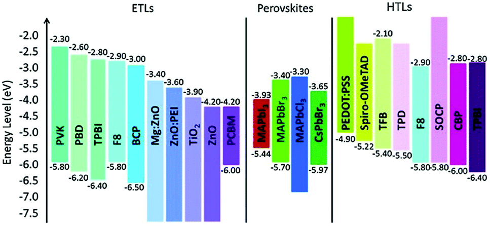 | ||
| Fig. 11 Energy level alignment of various materials used as ETLs and HTLs in perovskite devices. From ref. 192. Reprinted with permission from Elsevier. | ||
Note that thermal effects can also impact other functional layers in perovskite devices, such as CTLs and electrodes. The extensive studies on their thermally enhanced chemical decompositions and strategies for their stabilization are reviewed in the article by Ava et al.114 For example, metal electrodes, which might contribute to thermal management, can be degraded by the corrosive decomposition products of the perovskite. These layers must therefore also be protected. This is even more problematic for semi-transparent solar cells, in which the semi-transparent electrodes are based on ultrathin metal films. Thus, a self-encapsulating thermostable and air-resilient electrically conductive permeation barrier was realized by an ultrathin Ag layer sandwiched between SnOx grown by low-temperature atomic layer deposition.193 These additional layers further complicate the design of components in terms of mechanical stability. The efforts to increase the energy of fracture of perovskite solar cells were compiled by Boyd et al.194
Although recent review articles discuss factors affecting the chemical and mechanical stability of perovskite solar cells as well as current issues and new strategies to push material and device stability,195,196 strategies for improved heat management in perovskite devices have not yet been engineered. It must be ensured that the other important layers within the devices can dissipate the heat because perovskites have a very low thermal conductivity. For example, in addition to a low coefficient of thermal expansion of 5 × 10⁻⁶ K−1, glass has a very low thermal conductivity of approximately 1 W (m K)−1 and a very low specific heat capacity in the range of 0.8 J (g K)−1, which prevents heat dissipation into this substrate.197 The commonly used transparent electrode material indium tin oxide (ITO) is degenerately doped (carrier density >1 × 1020 cm−3) and behaves like a metal.198 Nevertheless, the resulting in-plane heat transport in the ITO layer is strongly limited by its low λITO = 6 W (m K)−1 and a typically small film thickness of around 150 nm. In addition, it must also be noted that organic-based ETLs and HTLs, which are depicted in Fig. 11, have likewise ultra-low thermal conductivities (λPCBM = 0.031 W (m K)−1), and are highly anisotropic for the in-plane and out-of-plane directions (λPEDOT:PSS‖ = 1 W (m K)−1 and λPEDOT:PSS⊥ = 0.3 W (m K)−1, respectively).199–201 Thus, instead of organic-based charge transport layers, metal-oxide-based compounds, which have significantly higher thermal conductivities, could be used for improved thermal management. Polycrystalline Al-doped ZnO films, for instance, have more than one order higher thermal conductivities in the range of λZnO = 6 W (m K)−1 at RT and are therefore ideal for additional heat dissipation in ETLs.202 The same applies to TiO2 layers with λTiO2‖ = 12.6 W (m K)−1 and λTiO2⊥ = 8.8 W (m K)−1.203 Metal-oxides have also evolved as a powerful class of materials on the anode side.204 Transition metal oxides like MoO3, WO3, and V2O5 have successfully been introduced in organic and perovskite solar cells, which should enable enhanced thermal transports in HTLs.205 Charge transport layers based on graphene or silver nanowires are further potential candidates in heat management and have also been studied in recent years.206,207 Note that, in general, many strategies that have been proposed for the thermal management in organic devices can be used in the field of perovskites.68
In addition to the absolute values of thermal conductivities for the respective materials, it has to be considered that heat transport in the perovskites is due to phonons, while in the electrodes it is mostly associated with electrons. Therefore, it must be ensured that the heat transport at this interface is not limited by its thermal impedance. In order to guarantee an optimized heat flux, an enhancement of the thermal boundary conductance of such a system has recently been demonstrated by nm sized additional adhesion layers, either titanium or nickel.208 In this context it should likewise be mentioned that very thin layers can be considered as thermally transparent depending on their mean-free phonon and electron path lengths.112,113 This means that additional thin functional layers that do not impair the heat flow can be used in the design of metal-halide devices.
Although the effectiveness of heat spreading concepts is often directly related to the thermal conductivity of the materials used, alternative passive means of cooling should be considered, as well.209 One is to use CTLs with an elevated specific heat, which can absorb the heat generated during dynamic device operation. A different procedure is to effectively store heat dissipated from the electronic components, which is periodic in nature or suddenly temporary, using high latent heat materials (see the Thermal properties across phase transitions section). The use of materials with solid and liquid organic phase changes has previously been proposed with regard to the thermal management of mobile phones210 and the practical applications of liquid-phase-exfoliated graphene as filler material in phase change materials have been outlined.211 A review of the thermal properties of graphene, few-layer graphene and graphene nanoribbons has also been provided therein along with a discussion of practical applications of graphene in thermal management and energy storage.
Dimensionalities of metal-halide perovskites
As predicted in the recent review article by Cao et al., low-dimensional-networked metal-halide perovskites may be useful for a wide range of applications.78 The incorporation of these compounds has been shown to improve the optical properties and stability of devices, such as all-inorganic 0D/3D mixed-dimensional perovskite solar cells.212,213 Overall, low-dimensional perovskites and their composites have been employed in a wide variety of applications, such as LEDs, solar cells, lasers, photodetectors and stimuli-responsive devices. Although the thermal properties of these 0D and 2D perovskite materials can differ significantly from those of the corresponding 3D analogues, as of yet, only a few studies have been carried out to assess heat transport in low-dimensional perovskites.32,50,51,214,215An ultralow thermal conductivity of 0.15 W (m K)−1 was discovered in 0D hybrid lead-free [Mn(C2H6OS)6]I4 single crystals at room temperature; it was further decreased by introducing disorder into the system.214 Furthermore, the thermal conductivities of 2D hybrid perovskites could be varied in a range from 0.10 to 0.19 W (m K)−1 depending on the molecular substructure of ammonium cations (details of the thermal properties can be obtained from Table 1).32 The extremely low thermal conductivities can be attributed to the crystalline substructures of these perovskites. In a similar sense, substantially reduced thermal conductivities have been discussed for layered, 2D complex thermoelectric materials.216 This effect has been explained by increasingly glass-like properties, which hamper phonon propagation. Moreover, the low thermal conductivity found in 0D perovskites has earlier been associated with their soft phonon dispersion.77 It was found that the thermal conductivities of these perovskite films, due to the anisotropy of the crystalline structure, are significantly dictated by their relative orientation (see Fig. 12). The results presented so far suggest that organic based low-dimensional perovskites provide a unique opportunity to achieve ultralow thermal conductivity, which would be beneficial for thermo-electric applications.
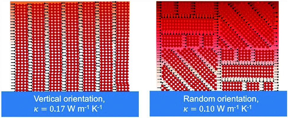 | ||
| Fig. 12 Schematic illustrations of vertically and randomly oriented BA2MA3Pb4I13 crystal orientations that lead to different thermal conductivities. Reprinted with permission from ref. 32. Copyright (2020) American Chemical Society. | ||
For all-inorganic perovskites, such as caesium lead chloride, it could be demonstrated for 3D phase CsPbCl3, 2D phase CsPb2Cl5, and 0D phase Cs4PbCl6 that the thermal conductivities as well as volumetric heat capacities become smaller upon reducing the dimensionality (see Table 4).51,215 Note that the thermal diffusivities, which are responsible for the dynamic heat transfer in devices, remain almost constant within the measurement uncertainties. Thus, the presented results offer a promising general route for designing 0D and 2D materials for future materials with exceptional thermal properties.
In another example, 2D phase CsPb2Br5 films show a low thermal conductivity of 0.33 W (m K)−1, a low thermal diffusivity of 0.3 mm2 s−1, and a small heat capacity of 0.18 J (g K)−1, which are drastically lower than those of their 3D counterparts (shown in Table 1).50
Thermal properties across phase transitions
Even though phase transitions have a significant impact on various physical properties, only a few studies have been carried out to assess the thermal properties of metal-halide perovskite in the vicinity of phase transitions.51 This information is of particular interest if devices are operated in the respective temperature regime. Fig. 13 provides an overview of the crystal phase vs. temperature for some selected hybrid and all-inorganic perovskite representatives. In addition to variations of the dielectric constant and the band structure, which consequently alter the band gap, the optical absorption properties, the carrier dynamics (charge carrier mobilities), etc., discontinuities in the thermo-mechanical properties were reported, as discussed above. Besides, changes in thermal conductivity and heat capacity at first and second transitions are of particular interest, since they significantly influence the heat diffusivity and thus the heat management of perovskite devices.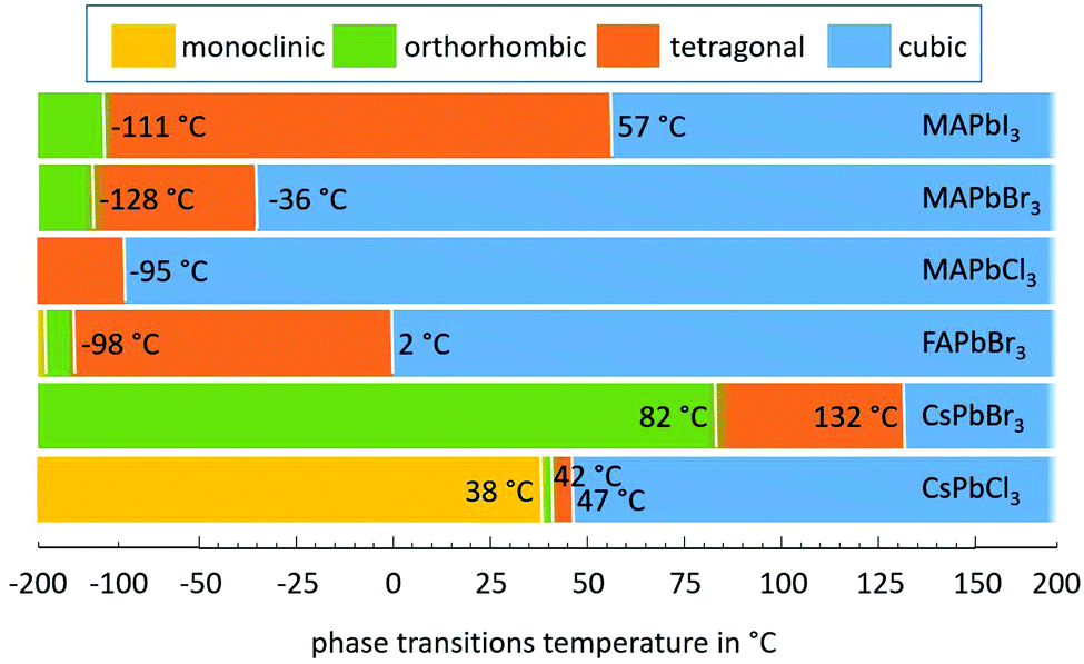 | ||
| Fig. 13 Schematic representation of the phase transitions of hybrid and all-inorganic perovskites.44–47,135,218 | ||
Briefly summarized, first and second order transitions from a monoclinic to an orthorhombic to a tetragonal structure at 37 °C and 42 °C, respectively, and a first order transition to a cubic structure at 47 °C have been reported for CsPbCl3 single crystals.44,45 The measurement showed that CsPbCl3 is neither ferroelectric nor antiferroelectric in any of the phases.44,46 The phase transitions are basically associated with the condensation of rotational modes of PbCl6 octahedra around the three principal axes.47 A considerable acoustic attenuation was observed in these experiments in the orthorhombic phase. The specific heat csp and thermal diffusivity a values of the different phases as well at their transitions were obtained in transient measurements on single crystals.11 Similarly, two characteristic phase transitions have been found for CsPbBr3, the orthorhombic/tetragonal at 82 °C and the tetragonal/cubic at 132 °C for temperatures above RT.217 Significant differences were reported out of these macroscopic investigations for the heat transitions obtained between powder samples and bulk samples, which was assumed to be due to many defects in the powder particles. Furthermore, the pulse transient method used in these studies did not evidence the expected behavior of csp(T) when going from the monoclinic to the orthorhombic to the tetragonal phase of CsPbCl3.11 Specifically, at a first order transition, one would expect a divergence of csp(T) due to the latent heat involved. Note that it is surprising that all these transitions occur within a temperature range of ΔT ≈ 10 °C in the case of CsPbCl3 measurement. More exceptionally, for CsPbBr3 the two phase transitions (orthorhombic–tetragonal–cubic) are separated by a ΔT = 50 °C.217 However, even though clear changes in csp(T) could be observed, this behavior did not agree with theoretical predictions of an abrupt change in csp(T).
The variation of the thermal properties across the phase transitions in the range from RT to 65 °C was recently analyzed for CsPbCl3 thin films by SThM. A significant increase of the thermal conductivity was found for the cubic phase (T > 46 °C), while only slight variations in λ() were detectable for transitions from the monoclinic to the orthorhombic to the tetragonal phase. It was demonstrated that upon transition to the cubic phase, the relative increase of average cvol.() is significantly higher than that of λ(), because a() and cvol.() measurements are extremely sensitive to the amount of heat ΔQ() involved in the respective transition. Thus, the thermal diffusivity in the cubic phase is notably lower in comparison to that of the respective phase at room temperature.
Although phase transition studies using expansion measurements on all-inorganic perovskites were carried out at an early stage, tracking structural phase transitions in the corresponding hybrid lead-halide perovskites have only recently been carried out.135 On the other hand, the influence of phase transitions on the specific heat capacity of MAPbX3 (X = I, Br, and Cl) perovskites was already measured in 1990.52 A tetragonal to pseudo-cubic polymorph transition at 57 °C was observed for MAPbI3, while the orthorhombic to tetragonal phase change and the transitions of all other MAPbX3 perovskites occurred at substantially lower temperatures (−124 °C to −37 °C). In addition, anomalies in the anticipated thermo-physical properties at 57 °C were identified. Although all of these phase transitions were expected to be of the first order, the specific heat capacity characteristics in MAPbBr3 and MAPbI3 were found to rather indicate a second order transition.
The thermal conductivity characteristics of MAPbX3 perovskite single crystals were also evaluated above room temperature.59,61,219 Only slight variations of around 0.30–0.42 W (m K)−1 were observed in the temperature range of RT to 150 °C for MAPbI3.59 A similar behavior was found by using a laser flash technique for the indirect determination of thermal conductivity.219 The thermal diffusivity would thus decrease during the phase transition at 58.9 °C only due to latent heat. However, these experimental results contradict previous theoretical studies that predicted a significant increase of the thermal conductivity due to the higher group velocities of acoustic phonons in the cubic structure.31,35
As opposed to these indirect methods, it was demonstrated that the thermal conductivity of MAPbI3 single crystals in the cubic phase increased to 1.1 W (m K)−1 from 0.34 W (m K)−1 in the tetragonal phase by applying a direct approach to measure the thermal conductivity, i.e. the so called 3ω-technique.61 The measured thermal conductivities were in good agreement with the previously reported equilibrium molecular dynamics simulations.35 The phase transition at a somewhat lower temperature of 52 °C and the negative coefficient of thermal expansion found in the tetragonal phase of MAPbI3 were in agreement with those obtained from X-ray diffraction.33 The absolute values of the negative linear thermal expansion coefficients in the tetragonal structure were found to be quite similar to the positive linear thermal expansion coefficients in the cubic structure. In this context, however, it should be noted that, unlike single-crystal organic–inorganic hybrid perovskite expansion analyses,219 this transition showed no discontinuity in the Δl/l characteristics. The temperature-dependent thermal conductivity characteristics of the cleaved MAPbI3 single crystal were also reported to be continuous, which rather points to a second order transition, similar to the data of the specific heat capacity measurements.52
Conclusions
This article provided an overview of the thermal properties of metal-halide perovskites, including both experimental findings and theoretical insights. With respect to applications, some of these properties may impose notable limitations. Thermal measurement methods that can be favourably used to determine the thermal properties of both bulk and thin film samples were also discussed.In view of the particular thermal properties of this class of materials, such as their notoriously low thermal conductivities, low specific heat capacities, and high thermal expansion coefficients, it was demonstrated that proper thermal management in devices will be key to overcoming some current limitations and may even unlock novel applications. Thus, advanced comprehensive tools and strategies for systematic thermal analyses and property optimizations were discussed. Furthermore, the impact of the perovskite dimensionality (3D, 2D, 0D) on the thermal properties and how these properties change across the various phase transitions of these perovskites were highlighted.
Conflicts of interest
There are no conflicts to declare.Acknowledgements
This work was supported by the Deutsche Forschungsgemeinschaft (DFG) under project numbers HE2698/7-2, RI1551/9-1, and RI1551/12-1.References
-
V. M. Goldschmidt, in Geologiska Föreningen i Stockholm Förhandlingar, ed. G. Beskow, 1924, vol. 46, pp. 738–743 Search PubMed
.
- V. M. Goldschmidt, J. A. M. van Moll, H. D. Megaw, J. H. Chesters, J. S. Kennedy and D. L. Gunn, Nature, 1945, 155, 484–485 Search PubMed
- A. S. Bhalla, R. Guo and R. Roy, Mater. Res. Innovations, 2000, 4, 3–26 CrossRef CAS
- C. K. Møller, Nature, 1958, 182, 1436 CrossRef
- D. Weber, Z. Naturforsch., B: Anorg. Chem., Org. Chem., 1978, 33, 1443–1445 Search PubMed
- T. N. C. for P. (NCPV), Best Research-Cell Efficiencies Chart – NREL, https://www.nrel.gov/pv/cell-efficiency.html, (accessed 3 June 2020).
- Z. K. Tan, R. S. Moghaddam, M. L. Lai, P. Docampo, R. Higler, F. Deschler, M. Price, A. Sadhanala, L. M. Pazos, D. Credgington, F. Hanusch, T. Bein, H. J. Snaith and R. H. Friend, Nat. Nanotechnol., 2014, 9, 687–692 CrossRef CAS
- F. Deschler, M. Price, S. Pathak, L. E. Klintberg, D.-D. Jarausch, R. Higler, S. Hüttner, T. Leijtens, S. D. Stranks, H. J. Snaith, M. Atatüre, R. T. Phillips and R. H. Friend, J. Phys. Chem. Lett., 2014, 5, 1421–1426 CrossRef CAS
- G. Xing, N. Mathews, S. S. Lim, N. Yantara, X. Liu, D. Sabba, M. Grätzel, S. Mhaisalkar and T. C. Sum, Nat. Mater., 2014, 13, 476–480 CrossRef CAS
- C. Lee, J. Hong, A. Stroppa, M. H. Whangbo and J. H. Shim, RSC Adv., 2015, 5, 78701–78707 RSC
- L. Kubic, V. Boha and K. Nitsch, Int. J. Thermophys., 2000, 21, 571–583 CrossRef
- A. Pisoni, J. Jaćimović, O. S. Barišić, M. Spina, R. Gaál, L. Forró, E. Horváth, O. S. Baris, M. Spina and R. Gaa, J. Phys. Chem. Lett., 2014, 5, 2488–2492 CrossRef CAS
- C. K. Møller, Nature, 1957, 180, 981–982 CrossRef
- S. Hirotsu and T. Suzuki, J. Phys. Soc. Jpn., 1978, 44, 1604–1611 CrossRef CAS
- Y. Liu, Z. Yang and S. F. Liu, Adv. Sci., 2018, 5, 1700471 CrossRef
- B. Conings, J. Drijkoningen, N. Gauquelin, A. Babayigit, J. D’Haen, L. D’Olieslaeger, A. Ethirajan, J. Verbeeck, J. Manca, E. Mosconi, F. De Angelis and H.-G. Boyen, Adv. Energy Mater., 2015, 5, 1500477 CrossRef
- N. Aristidou, I. Sanchez-Molina, T. Chotchuangchutchaval, M. Brown, L. Martinez, T. Rath and S. A. Haque, Angew. Chem., Int. Ed., 2015, 54, 8208–8212 CrossRef CAS
- R. K. Misra, S. Aharon, B. Li, D. Mogilyansky, I. Visoly-Fisher, L. Etgar and E. A. Katz, J. Phys. Chem. Lett., 2015, 6, 326–330 CrossRef CAS
- D. Bryant, N. Aristidou, S. Pont, I. Sanchez-Molina, T. Chotchunangatchaval, S. Wheeler, J. R. Durrant and S. A. Haque, Energy Environ. Sci., 2016, 9, 1655–1660 RSC
- E. J. Juarez-Perez, Z. Hawash, S. R. Raga, L. K. Ono and Y. Qi, Energy Environ. Sci., 2016, 9, 3406–3410 RSC
- Y. Jia, R. A. Kerner, A. J. Grede, A. N. Brigeman, B. P. Rand and N. C. Giebink, Nano Lett., 2016, 16, 4624–4629 CrossRef CAS
- M. Cadelano, V. Sarritzu, N. Sestu, D. Marongiu, F. Chen, R. Piras, R. Corpino, C. M. Carbonaro, F. Quochi, M. Saba, A. Mura and G. Bongiovanni, Adv. Opt. Mater., 2015, 3, 1557–1564 CrossRef CAS
- X. Li, M. Tschumi, H. Han, S. S. Babkair, R. A. Alzubaydi, A. A. Ansari, S. S. Habib, M. K. Nazeeruddin, S. M. Zakeeruddin and M. Grätzel, Energy Technol., 2015, 3, 551–555 CrossRef CAS
- M. Wu, N. Haji Ladi, Z. Yi, H. Li, Y. Shen and M. Wang, Energy Technol., 2020, 8, 1900744 CrossRef CAS
- M. A. Haque, S. Kee, D. R. Villalva, W. Ong and D. Baran, Adv. Sci., 2020, 1903389, 1903389 CrossRef
-
A. Freeman, Theory of heat, Cambridge University Press, London, 1878 Search PubMed
-
J. B. J. Fourier, Theorié analytique de la chaleur, Chez Firmin Didot, père et fils, 1822 Search PubMed
- Z. Lin, L. V. Zhigilei and V. Celli, Phys. Rev. B: Condens. Matter Mater. Phys., 2008, 77, 075133 CrossRef
- W. Lv and A. Henry, Sci. Rep., 2016, 6, 37675 CrossRef CAS
- G. A. Elbaz, W.-L. Ong, E. A. Doud, P. Kim, D. W. Paley, X. Roy and J. A. Malen, Nano Lett., 2017, 17, 5734–5739 CrossRef CAS
- M. Wang and S. Lin, Adv. Funct. Mater., 2016, 26, 5297–5306 CrossRef CAS
- A. Giri, A. Z. Chen, A. Mattoni, K. Aryana, D. Zhang, X. Hu, S.-H. Lee, J. J. Choi and P. E. Hopkins, Nano Lett., 2020, 20, 3331–3337 CrossRef CAS
- T. J. Jacobsson, L. J. Schwan, M. Ottosson, A. Hagfeldt and T. Edvinsson, Inorg. Chem., 2015, 54, 10678–10685 CrossRef CAS
- S.-Y. Yue, X. Zhang, G. Qin, J. Yang and M. Hu, Phys. Rev. B, 2016, 94, 115427 CrossRef
- X. Qian, X. Gu and R. Yang, Appl. Phys. Lett., 2016, 108, 063902 CrossRef
- J. Yang, X. Wen, H. Xia, R. Sheng, Q. Ma, J. Kim, P. Tapping, T. Harada, T. W. Kee, F. Huang, Y.-B. Cheng, M. Green, A. Ho-Baillie, S. Huang, S. Shrestha, R. Patterson and G. Conibeer, Nat. Commun., 2017, 8, 14120 CrossRef CAS
- C. Caddeo, C. Melis, M. I. Saba, A. Filippetti, L. Colombo and A. Mattoni, Phys. Chem. Chem. Phys., 2016, 18, 24318–24324 RSC
- T. Hata, G. Giorgi and K. Yamashita, Nano Lett., 2016, 16, 2749–2753 CrossRef CAS
- Z. Liu, L. Chen and K. Rajan, JOM, 2006, 58, 42–50 CrossRef CAS
- M. R. Tonks and L. K. Aagesen, Annu. Rev. Mater. Res., 2019, 49, 79–102 CrossRef CAS
- P. Saxena and N. E. Gorji, IEEE J. Photovolt., 2019, 9, 1693–1698 Search PubMed
- S. Zandi, P. Saxena and N. E. Gorji, Sol. Energy, 2020, 197, 105–110 CrossRef CAS
- Y. F. Makableh, I. Abu Awad, W. Hassan and G. Aljaiuossi, Sol. Energy, 2020, 202, 204–209 CrossRef CAS
- S. Hirotsu, J. Phys. Soc. Jpn., 1971, 31, 552–560 CrossRef CAS
- M. I. Cohen, K. F. Young, T. Chang and W. S. Brower, J. Appl. Phys., 1971, 42, 5267–5272 CrossRef CAS
- S. Hirotsu, J. Harada, M. Iizumi and K. Gesi, J. Phys. Soc. Jpn., 1974, 37, 1393–1398 CrossRef CAS
- Y. Fujii, S. Hoshino, Y. Yamada and G. Shirane, Phys. Rev. B: Condens. Matter Mater. Phys., 1974, 9, 4549–4559 CrossRef CAS
- W. Lee, H. Li, A. B. Wong, D. Zhang, M. Lai, Y. Yu, Q. Kong, E. Lin, J. J. Urban, J. C. Grossman and P. Yang, Proc. Natl. Acad. Sci. U. S. A., 2017, 114, 8693–8697 CrossRef CAS
- Y. Wang, R. Lin, P. Zhu, Q. Zheng, Q. Wang, D. Li and J. Zhu, Nano Lett., 2018, 18, 2772–2779 CrossRef CAS
- T. Haeger, M. Wilmes, R. Heiderhoff and T. Riedl, J. Phys. Chem. Lett., 2019, 10, 3019–3023 CrossRef CAS
- T. Haeger, M. Ketterer, J. Bahr, N. Pourdavoud, M. Runkel, R. Heiderhoff and T. Riedl, J. Phys. Mater., 2020, 3, 024004 CrossRef
- N. Onoda-Yamamuro, T. Matsuo and H. Suga, J. Phys. Chem. Solids, 1990, 51, 1383–1395 CrossRef CAS
- A. Kovalsky, L. Wang, G. T. Marek, C. Burda and J. S. Dyck, J. Phys. Chem. C, 2017, 121, 3228–3233 CrossRef CAS
- T. Hata, G. Giorgi and K. Yamashita, Nano Lett., 2016, 16, 2749–2753 CrossRef CAS
- Y. He and G. Galli, Chem. Mater., 2014, 26, 5394–5400 CrossRef CAS
- X. Mettan, R. Pisoni, P. Matus, A. Pisoni, J. Jacimovic, B. Náfrádi, M. Spina, D. Pavuna, L. Forró and E. Horváth, J. Phys. Chem. C, 2015, 3, 150503102129004 Search PubMed
- C. Motta, F. El-Mellouhi and S. Sanvito, Sci. Rep., 2015, 5, 1–8 Search PubMed
- S. D. Stranks, S. D. Stranks, G. E. Eperon, G. Grancini, C. Menelaou, M. J. P. Alcocer, T. Leijtens, L. M. Herz, A. Petrozza and H. J. Snaith, Science, 2014, 342, 341–344 CrossRef
- T. Ye, X. Wang, X. Li, A. Q. Yan, S. Ramakrishna and J. Xu, J. Mater. Chem. C, 2017, 342, 341 Search PubMed
- Z. Guo, S. J. Yoon, J. S. Manser, P. V. Kamat and T. Luo, J. Phys. Chem. C, 2016, 120, 6394–6401 CrossRef CAS
- R. Heiderhoff, T. Haeger, N. Pourdavoud, T. Hu, M. Al-Khafaji, A. Mayer, Y. Chen, H.-C. Scheer and T. Riedl, J. Phys. Chem. C, 2017, 121, 28306–28311 CrossRef CAS
- Q. Chen, C. Zhang, M. Zhu, S. Liu, M. E. Siemens, S. Gu, J. Zhu, J. Shen, X. Wu, C. Liao, J. Zhang, X. Wang and M. Xiao, Appl. Phys. Lett., 2016, 108, 081902 CrossRef
- C. Ge, M. Hu, P. Wu, Q. Tan, Z. Chen, Y. Wang, J. Shi and J. Feng, J. Phys. Chem. C, 2018, 122, 15973–15978 CrossRef CAS
- S. Adachi, J. Appl. Phys., 2007, 102, 063502 CrossRef
- MatWeb, http://www.matweb.com/, (accessed 2 August 2020).
-
S. Adachi, Thermal Properties, Wiley, 1992 Search PubMed
-
S. Adachi, Earth-Abundant Materials for Solar Cells: Cu2-II–IV–VI4 Semiconductors, John Wiley & Sons, Ltd, Chichester, UK, 2015, pp. 363–367 Search PubMed
- B. Russ, A. Glaudell, J. J. Urban, M. L. Chabinyc and R. A. Segalman, Nat. Rev. Mater., 2016, 1, 16050 CrossRef CAS
- J. C. Duda, P. E. Hopkins, Y. Shen and M. C. Gupta, Appl. Phys. Lett., 2013, 102, 251912 CrossRef
- S. Saini, A. K. Baranwal, T. Yabuki, S. Hayase and K. Miyazaki, MRS Adv., 2019, 4, 1719–1725 CrossRef CAS
- T. Liu, X. Zhao, J. Li, Z. Liu, F. Liscio, S. Milita, B. C. Schroeder and O. Fenwick, Nat. Commun., 2019, 10, 5750 CrossRef CAS
- A. K. Baranwal, S. Saini, Z. Wang, D. Hirotani, T. Yabuki, S. Iikubo, K. Miyazaki and S. Hayase, Org. Electron., 2020, 76, 105488 CrossRef CAS
- F. Hao, C. C. Stoumpos, D. H. Cao, R. P. H. Chang and M. G. Kanatzidis, Nat. Photonics, 2014, 8, 489–494 CrossRef CAS
- X. Mettan, R. Pisoni, P. Matus, A. Pisoni, J. Jaćimović, B. Náfrádi, M. Spina, D. Pavuna, L. Forró, E. Horváth, J. Jacimovic, B. Náfrádi, M. Spina, D. Pavuna, L. Forró and E. Horváth, J. Phys. Chem. C, 2015, 119, 11506–11510 CrossRef CAS
- B.-W. Park, B. Philippe, X. Zhang, H. Rensmo, G. Boschloo and E. M. J. Johansson, Adv. Mater., 2015, 27, 6806–6813 CrossRef CAS
- X. Long, Z. Pan, Z. Zhang, J. J. Urban and H. Wang, Appl. Phys. Lett., 2019, 115, 072104 CrossRef
- H. Ma, C. Li, Y. Ma, H. Wang, Z. W. Rouse, Z. Zhang, C. Slebodnick, A. Alatas, S. P. Baker, J. J. Urban and Z. Tian, Phys. Rev. Lett., 2019, 123, 155901 CrossRef CAS
- M. Cao, Y. Damji, C. Zhang, L. Wu, Q. Zhong, P. Li, D. Yang, Y. Xu and Q. Zhang, Small Methods, 2020, 2000303, 2000303 CrossRef
- R. Heiderhoff, A. Makris and T. Riedl, Mater. Sci. Semicond. Process., 2016, 43, 163–176 CrossRef CAS
-
R. R. Heikes and R. W. Ure, Thermoelectricity: science and engineering, Interscience Publishers, New York, London, 1961 Search PubMed
-
M. J. Laubitz, in Compendium of Thermophysical Property Measurement Methods, ed. K. D. Maglić, A. Cezairliyan and V. E. Peletsky, Plenum Press, New York, London, 1984, pp. 1–789, vol. 1 Search PubMed
- W. J. Parker, R. J. Jenkins, C. P. Butler and G. L. Abbott, J. Appl. Phys., 1961, 32, 1679–1684 CrossRef CAS
- A. Rosencwaig, J. Opsal, W. L. Smith and D. L. Willenborg, Appl. Phys. Lett., 1985, 46, 1013–1015 CrossRef CAS
- I. Hatta, Y. Sasuga, R. Kato and A. Maesono, Rev. Sci. Instrum., 1985, 56, 1643–1647 CrossRef CAS
- Z. Hu, L. Aigouy, Z. Chen and D. Fournier, J. Appl. Phys., 2020, 127, 125113 CrossRef CAS
- F. Xu, C. Frétigny, D. Fournier, L. Belliard, S. Vincent, B. Perrin, S. Martin, C. Secouard and J.-Y. Duquesne, J. Appl. Phys., 2013, 113, 244304 CrossRef
- A. Merdasa, M. Bag, Y. Tian, E. Källman, A. Dobrovolsky and I. G. Scheblykin, J. Phys. Chem. C, 2016, 120, 10711–10719 CrossRef CAS
- C. Quarti, E. Mosconi, J. M. Ball, V. D’Innocenzo, C. Tao, S. Pathak, H. J. Snaith, A. Petrozza and F. De Angelis, Energy Environ. Sci., 2016, 9, 155–163 RSC
- N. Yi, S. Wang, Z. Duan, K. Wang, Q. Song and S. Xiao, Adv. Mater., 2017, 1701636, 1701636 CrossRef
- C. A. Paddock and G. L. Eesley, J. Appl. Phys., 1986, 60, 285–290 CrossRef CAS
- A. Mandelis, Rev. Sci. Instrum., 1986, 57, 617–621 CrossRef CAS
- S. Govorkov, W. Ruderman, M. W. Horn, R. B. Goodman and M. Rothschild, Rev. Sci. Instrum., 1997, 68, 3828 CrossRef CAS
- D. G. Cahill, Rev. Sci. Instrum., 2004, 75, 5119–5122 CrossRef CAS
- A. J. Schmidt, R. Cheaito and M. Chiesa, Rev. Sci. Instrum., 2009, 80, 094901 CrossRef
-
S. Galovic, Z. Soskic and D. M. Todorovic, in Microscopy: Science, Technology, Application and Education, ed. A. Mendez-Vilas and J. Diaz, Formatex Research Center, 2010, pp. 1506–1515, vol. 2 Search PubMed
- P. Gill, T. T. Moghadam and B. Ranjbar, J. Biomol. Tech., 2010, 21, 167–193 Search PubMed
-
C. B. Sobhan and G. P. Peterson, Microscale and Nanoscale Heat Transfer—Fundamentals and Engineering Applications, CRS Press, Taylor & Francis Group, 2008 Search PubMed
- D. G. Cahill, P. V. Braun, G. Chen, D. R. Clarke, S. Fan, K. E. Goodson, P. Keblinski, W. P. King, G. D. Mahan, A. Majumdar, H. J. Maris, S. R. Phillpot, E. Pop and L. Shi, Appl. Phys. Rev., 2014, 1, 011305 Search PubMed
- T. Luo and G. Chen, Phys. Chem. Chem. Phys., 2013, 15, 3389–3412 RSC
-
R. Heiderhoff and L. J. L. J. Balk, in Handbook of Nanoscopy Vol. 1, ed. G. Van Tendeloo, D. Van Dyck and S. J. Pennycook, Wiley-VCH Verlag & Co. KGaA, Weinheim, Germany, 2012, pp. 499–538, vol. 1 Search PubMed
- M. Nonnenmacher and H. K. Wickramasinghe, Appl. Phys. Lett., 1992, 61, 168 CrossRef CAS
- R. J. Pylkki, P. J. Moyer and P. E. West, Jpn. J. Appl. Phys., 1994, 33, 3785–3790 CrossRef CAS
-
R. B. Dinwiddie, R. J. Pylkki and P. E. West, in Thermal Conductivity 22, ed. T. W. Tong, CRS Press, 1994, pp. 668–677 Search PubMed
- A. Hammiche, M. Reading, H. M. Pollock, M. Song and D. J. Hourston, Rev. Sci. Instrum., 1996, 67, 4268–4274 CrossRef CAS
- A. Hammiche, J. Vac. Sci. Technol., B: Microelectron. Nanometer Struct. – Process., Meas., Phenom., 1996, 14, 1486–1491 CrossRef CAS
- E. Gmelin, R. Fischer and R. Stitzinger, Thermochim. Acta, 1998, 310, 1–17 CrossRef CAS
- A. Majumdar, Annu. Rev. Mater. Sci., 1999, 29, 505–508 CrossRef CAS
- L. La, H. M. Pollock and A. Hammiche, J. Phys. D: Appl. Phys., 2001, 34, R23–R53 CrossRef
-
L. Shi, in Handbook of Microscopy for Nanotechnology, ed. N. Yao and Z. L. Wang, Kluwer Academic Publishers, Boston/Dordrecht/New York/London, 2005, pp. 183–206 Search PubMed
- D. G. Cahill and R. O. Pohl, Phys. Rev. B: Condens. Matter Mater. Phys., 1987, 35, 4067–4073 CrossRef CAS
- G. B. M. Fiege, A. Altes, R. Heiderhoff and L. J. Balk, J. Phys. D: Appl. Phys., 1999, 32, L13–L17 CrossRef CAS
- A. Makris, T. Haeger, R. Heiderhoff and T. Riedl, RSC Adv., 2016, 6, 94193–94199 RSC
- R. Heiderhoff, T. Haeger, K. Dawada and T. Riedl, Microelectron. Reliab., 2017, 6, 94193–94199 Search PubMed
- T. T. Ava, A. Al Mamun, S. Marsillac and G. Namkoong, Appl. Sci., 2019, 9, 188 CrossRef CAS
- A. B. X. Abx, X. Halogen and R. Erich, Z. Phys. Chem., 1992, 175, 63–80 CrossRef
- C. C. Stoumpos, C. D. Malliakas, J. A. Peters, Z. Liu, M. Sebastian, J. Im, T. C. Chasapis, A. C. Wibowo, D. Y. Chung, A. J. Freeman, B. W. Wessels and M. G. Kanatzidis, Cryst. Growth Des., 2013, 13, 2722–2727 CrossRef CAS
- F. Fayon, Y. Vaills, P. Simon, P. Echegut, C. Bessada, J. Emery and J.-Y. Buzare, Ferroelectrics, 1996, 185, 201–204 CrossRef
- S. Yakunin, D. N. Dirin, Y. Shynkarenko, V. Morad, I. Cherniukh, O. Nazarenko, D. Kreil, T. Nauser and M. V. Kovalenko, Nat. Photonics, 2016, 10, 585–589 CrossRef CAS
- Y. C. Kim, K. H. Kim, D. Y. Son, D. N. Jeong, J. Y. Seo, Y. S. Choi, I. T. Han, S. Y. Lee and N. G. Park, Nature, 2017, 550, 87–91 CrossRef CAS
- Q. Xu, H. Wei, W. Wei, W. Chuirazzi, D. DeSantis, J. Huang and L. Cao, Nucl. Instrum. Methods Phys. Res., Sect. A, 2017, 848, 106–108 CrossRef CAS
- B. Brunetti, C. Cavallo, A. Ciccioli, G. Gigli and A. Latini, Sci. Rep., 2016, 6, 31896 CrossRef CAS
- Y. Liu, Z. Yang, D. Cui, X. Ren, J. Sun, X. Liu, J. Zhang, Q. Wei, H. Fan, F. Yu, X. Zhang, C. Zhao and S. F. Liu, Adv. Mater., 2015, 27, 5176–5183 CrossRef CAS
- Z. Song, S. C. Watthage, A. B. Phillips, B. L. Tompkins, R. J. Ellingson and M. J. Heben, Chem. Mater., 2015, 27, 4612–4619 CrossRef CAS
- E. J. Juarez-Perez, Z. Hawash, S. R. Raga, L. K. Ono and Y. Qi, Energy Environ. Sci., 2016, 9, 3406–3410 RSC
- M. Kulbak, S. Gupta, N. Kedem, I. Levine, T. Bendikov, G. Hodes and D. Cahen, J. Phys. Chem. Lett., 2016, 7, 167–172 CrossRef CAS
- I. Deretzis, A. Alberti, G. Pellegrino, E. Smecca, F. Giannazzo, N. Sakai, T. Miyasaka and A. La Magna, Appl. Phys. Lett., 2015, 106, 131904 CrossRef
- E. J. Juarez-Perez, L. K. Ono and Y. Qi, J. Mater. Chem. A, 2019, 7, 16912–16919 RSC
- A. García-Fernández, E. J. Juarez-Perez, S. Castro-García, M. Sánchez-Andújar, L. K. Ono, Y. Jiang and Y. Qi, Small Methods, 2018, 2, 1800242 CrossRef
- A. Dualeh, P. Gao, S. Il Seok, M. K. Nazeeruddin and M. Grätzel, Chem. Mater., 2014, 26, 6160–6164 CrossRef CAS
- K. W. Tan, D. T. Moore, M. Saliba, H. Sai, L. A. Estroff, T. Hanrath, H. J. Snaith and U. Wiesner, ACS Nano, 2014, 8, 4730–4739 CrossRef CAS
- Y. Han, S. Meyer, Y. Dkhissi, K. Weber, J. M. Pringle, U. Bach, L. Spiccia and Y.-B. Cheng, J. Mater. Chem. A, 2015, 3, 8139–8147 RSC
- D. S. Tsvetkov, M. O. Mazurin, V. V. Sereda, I. L. Ivanov, D. A. Malyshkin and A. Y. Zuev, J. Phys. Chem. C, 2020, 124, 4252–4260 CrossRef CAS
- M. Wang, H. Wang, W. Li, X. Hu, K. Sun and Z. Zang, J. Mater. Chem. A, 2019, 7, 26421–26428 RSC
- P. Pistor, J. Borchert, W. Fränzel, R. Csuk and R. Scheer, J. Phys. Chem. Lett., 2014, 5, 3308–3312 CrossRef CAS
- M. Keshavarz, M. Ottesen, S. Wiedmann, M. Wharmby, R. Küchler, H. Yuan, E. Debroye, J. A. Steele, J. Martens, N. E. Hussey, M. Bremholm, M. B. J. Roeffaers and J. Hofkens, Adv. Mater., 2019, 31, 1900521 CrossRef
- H. Mashiyama and Y. Kawamura, J. Korean Phys. Soc., 2003, 42, 1026–1029 Search PubMed
- D. M. Trots and S. V. Myagkota, J. Phys. Chem. Solids, 2008, 69, 2520–2526 CrossRef CAS
- J. A. Steele, H. Jin, I. Dovgaliuk, R. F. Berger, T. Braeckevelt, H. Yuan, C. Martin, E. Solano, K. Lejaeghere, S. M. J. J. Rogge, C. Notebaert, W. Vandezande, K. P. F. F. Janssen, B. Goderis, E. Debroye, Y.-K. K. Wang, Y. Dong, D. Ma, M. Saidaminov, H. Tan, Z. Lu, V. Dyadkin, D. Chernyshov, V. Van Speybroeck, E. H. Sargent, J. Hofkens and M. B. J. J. Roeffaers, Science, 2019, 365, 679–684 CrossRef CAS
- K. Nitsch and M. Rodová, Phys. Status Solidi, 2002, 234, 701–709 CrossRef CAS
- Y. Rakita, S. R. Cohen, N. K. Kedem, G. Hodes and D. Cahen, MRS Commun., 2015, 5, 623–629 CrossRef CAS
- M. Rodová, J. Brožek, K. Knížek and K. Nitsch, J. Therm. Anal. Calorim., 2003, 71, 667–673 CrossRef
- J. Sadanandam, G. Jayasagar and S. V. Suryanarayana, Pramana, 1979, 13, 127–130 CrossRef CAS
- D. H. Fabini, C. C. Stoumpos, G. Laurita, A. Kaltzoglou, A. G. Kontos, P. Falaras, M. G. Kanatzidis and R. Seshadri, Angew. Chem., Int. Ed., 2016, 55, 15392–15396 CrossRef CAS
- R. J. Sutton, M. R. Filip, A. A. Haghighirad, N. Sakai, B. Wenger, F. Giustino and H. J. Snaith, ACS Energy Lett., 2018, 3, 1787–1794 CrossRef CAS
- Y. Wang, M. I. Dar, L. K. Ono, T. Zhang, M. Kan, Y. Li, L. Zhang, X. Wang, Y. Yang, X. Gao, Y. Qi, M. Grätzel and Y. Zhao, Science, 2019, 365, 591–595 CrossRef CAS
- A. Marronnier, G. Roma, S. Boyer-Richard, L. Pedesseau, J. M. Jancu, Y. Bonnassieux, C. Katan, C. C. Stoumpos, M. G. Kanatzidis and J. Even, ACS Nano, 2018, 12, 3477–3486 CrossRef CAS
- J. Zhao, Y. Deng, H. Wei, X. Zheng, Z. Yu, Y. Shao, J. E. Shield and J. Huang, Sci. Adv., 2017, 3, eaao5616 CrossRef
- K. Takenaka, Sci. Technol. Adv. Mater., 2012, 13, 013001 CrossRef
- C. W. Huang, Z. H. Chen and L. Chen, J. Appl. Phys., 2013, 113, 094101 CrossRef
- H. Röhm, T. Leonhard, M. J. Hoffmann and A. Colsmann, Energy Environ. Sci., 2017, 10, 950–955 RSC
- F. Wei, Z. Deng, S. Sun, F. Zhang, D. M. Evans, G. Kieslich, S. Tominaka, M. A. Carpenter, J. Zhang, P. D. Bristowe and A. K. Cheetham, Chem. Mater., 2017, 29, 1089–1094 CrossRef CAS
- L. Dong, S. Sun, Z. Deng, W. Li, F. Wei, Y. Qi, Y. Li, X. Li, P. Lu and U. Ramamurty, Comput. Mater. Sci., 2018, 141, 49–58 CrossRef CAS
- I. Chung, J.-H. Song, J. Im, J. Androulakis, C. D. Malliakas, H. Li, A. J. Freeman, J. T. Kenney and M. G. Kanatzidis, J. Am. Chem. Soc., 2012, 134, 8579–8587 CrossRef CAS
- S. Sun, Y. Fang, G. Kieslich, T. J. White and A. K. Cheetham, J. Mater. Chem. A, 2015, 3, 18450–18455 RSC
- C. Ramirez, S. K. Yadavalli, H. F. Garces, Y. Zhou and N. P. Padture, Scr. Mater., 2018, 150, 36–41 CrossRef CAS
- A. D. Wright, C. Verdi, R. L. Milot, G. E. Eperon, M. A. Pérez-Osorio, H. J. Snaith, F. Giustino, M. B. Johnston and L. M. Herz, Nat. Commun., 2016, 7, 11755 CrossRef
- T. W. Jones, A. Osherov, M. Alsari, M. Sponseller, B. C. Duck, Y.-K. Jung, C. Settens, F. Niroui, R. Brenes, C. V. Stan, Y. Li, M. Abdi-Jalebi, N. Tamura, J. E. Macdonald, M. Burghammer, R. H. Friend, V. Bulović, A. Walsh, G. J. Wilson, S. Lilliu and S. D. Stranks, Energy Environ. Sci., 2019, 12, 596–606 RSC
- S. Jariwala, H. Sun, G. W. P. Adhyaksa, A. Lof, L. A. Muscarella, B. Ehrler, E. C. Garnett and D. S. Ginger, Joule, 2019, 3, 3048–3060 CrossRef CAS
- X. Li, Y. Luo, M. V. Holt, Z. Cai and D. P. Fenning, Chem. Mater., 2019, 31, 2778–2785 CrossRef CAS
- H. Tsai, R. Asadpour, J.-C. Blancon, C. C. Stoumpos, O. Durand, J. W. Strzalka, B. Chen, R. Verduzco, P. M. Ajayan, S. Tretiak, J. Even, M. A. Alam, M. G. Kanatzidis, W. Nie and A. D. Mohite, Science, 2018, 360, 67–70 CrossRef CAS
- N. Rolston, R. Bennett-Kennett, L. T. Schelhas, J. M. Luther, J. A. Christians, J. J. Berry and R. H. Dauskardt, Science, 2020, 368, eaay8691 CrossRef CAS
- D. Ghosh, D. Acharya, L. Zhou, W. Nie, O. V. Prezhdo, S. Tretiak and A. J. Neukirch, J. Phys. Chem. Lett., 2019, 10, 5000–5007 CrossRef CAS
- G. Wang, D. Li, H. C. Cheng, Y. Li, C. Y. Chen, A. Yin, Z. Zhao, Z. Lin, H. Wu, Q. He, M. Ding, Y. Liu, Y. Huang and X. Duan, Sci. Adv., 2015, 1, 1–9 Search PubMed
- B. Jeong, H. Han and C. Park, Adv. Mater., 2020, 2000597, 2000597 CrossRef
- H. Wang, R. Haroldson, B. Balachandran, A. Zakhidov, S. Sohal, J. Y. Chan, A. Zakhidov and W. Hu, ACS Nano, 2016, 10, 10921–10928 CrossRef CAS
- H. Wang, S.-C. Liu, B. Balachandran, J. Moon, R. Haroldson, Z. Li, A. Ishteev, Q. Gu, W. Zhou, A. Zakhidov and W. Hu, Opt. Express, 2017, 25, A1162 CrossRef CAS
- E. Tiguntseva, A. Chebykin, A. Ishteev, R. Haroldson, B. Balachandran, E. Ushakova, F. Komissarenko, H. Wang, V. Milichko, A. Tsypkin, D. Zuev, W. Hu, S. Makarov and A. Zakhidov, Nanoscale, 2017, 9, 12486–12493 RSC
- A. Mayer, M. Buchmüller, S. Wang, C. Steinberg, M. Papenheim, H.-C. Scheer, N. Pourdavoud, T. Haeger and T. Riedl, J. Vac. Sci. Technol., B: Nanotechnol. Microelectron.: Mater., Process., Meas., Phenom., 2017, 35, 06G803 Search PubMed
- N. Pourdavoud, A. Mayer, M. Buchmüller, K. Brinkmann, T. Häger, T. Hu, R. Heiderhoff, I. Shutsko, P. Görrn, Y. Chen, H.-C. Scheer and T. Riedl, Adv. Mater. Technol., 2018, 3, 1700253 CrossRef
- N. Pourdavoud, S. Wang, A. Mayer, T. Hu, Y. Chen, A. Marianovich, W. Kowalsky, R. Heiderhoff, H.-C. Scheer and T. Riedl, Adv. Mater., 2017, 29, 1605003 CrossRef
- H.-J. Yen, P.-W. Liang, C.-C. Chueh, Z. Yang, A. K. Y. Jen and H.-L. Wang, ACS Appl. Mater. Interfaces, 2016, 8, 14513–14520 CrossRef CAS
- T. Wang, G. Lian, L. Huang, F. Zhu, D. Cui, Q. Wang, Q. Meng and C. Wong, ACS Appl. Mater. Interfaces, 2020, 12, 38314–38324 CrossRef CAS
- H. Yu, J. Ryu, J. W. Lee, J. Roh, K. Lee, J. Yun, J. Lee, Y. K. Kim, D. Hwang, J. Kang, S. K. Kim and J. Jang, ACS Appl. Mater. Interfaces, 2017, 9, 8113–8120 CrossRef CAS
- S. Wang, Z. Ma, B. Liu, W. Wu, Y. Zhu, R. Ma and C. Wang, Sol. RRL, 2018, 2, 1800034 CrossRef
- T. Ma, Q. Zhang, D. Tadaki, A. Hirano-Iwata and M. Niwano, J. Phys. Chem. Lett., 2017, 8, 720–726 CrossRef CAS
- H. Dong, C. Zhang, X. Liu, J. Yao and Y. S. Zhao, Chem. Soc. Rev., 2020, 49, 951–982 RSC
- O. Bar-On, P. Brenner, U. Lemmer and J. Scheuer, Adv. Mater. Technol., 2018, 3, 1800212 CrossRef
- N. Pourdavoud, T. Haeger, A. Mayer, P. J. Cegielski, A. L. Giesecke, R. Heiderhoff, S. Olthof, S. Zaefferer, I. Shutsko, A. Henkel, D. Becker-Koch, M. Stein, M. Cehovski, O. Charfi, H. Johannes, D. Rogalla, M. C. Lemme, M. Koch, Y. Vaynzof, K. Meerholz, W. Kowalsky, H. Scheer, P. Görrn and T. Riedl, Adv. Mater., 2019, 31, 1903717 CrossRef
- Y. Jia, R. A. Kerner, A. J. Grede, B. P. Rand and N. C. Giebink, Adv. Opt. Mater., 2020, 8, 1901514 CrossRef CAS
- W. B. Gunnarsson and B. P. Rand, APL Mater., 2020, 8, 030902 CrossRef CAS
- L. Zhao, K. Roh, S. Kacmoli, K. Al Kurdi, S. Jhulki, S. Barlow, S. R. Marder, C. Gmachl and B. P. Rand, Adv. Mater., 2020, 32, 2000752 CrossRef CAS
- G. Niu, X. Guo and L. Wang, J. Mater. Chem. A, 2015, 3, 8970–8980 RSC
- M. Gutwald, N. Rolston, A. D. Printz, O. Zhao, H. Elmaraghi, Y. Ding, J. Zhang and R. H. Dauskardt, J. Photonics Energy, 2019, 9, 1 Search PubMed
- T. Zhou, M. Wang, Z. Zang and L. Fang, Adv. Energy Mater., 2019, 9, 1900664 CrossRef
- D. Yao, X. Mao, X. Wang, Y. Yang, N. D. Pham, A. Du, P. Chen, L. Wang, G. J. Wilson and H. Wang, ACS Appl. Mater. Interfaces, 2020, 12, 6651–6661 CrossRef CAS
- A. Behrendt, C. Friedenberger, T. Gahlmann, S. Trost, T. Becker, K. Zilberberg, A. Polywka, P. Görrn and T. Riedl, Adv. Mater., 2015, 27, 5961–5967 CrossRef CAS
- K. O. Brinkmann, J. Zhao, N. Pourdavoud, T. Becker, T. Hu, S. Olthof, K. Meerholz, L. Hoffmann, T. Gahlmann, R. Heiderhoff, M. F. Oszajca, N. A. Luechinger, D. Rogalla, Y. Chen, B. Cheng and T. Riedl, Nat. Commun., 2017, 8, 13938 CrossRef CAS
- L. Hoffmann, K. O. Brinkmann, J. Malerczyk, D. Rogalla, T. Becker, D. Theirich, I. Shutsko, P. Görrn and T. Riedl, ACS Appl. Mater. Interfaces, 2018, 10, 6006–6013 CrossRef CAS
- N. Rolston, K. A. Bush, A. D. Printz, A. Gold-Parker, Y. Ding, M. F. Toney, M. D. McGehee and R. H. Dauskardt, Adv. Energy Mater., 2018, 8, 1802139 CrossRef
- K. A. Bush, N. Rolston, A. Gold-Parker, S. Manzoor, J. Hausele, Z. J. Yu, J. A. Raiford, R. Cheacharoen, Z. C. Holman, M. F. Toney, R. H. Dauskardt and M. D. McGehee, ACS Energy Lett., 2018, 3, 1225–1232 CrossRef CAS
- D.-J. Xue, Y. Hou, S.-C. Liu, M. Wei, B. Chen, Z. Huang, Z. Li, B. Sun, A. H. Proppe, Y. Dong, M. I. Saidaminov, S. O. Kelley, J.-S. Hu and E. H. Sargent, Nat. Commun., 2020, 11, 1514 CrossRef CAS
- S. Adjokatse, H. Fang and M. A. Loi, Mater. Today, 2017, 20, 413–424 CrossRef CAS
- J. Zhao, K. O. Brinkmann, T. Hu, N. Pourdavoud, T. Becker, T. Gahlmann, R. Heiderhoff, A. Polywka, P. Görrn, Y. Chen, B. Cheng and T. Riedl, Adv. Energy Mater., 2017, 7, 1602599 CrossRef
- C. C. Boyd, R. Cheacharoen, T. Leijtens and M. D. McGehee, Chem. Rev., 2019, 119, 3418–3451 CrossRef CAS
- U. Krishnan, K. Manjot, K. Manjeet and K. Akshay, J. Photonics Energy, 2019, 9, 021001 CAS
- G. Schileo and G. Grancini, J. Phys. Energy, 2020, 2, 021005 CrossRef CAS
-
U. Fotheringham, The Properties of Optical Glass, Springer Verlag, Berlin, Heidelberg, 1998 Search PubMed
- T. Ashida, A. Miyamura, N. Oka, Y. Sato, T. Yagi, N. Taketoshi, T. Baba and Y. Shigesato, J. Appl. Phys., 2009, 105, 073709 CrossRef
- J. C. Duda, P. E. Hopkins, Y. Shen and M. C. Gupta, Appl. Phys. Lett., 2013, 102, 251912 CrossRef
- J.-H. Pöhls, M. B. Johnson and M. A. White, Phys. Chem. Chem. Phys., 2016, 18, 1185–1190 RSC
- J. Liu, X. Wang, D. Li, N. E. Coates, R. A. Segalman and D. G. Cahill, Macromolecules, 2015, 48, 585–591 CrossRef CAS
- N. Oka, K. Kimura, T. Yagi, N. Taketoshi, T. Baba and Y. Shigesato, J. Appl. Phys., 2012, 111, 093701 CrossRef
- Korth Kristalle GmbH, Titanium Dioxide, https://www.korth.de/index.php/162/items/34.html, (accessed 21 July 2020).
-
S. Olthof and T. Riedl, World Scientific Reference of Hybrid Materials, 2019, vol. 3, pp. 61–104 Search PubMed
- J. Meyer, S. Hamwi, M. Kröger, W. Kowalsky, T. Riedl and A. Kahn, Adv. Mater., 2012, 24, 5408–5427 CrossRef CAS
- M. Acik and S. B. Darling, J. Mater. Chem. A, 2016, 4, 6185–6235 RSC
- F. Guo, H. Azimi, Y. Hou, T. Przybilla, M. Hu, C. Bronnbauer, S. Langner, E. Spiecker, K. Forberich and C. J. Brabec, Nanoscale, 2015, 7, 1642–1649 RSC
- S. Sandell, J. Maire, E. Chávez-Ángel, C. M. Sotomayor Torres, H. Kristiansen, Z. Zhang and J. He, Nanomaterials, 2020, 10, 670 CrossRef CAS
- S. G. Kandlikar, J. Electron. Packag., 2014, 136, 024001 CrossRef
- F. L. Tan and S. C. Fok, 2007 9th Electron. Packag. Technol. Conf. (2 VOLS), 2007, pp. 836–842.
- J. Renteria, D. Nika and A. Balandin, Appl. Sci., 2014, 4, 525–547 CrossRef
- Z. Li, X. Liu, J. Xu, S. Yang, H. Zhao, H. Huang, S. Liu and J. Yao, J. Mater. Chem. C, 2020, 8, 6977–6987 RSC
- T. Zhou, M. Wang, Z. Zang, X. Tang and L. Fang, Sol. Energy Mater. Sol. Cells, 2019, 191, 33–38 CrossRef CAS
- M. A. Haque, A. N. Gandi, R. Mohanraman, Y. Weng, B. Davaasuren, A. Emwas, C. Combe, D. Baran, A. Rothenberger, U. Schwingenschlögl, H. N. Alshareef, S. Dong and T. Wu, Adv. Funct. Mater., 2019, 29, 1809166 CrossRef
- T. Haeger, M. Wilmes, J. Bahr, N. Pourdavoud, S. Zaefferer, R. Heiderhoff and T. Riedl, in MRS Fall Meeting, Boston, 2019, p. EN09.15.02.
- G. J. Snyder and E. S. Toberer, Nat. Mater., 2008, 7, 105–114 CrossRef CAS
- L. Kubičár, V. Vretenár and V. Boháč, Solid State Phenom., 2008, 138, 3–28 Search PubMed
- M. Keshavarz, M. Ottesen, S. Wiedmann, M. Wharmby, R. Küchler, H. Yuan, E. Debroye, J. A. Steele, J. Martens, N. E. Hussey, M. Bremholm, M. B. J. Roeffaers and J. Hofkens, Adv. Mater., 2019, 1900521, 1900521 CrossRef
- C. Ge, M. Hu, P. Wu, Q. Tan, Z. Chen, Y. Wang, J. Shi and J. Feng, J. Phys. Chem. C, 2018, 122, 15973–15978 CrossRef CAS
- C. Shen, W. Du, Z. Wu, J. Xing, S. T. Ha, Q. Shang, W. Xu, Q. Xiong, X. Liu and Q. Zhang, Nanoscale, 2017, 9, 8281–8287 RSC
- O. Knop, R. E. Wasylishen, M. A. White, T. S. Cameron and M. J. M. Van Oort, Can. J. Chem., 1990, 68, 412–422 CrossRef CAS
- H. Zhu, Y. Fu, F. Meng, X. Wu, Z. Gong, Q. Ding, M. V. Gustafsson, M. T. Trinh, S. Jin and X. Y. Zhu, Nat. Mater., 2015, 14, 636–642 CrossRef CAS
- N. J. Jeon, J. H. Noh, Y. C. Kim, W. S. Yang, S. Ryu and S. Il Seok, Nat. Mater., 2014, 13, 897–903 CrossRef CAS
- M. A. Haque, M. I. Nugraha, S. H. K. Paleti and D. Baran, J. Phys. Chem. C, 2019, 123, 14928–14933 CrossRef CAS
- T. Liu, S. Y. Yue, S. Ratnasingham, T. Degousée, P. Varsini, J. Briscoe, M. A. McLachlan, M. Hu and O. Fenwick, ACS Appl. Mater. Interfaces, 2019, 11, 47507–47515 CrossRef CAS
- K. Nitsch, A. Cihlář, Z. Málková, M. Rodová and M. Vaněček, J. Cryst. Growth, 1993, 131, 612–615 CrossRef CAS
| This journal is © The Royal Society of Chemistry 2020 |