
 Open Access Article
 This Open Access Article is licensed under a Creative Commons Attribution-Non Commercial 3.0 Unported Licence
Mixed-ligand zinc-oxoclusters: efficient chemistry for high resolution nanolithography†
Neha
Thakur
 *a,
Roland
Bliem
a,
Iacopo
Mochi
b,
Michaela
Vockenhuber
b,
Yasin
Ekinci
b and
Sonia
Castellanos
*a
*a,
Roland
Bliem
a,
Iacopo
Mochi
b,
Michaela
Vockenhuber
b,
Yasin
Ekinci
b and
Sonia
Castellanos
*a
aAdvanced Research Center for Nanolithography, Science Park 106, Amsterdam 1098XG, The Netherlands. E-mail: n.thakur@arcnl.nl; s.castellanos@arcnl.nl
bPaul Scherrer Institute, Forschungstrasse 111, Villigen 5232, Switzerland
First published on 6th October 2020
Abstract
Extreme ultraviolet lithography (EUVL) is the current technology used in the semiconductor industry for the fabrication of integrated circuits (ICs), since it enables the further miniaturization of their components. For its optimal operation, photoresist materials that can efficiently use EUV photons (92 eV) to yield sub-10 nm patterns are required. However, there is a lack of understanding of the complex mechanisms induced by EUV radiation. In this work, we investigate the ability of a new Zn-based oxocluster to fulfil the state-of-the-art requirements for EUVL. This molecular material was conceived to provide high EUV absorptivity, owing to its contents of Zn, F, and O atoms, and high resolution, given its small molecular size. High sensitivity/reactivity towards EUV is achieved through its mixed-ligand organic shell composed of methacrylate and trifluoroacetate ligands. This new resist shows outstanding lithography performance yielding down to 22 nm half pitch line/space patterns at ∼20 mJ cm−2. Spectroscopy studies on EUV exposed samples revealed an unexpected reaction pathway where fluoride ions are formed. This is an unprecedented way of efficiently inducing a solubility switch in an inorganic resist upon EUV irradiation.
1. Introduction
The downscaling of ICs in computer chips and memory devices over the years has been possible thanks to advances in lithography techniques.1–3 Among them, photolithography has been the workhorse of the semiconductor industry for ICs fabrication. In this technique, an optical projection is captured by a sacrificial photoactive layer, known as photoresist, so that the optical pattern can be transferred to the functional substrate that is the integrating part of the ICs. Within the next five years, the projected device feature size should be less than 10 nanometres.4,5 For such miniaturization to be cost-effective, the semiconductor industry shifted from deep ultraviolet (DUV) photolithography, using light of 193 nm, to the next-generation technique, extreme ultraviolet lithography (EUVL), as its shorter wavelength (13.5 nm) offers higher resolution.1,6EUV photons exceed the ionization energy of any resist material so that EUV irradiation leads to complex mechanisms that involve the generation of photoelectrons and secondary electrons, together with the associated holes (electron vacancies).7–9 The understanding of this complex EUV-induced chemistry is currently rather limited.10,11 Yet, without the proper EUV-chemistry knowledge, it is a challenge to custom-design materials for EUVL that can meet the industrial targets of sensitivity (<20 mJ cm−2), low line width/line edge roughness (LWR/LER < 20%), and resolution (<20 nm).4,11–13
A prerequisite for EUV resist materials is high absorbance at 13.5 nm.14,15 A straightforward approach to attain this is to incorporate elements into the resist layer that have high EUV absorption cross-section, typically metals. Such materials are commonly called inorganic resists and have emerged as promising candidates for EUVL applications.15–17 In addition to the enhancement of EUV photon absorption, inorganic resists are also known to overcome the low tolerance of traditional organic polymers towards the etching conditions.18 In most cases, inorganic resists comprise a core of one or more metal cations surrounded by organic ligands.8,15,16 Exposure to the EUV photons (and the electron cascade that derive from them) induce chemical reactions on the organic ligands that result in the change of solubility properties of the resist material in the exposed areas, which ultimately leads to the pattern formation on resist layers.19–25
Metal-oxoclusters (MOCs) stand out among EUV inorganic resists since they are molecularly defined (small and homogeneous in size) and therefore, are anticipated to prevent variations in the nanopatterns, i.e. low LWR/LER values in the printed features.26–29 In addition, MOCs provide great synthetic flexibility, since virtually any desired organic terminal functionality can be incorporated in their organic shell, allowing for an easy way of tuning the processability and chemical reactivity of the material.25,30,31
In the present work, we investigate the lithographic capabilities of a Zn-based MOC and study the EUV-induced chemistry that enables nanopatterning on this material. This MOC consists of a tetranuclear Zn-compound that belongs to the group of basic zinc carboxylates32–34 and is found in the nodes of a prototypical metal–organic framework, MOF-5.35–37 Previously, dinuclear Zn-complexes proved to work as EUV resists.26 Here, we aimed at enhancing the EUV absorbance thanks to the more condensed Zn-based oxo core and to the integration of fluorine atoms38 as part of trifluoroacetate ligands (TFA) in the organic shell. Moreover, we incorporated methacrylate ligands (MA), which can undergo cross-linking upon EUV irradiation.24,30
This reaction is in fact common in MA-based clusters when irradiated with lower energy (UV) light sources,39–42 and we anticipated that it would contribute to the solubility switch in this new Zn-based material. These considerations gave rise to a Zn-oxocluster shown in Fig. 1a and labelled as Zn(MA)(TFA). This molecular material is a mixture of clusters with an average composition of Zn4O(MA)5(TFA). This compound has previously shown to have a high linear absorption coefficient at 13.5 nm (12.4 μm−1) and high sensitivity.43 Here, we used EUV interference lithography (EUV-IL)44,45 to achieve dense line/space (L/S) patterns of half-pitch (HP) down to 22 nm at low doses (∼20 mJ cm−2) on this material, a response that is close to commercial EUV resists.12,13,17 The lithography experiments were also combined with several ex situ spectroscopic techniques, which allowed to elucidate a novel mechanism behind the nanopattern formation involving C–F bond cleavage in the TFA ligands and cross-linking of the double bond of MA ligands initiated by different radical species (Scheme 1).
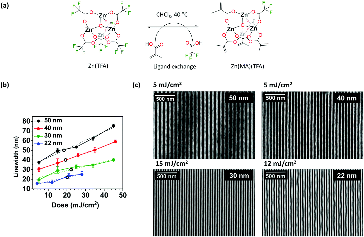 | ||
| Fig. 1 (a) Scheme of Zn(MA)(TFA) synthesis. (b) Dose dependence of line-width of line/space patterns of different half-pitch measured with SEM (2 kV), where grey hollow dots represent the dose-to-size. (c) Selected SEM (5 kV) images of patterned line/space features using EUV-IL. | ||
 | ||
| Scheme 1 Photolithography process and sample fabrication for ex situ spectroscopic analysis performed on Zn(MA)(TFA). | ||
2. Experimental section
2.1 Synthesis of Zn(MA)(TFA) and thin film deposition
The Zn(MA)(TFA) compound was synthesized by ligand exchange from a commercial Zn-oxocluster as precursor having the same tetranuclear oxo-core unit and six TFA ligands, Zn4O(OOCCF3)6, following the protocol in ref. 43 and as shown in Fig. 1a. The deposition of thin films was performed from a Zn(MA)(TFA) solution of 2% (w/v) in a mixture of chloroform (CHCl3), and propylene glycol methyl ether acetate (PGMEA), 9![[thin space (1/6-em)]](https://www.rsc.org/images/entities/char_2009.gif) :1 v/v followed by sonication (4 min) and filtration using a 0.22 μm PTFE filter. Spin-coating of the resist solution was done at 2100 rpm spinning speed (acceleration 3000 rpm s−1) for 30 s. Post application baking was applied for 30 s at 90 °C to remove the excess of the residual solvent. Samples for UV-vis absorption spectroscopy were spin-coated on quartz substrates (500 μm thick) and for FTIR spectroscopy on double-side polished Si substrates (200 μm thick). Samples for X-ray photoelectron spectroscopy (XPS) analysis were spin coated on Cr/Au (3 nm/19 nm) sputter-coated on Si substrate. The thickness of the thin films spin coated for spectroscopic analysis was in the range of 25–30 nm and was measured by using AFM.
:1 v/v followed by sonication (4 min) and filtration using a 0.22 μm PTFE filter. Spin-coating of the resist solution was done at 2100 rpm spinning speed (acceleration 3000 rpm s−1) for 30 s. Post application baking was applied for 30 s at 90 °C to remove the excess of the residual solvent. Samples for UV-vis absorption spectroscopy were spin-coated on quartz substrates (500 μm thick) and for FTIR spectroscopy on double-side polished Si substrates (200 μm thick). Samples for X-ray photoelectron spectroscopy (XPS) analysis were spin coated on Cr/Au (3 nm/19 nm) sputter-coated on Si substrate. The thickness of the thin films spin coated for spectroscopic analysis was in the range of 25–30 nm and was measured by using AFM.
2.2 EUV exposure and development
All EUV exposures were carried out at a wavelength of 13.5 nm (92 eV), at XIL-II beamline of the Swiss Light Source (SLS) synchrotron. For spectroscopic studies open frame 1.7 × 1.7 mm2 area mask and pin-hole (PI), 70 μm was used. For L/S features, the EUVL-IL44 tool was equipped with a transmission mask that resolved half-pitch (HP) of 22, 30, 40, and 50 nm combined with a PI 70 μm. Diluted propionic acid (0.05%) in CHCl3 was used as a developer (8–10 s). Zn(MA)(TFA) behaved as a negative tone photoresist and therefore the exposed areas turn insoluble in the chosen developer. All the mentioned doses in this work are specific to this EUV-IL setup. The tool factors for the specific mask and PI combinations are calculated by cross-calibration with a bench-mark resist material. Thus, this might not correspond to an absolute number and doses might differ slightly when using a different EUV exposure tool.172.3 Post-exposure analysis
UV-vis absorption spectroscopy was performed in a Shimadzu UV2600 spectrophotometer. FTIR spectroscopy of the thin films was performed in transmission mode under vacuum in a Bruker Vertex 80v spectrometer. XPS was performed using a monochromatic AlKα source (1486.6 eV) in an ultra-high vacuum setup (p ≤ 5 × 10⁻⁹ mbar) equipped with Scienta R4000 HiPP-3 analyser. Fitting of the peaks was done using UNIFIT 2018 Scientific software. SEM imaging on L/S features was performed with a top-down view using a FEI Verios 460 operating at a current of 100 pA, dwell time of 10 μs and altering voltage of 5 kV and 2 kV. LWR evaluation was carried out using SMILE, a SEM image analysis software developed at the Paul Scherrer Institute. Unbiased LWRs values46 were obtained using the average power spectral density (PSD) of the lines in their respective SEM images, the unbiasing was performed using a standard PSD model.47 AFM measurements were done using a Bruker Dimensions Icon in ScanAsyst-air mode. As a control experiment, a spectrum of a freshly spin-coated thin film was also used (fresh reference) to inspect the effect of aging/partial degradation of the sample occurring between the exposure and the spectroscopy experiments (as shown in ESI†).3. Results and discussion
To evaluate Zn(MA)(TFA) as a photoresist for EUV lithography, dense L/S patterns on the thin film (22–50 nm) were printed using the EUV-IL tool at the Paul Scherrer Institute.48 SEM images (Fig. 1c) show that the transfer of L/S patterns needed a notably low dose. No scumming (scattered rests of material) between lines was observed. An important aspect in a resist performance is the dose-to-size, which is the incident exposure dose that is needed to attain features of the intended dimension. The plot of printed linewidth as a function of dose for Zn(MA)(TFA) (Fig. 1b)49 showed that the dose-to-size (hollow dots) in all cases is close to 20 mJ cm−2, which is the current requirement for EUV resists. The aspect ratio of the L/S patterns were estimated using the height as measured from the corresponding AFM contour profiles (shown in ESI,† Fig. S1) and found to be ∼1:3 for HP 50 nm, 30 nm, and 22 nm, and ∼1:2 for HP 40 nm. The unbiased LWRs (shown in Fig. 2) of dense L/S features were calculated for the doses of HPs nearest to the printed dose-to-size values (as shown above in Fig. 1b). As a result of line wiggles seen in SEM image of HP 22 nm the results of unbiased LWR are relatively higher. However, the LWR values of the other HP fulfil the industry requirement (LWR < 20% of CD).12 It should be noticed that a good control in the Zn(MA)(TFA) composition is crucial for reproducibility in the sensitivity of this resist.43Table 1 below summarises the performance of some inorganic and hybrid inorganic–organic EUV photoresist when exposed using the EUVL-IL tool at PSI.
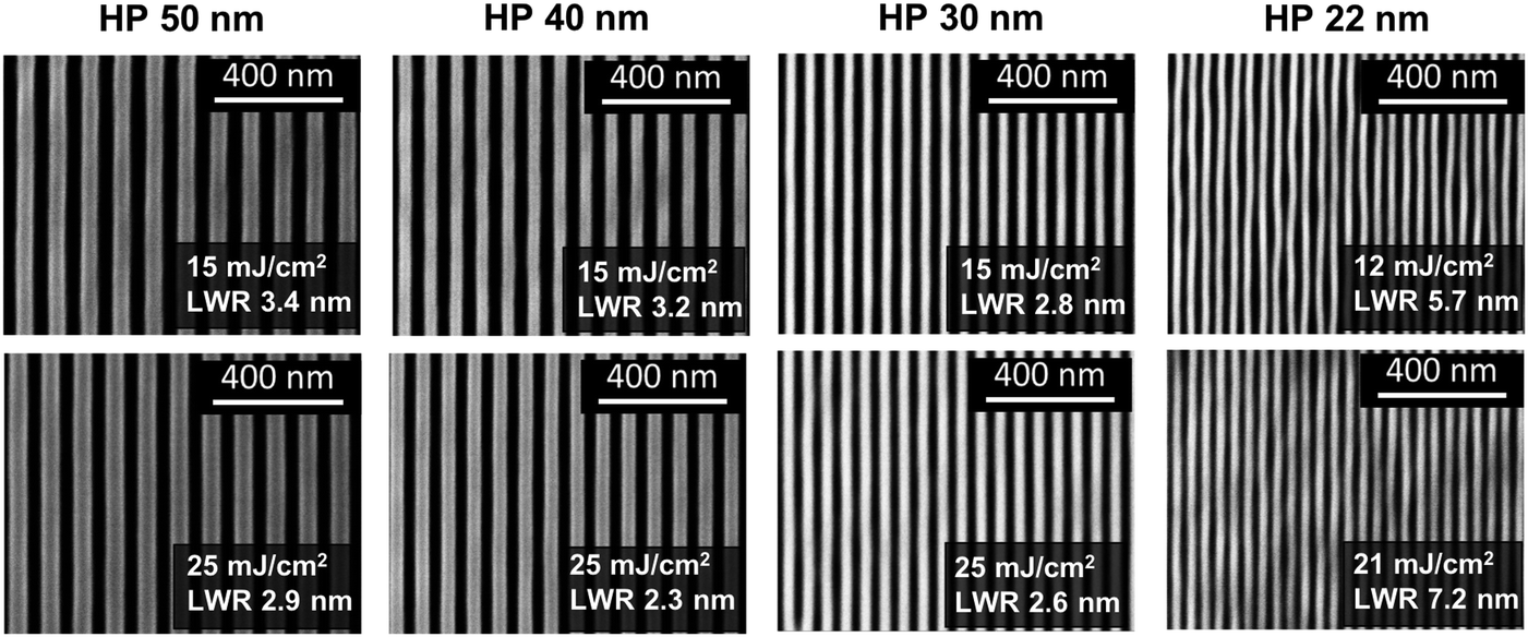 | ||
| Fig. 2 LWR (unbiased) results obtained from PSD of respective SEM (operated at 2 kV) images of line/space features. | ||
| Resist | CD [HP] (nm) | Dose (mJ cm−2) | LWR/LER (nm) | Ref. |
|---|---|---|---|---|
| Inpria YA-BA | 14.9 [16] | 48 | 1.8 | 50 |
| 10 [11] | — | 1.7 | ||
| [(PhSn)12O14(OH)6]Cl2 | [18] | 350 | — | 51 |
| [(BuSn)12O14(OH)6](OH)2 | [50] | 131 | — | 52 |
| [(BuSn)12O14(OH)6](AcO)2 | [40] | 74 | — | 52 |
| HSQ | [22] | 40–90 | ∼2–3 | 53 |
| Zr6O4(OH)4Mc12 | [50] | 57 | — | 30 |
| Zn2(CO2R)4 Zn-mTA | [16] | 45 | — | 26 |
| [13] | 35 | — | ||
| Zn(MA)(TFA) | 30 | 22 | 2.8–2.6 | |
| 22 | 20 | 5.7–7.2 |
The promising outstanding performance of this new material prompted us to investigate the underlying mechanism in the pattern formation. In particular, we wanted to gain insight in the role of each type of ligand in the solubility switch that it undergoes after EUV irradiation. For that purpose, the chemical changes after EUV exposure were investigated with different ex situ spectroscopic techniques. FTIR and UV-vis absorption spectroscopy were employed to identify modifications in the organic ligands, whereas XPS allowed to detect changes in both inorganic and organic components, as it gives information on elemental ratio and on the chemical environment of all elements.
Thin films were exposed to four doses of EUV light from a dose above the threshold necessary to render a fully insoluble thin film (>20 mJ cm−2)43 up to a high dose where a full conversion of the pristine materials is expected, thus allowing the identification of the spectral features from the EUV irradiation product in Zn(MA)(TFA) resist.
A thin film of Zn(MA)(TFA) on Si was exposed to increasing EUV doses on different areas (Fig. 3b) of the same sample and the FTIR of each area was collected (Fig. 3a). The peaks were assigned according to the literature of Zn-based tetranuclear clusters.36,43,54 A decrease in the area of the peaks (Fig. 3c) assigned to the carboxylate groups of both ligands, TFA (νas 1676 cm−1) and MA (νas 1544 cm−1), was detected with increasing dose. The same trend was observed for the peaks assigned to C–F stretching (1205 and 1155 cm−1). However, a relative increase of the peaks in the aliphatic C–H stretching region (2929–2885 cm−1) was observed. This indicates that EUV photons promote the decarboxylation of both TFA and MA. In addition, the simultaneous decrease of the νas(COO) and ν(C–F) peaks suggests that TFA ligands are partially lost, either as complete units or as a result of the ligand fragmentation arising from a decarboxylation process. However, in the case of the MA ligands, the preservation and increase of aliphatic C–H stretching peaks is in line with cross-linking reactions between terminal double bonds.
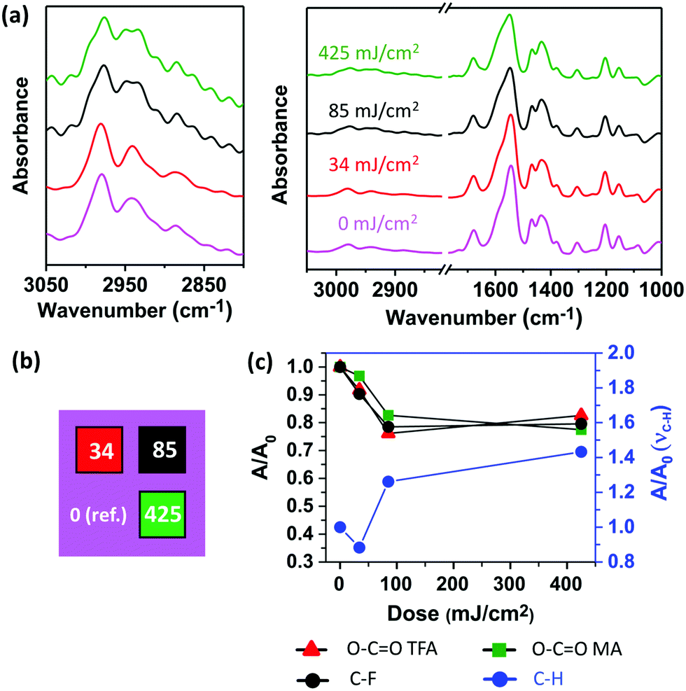 | ||
| Fig. 3 (a) FTIR spectra of a Zn(MA)(TFA) resist film before and after EUV exposure. (b) Scheme of an exposed sample where delimited areas were exposed to different EUV doses (in mJ cm−2). (c) Change in the area of peaks related to MA and TFA ligands as a function of dose relative to the unexposed region. | ||
To further investigate the reactivity of the MA ligands upon EUV exposure we monitored the changes in the UV-vis absorption spectrum of the material after irradiation with different doses of EUV light (Fig. 4). The unexposed material displays an absorption band at 198 nm, which arises from electronic п→п* transition localized in the MA ligands of Zn(MA)(TFA) (Fig. 4a). The bleaching of this band as the EUV dose increases clearly indicates the loss of double bonds with EUV exposure (Fig. 4b). Taking into account that the FTIR experiments confirmed the presence and slight increase of C–H bonds in aliphatic carbons, this result is in line with the promotion of cross-linking reactions between terminal double bonds, which yields saturated carbon chains.24,30
 | ||
| Fig. 4 (a) UV-vis absorption spectra of the resist film and (b) change in the UV-vis absorbance maximum relative to the reference as a function of EUV dose. | ||
As vibrational modes and electronic transitions arising from the inorganic core fall out of the spectroscopic windows in both FTIR and UV-vis experiments, XPS was used to investigate other processes that might occur in the Zn(MA)(TFA) molecule after EUV irradiation. We focused on the detection and tracking of different C, O, F, and Zn-species as the EUV exposure dose increased. To do so, we fitted the C 1s, O 1s, F 1s, and Zn 2p3/2 high resolution spectra for the unexposed material and tracked the species of interest as a function of dose (Fig. 5a and Fig. S5 in ESI†).
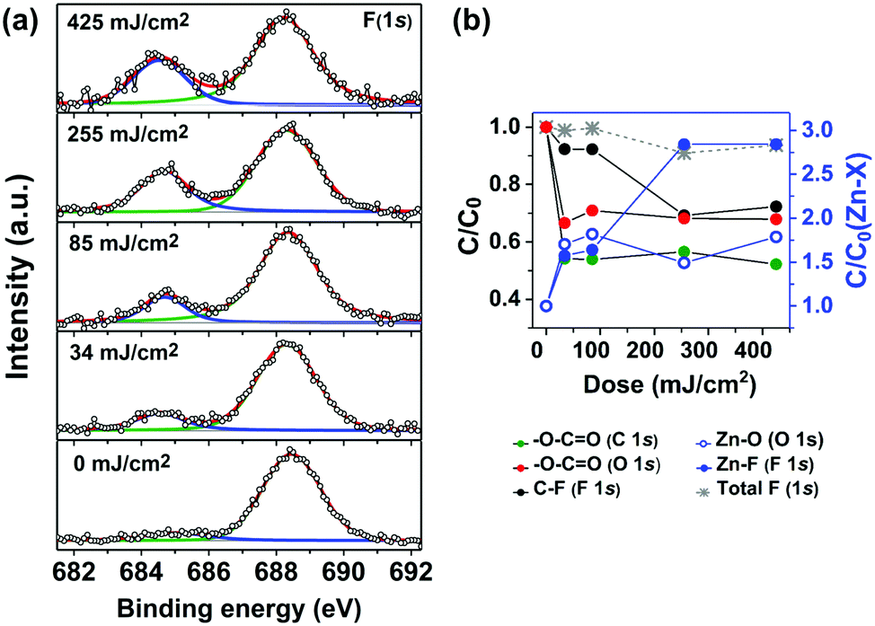 | ||
Fig. 5 (a) Experimental data (dots) and fitting (solid line) of the F 1s high-resolution spectra for unexposed and EUV exposed Zn(MA)(TFA) resist. (b) Changes in the elemental ratio of components of O–C![[double bond, length as m-dash]](https://www.rsc.org/images/entities/char_e001.gif) O (C 1s), O–CO (O 1s) and Zn–O (O 1s) C–F (F 1s), Zn–F (F 1s) and in the total F ratio (F 1s) relative to Zn as a function of EUV dose. O (C 1s), O–CO (O 1s) and Zn–O (O 1s) C–F (F 1s), Zn–F (F 1s) and in the total F ratio (F 1s) relative to Zn as a function of EUV dose. | ||
Although the C 1s spectra could be fitted with 4 components, here we will only consider the components with higher oxidation states, assigned to C atoms in the O–CO groups (289.1 eV) and C atoms bonded to F, C–F (292.8 eV). O 1s spectra were fitted using 2 components, which we attribute to O atoms participating in Zn–O bonds (oxo and hydroxo groups, 532.1 eV) and O atoms in O–CO groups (530.4 eV). A peak assigned to F atoms in the TFA ligands was found in the F 1s accompanied by a small peak with smaller chemical shift (see explanations below). The Zn 2p3/2 peak was fitted using only one component indicating no major chemical differences between the Zn atoms in the inorganic core (see ESI†).
The evolution of the C 1s and O 1s high resolution spectra signified the loss of O–CO species upon EUV exposure (Fig. S5, ESI†), in line with the FTIR results. Yet the most prominent changes were observed in the high-resolution spectra of the F 1s (Fig. 5a). In the latter, it was noticed that the peak at 684.5 eV increases as a function of EUV dose. This peak is assigned to fluoride ions, likely bonded to Zn metal (Zn–F) in the thin film after EUV exposure.55–57 The formation of such metal–fluoride bond has been observed in metal complexes after exposure to focused electron beam and was explained by C–F bond cleavage and appearance of F− species.58 The presence of this peak in low intensity in the unexposed sample is attributed to the chemical changes induced by X-ray photons used for the XPS measurement, as a rise of this peak was observed as a result of prolonged irradiation with X-ray after consecutive measurements on the same spot (Fig. S5, ESI†).
Since our X-ray photoelectron spectrometer does not have spatial resolution, for this experiment each dose required the preparation and exposure of a different sample. Therefore, to track the effect of EUV, we calculated the ratio of each species relative to Zn for each sample and the ratio found at each dose was compared to the initial ratio of each species in the unexposed sample. The ratios relative to Zn 2p3/2 of selected components in C 1s (O–CO), O 1s (O–CO and Zn–O) and F 1s (C–F and Zn–F) spectra were plotted as a function of dose (Fig. 5b). Loss of carboxylate (O–CO, C 1s and O 1s) was detected, yet the contribution of TFA and MA to it cannot be distinguished with this technique, as both carboxylate peaks have the same chemical shift. An increase in Zn–O component as a function of dose was also observed, which can be attributed to the formation of ZnOx species after the EUV exposure. That is, after decarboxylation/ligand loss during exposure, the Zn atoms left in the film can react with water and oxygen in the atmosphere after the samples are taken out of the exposure chamber in the air. As the Zn–F species increase with EUV dose, a decrease in the C–F components is observed, simultaneously. The total concentration of fluorine (grey asterisks in Fig. 5b), decreased by 10% at high EUV doses. Overall, the changes detected in XPS in the fractional ratio with EUV exposure are fairly comparable to the results obtained from FTIR regarding decarboxylation and C–F bond loss.
From the combination of all spectroscopic results, we propose the reactions in Scheme 2 as important contributions to the solubility switch in the Zn(MA)(TFA) resist upon EUV exposure. Ionization of the oxoclusters after absorption of EUV radiation results in the emission of a photoelectron and formation of a radical cation that can further yield the decarboxylation of any of the two types of ligands (reaction (i) in Scheme 2). This process can also be initiated by an electron with kinetic energy higher than the ionization potential of the molecule.59–61 The resulting fragments would be an allyl or a trifluoromethyl radical and an outgassing neutral CO2 molecule. These sites are likely to react with water or oxygen when the film is exposed to ambient atmosphere after EUV exposure and can further lead to aggregation with neighbouring clusters.62–64 Meanwhile, the radicals formed in path (i) can initiate cross-linking reactions of the terminal double bonds in the MA ligands (process (iii) in Scheme 2).
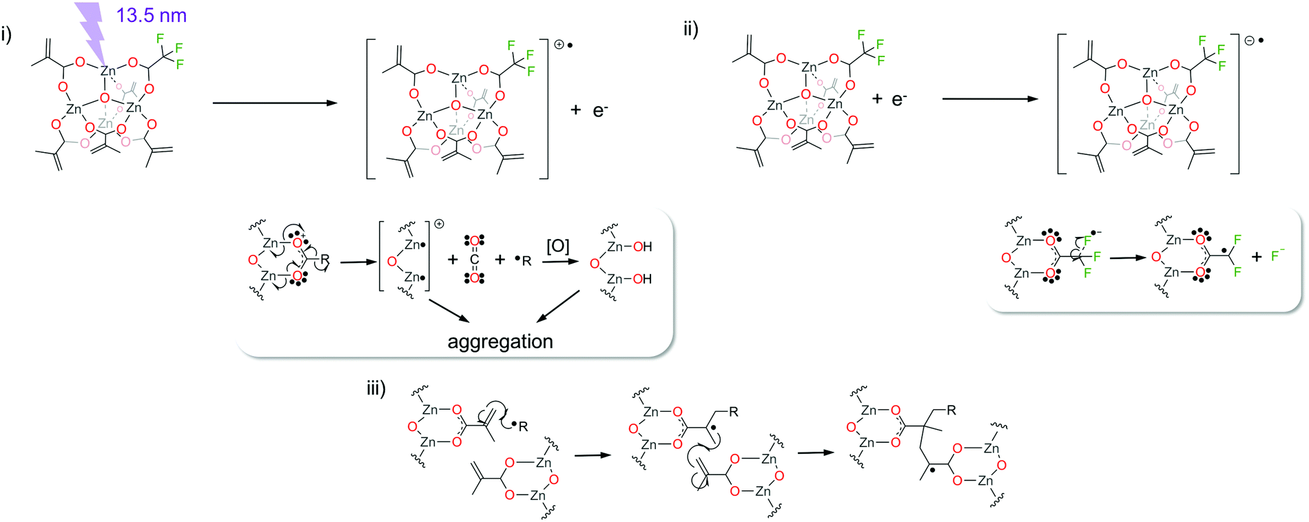 | ||
| Scheme 2 Proposed reaction paths that contribute to the solubility switch in Zn(MA)(TFA) EUV resist. | ||
In addition to dissociative ionization processes, electrons with lower energy than the ionization potential can react with Zn(MA)(TFA) oxocluster and induce the C–F cleavage. This process, known as dissociative electron attachment (DEA), has been reported for halogen-containing molecules and in particular for trifluoroacetic acid.65–69 The resultant fragments would be F− and a difluoroacetyl radical (process (ii) in Scheme 2). Although a detailed structure of the final product cannot be inferred, XPS studies have clearly shown the presence of new F− species in the thin film after EUV exposure. We assume that they are stabilized by the Zn2+ metal cations, as explained above. In turn, the difluoroacetyl radical is expected to react with the neighboring ligands, such as methacrylate ones. Reoxidation of Zn-sites after ligand loss could occur after the exposed sample is exposed to air, as indicated by the XPS studies.
4. Conclusions
The Zn(MA)(TFA) compound has shown the potential to be a competitive material for EUVL applications. EUV interference lithography tests on the Zn(MA)(TFA) resist showed that targeted half-pitch of line/space features for 50 nm, 40 nm, 30 nm and 22 nm can be patterned with a dose of ∼20 mJ cm−2 and unbiased LWR values that comply with the industry requirements. From spectroscopic studies combining FTIR, UV-vis absorption and XPS, we propose a plausible mechanism behind the high sensitivity of this resist that consists of three major reaction paths. One path starts with the ionization and decarboxylation of either the methacrylate or trifluoroacetate ligand to give rise to radical species that can initiate the oligomerization of the terminal double bonds in neighbouring methacrylate ligands. The decarboxylated site, can evolve into hydroxo and oxo species that could bridge neighbouring clusters. Along with these reactions, XPS studies suggest that a third path involves the migration of fluorine atoms from the organic shell to the metal core, most likely promoted by electron attachment. These novel insights into the reaction mechanisms and their correlation to the lithography performance of Zn(MA)(TFA) will help the EUV lithography community to have a better understanding of the molecular design required for new efficient EUV resist materials.Conflicts of interest
There are no conflicts to declare.Acknowledgements
The authors acknowledge the contribution of Najmeh Sadegh for her help with the implementation of the LWR analysis. The research leading to these results has received funding from the European Community's Seventh Framework Programme (FP7/2007-2013) under grant agreement no. 312284 (CALIPSO, 20180993). This work has been carried out within ARCNL, a public–private partnership between University of Amsterdam (UvA), Vrije Universiteit Amsterdam (VU), the Netherlands Organization for Scientific Research (NWO), and ASML.References
- C. Wagner and N. Harned, Nat. Photonics, 2010, 4, 24 CrossRef CAS.
- C. A. Mack, IEEE Trans. Semicond. Manuf., 2011, 24, 202–207 Search PubMed.
- R. M. M. Hasan and X. Luo, Nanomanuf. Metrol., 2018, 1, 67–81 CrossRef.
- A. Lio, Proc. SPIE, 2016, 9776, 97760V Search PubMed.
- M. Neisser, J. Microelectron. Manuf., 2018, 1, 1–8 Search PubMed.
- A. Lio, Synchrotron Radiat. News, 2019, 32, 9–14 CrossRef.
- O. Kostko, B. Xu, M. Ahmed, D. S. Slaughter, D. F. Ogletree, K. D. Closser, D. G. Prendergast, P. Naulleau, D. L. Olynick and P. D. Ashby, J. Chem. Phys., 2018, 149, 154305 CrossRef.
- P. D. Ashby, D. L. Olynick, D. F. Ogletree and P. P. Naulleau, Adv. Mater., 2015, 27, 5813–5819 CrossRef CAS.
- A. Narasimhan, S. Grzeskowiak, B. Srivats, H. C. Herbol, L. Wisehart, C. Kelly, W. Earley, L. E. Ocola, M. Neisser and G. Denbeaux, Proc. SPIE, 2015, 9422, 942208 CrossRef.
- A. Narasimhan, L. Wisehart, S. Grzeskowiak, L. E. Ocola, G. Denbeaux and R. L. Brainard, J. Photopolym. Sci. Technol., 2017, 30, 113–120 CrossRef CAS.
- EUV Lithography, ed. V. Bakshi, SPIE Press, 2018 Search PubMed.
- O. Yildirim, E. Buitrago, R. Hoefnagels, M. Meeuwissen, S. Wuister, G. Rispens, A. van Oosten, P. Derks, J. Finders and M. Vockenhuber, Proc. SPIE, 2017, 10143, 101430Q CrossRef.
- D. De Simone, P. Vanelderen and G. Vandenberghe, J. Photopolym. Sci. Technol., 2017, 30, 613–617 CrossRef CAS.
- R. Fallica, J. Haitjema, L. Wu, S. C. Ortega, A. M. Brouwer and Y. Ekinci, J. Micro/Nanolithogr., MEMS, MOEMS, 2018, 17, 23505 Search PubMed.
- L. Li, X. Liu, S. Pal, S. Wang, C. K. Ober and E. P. Giannelis, Chem. Soc. Rev., 2017, 46, 4855–4866 RSC.
- C. Luo, C. Xu, L. Lv, H. Li, X. Huang and W. Liu, RSC Adv., 2020, 10, 8385–8395 RSC.
- X. Wang, Z. Tasdemir, I. Mochi, M. Vockenhuber, L. van Lent-Protasova, M. Meeuwissen, R. Custers, G. Rispens, R. Hoefnagels and Y. Ekinci, Proc. SPIE, 2019, 10957, 109570A Search PubMed.
- M. Trikeriotis, M. Krysaki, Y. S. Chung, C. Ouyang, B. Cardineau, R. Brainard, C. K. Ober, E. P. Giannelis and K. Cho, J. Photopolym. Sci. Technol., 2012, 25, 583–586 CrossRef CAS.
- M. E. Krysak, J. M. Blackwell, S. E. Putna, M. J. Leeson, T. R. Younkin, S. Harlson, K. Frasure and F. Gstrein, Proc. SPIE, 2014, 9048, 904805 CrossRef.
- R. Del, Re, J. Passarelli, M. Sortland, B. Cardineau, Y. Ekinci, E. Buitrago, M. Neisser, D. A. Freedman and R. L. Brainard, J. Micro/Nanolithogr., MEMS, MOEMS, 2015, 14, 43506 CrossRef.
- H. Xu, K. Sakai, K. Kasahara, V. Kosma, K. Yang, H. C. Herbol, J. Odent, P. Clancy, E. P. Giannelis and C. K. Ober, Chem. Mater., 2018, 30, 4124–4133 CrossRef CAS.
- B. Cardineau, R. Del Re, H. Al-Mashat, M. Marnell, M. Vockenhuber, Y. Ekinci, C. Sarma, M. Neisser, D. A. Freedman and R. L. Brainard, Proc. SPIE, 2014, 9051, 90511B CrossRef.
- L. Wu, M. Vockenhuber, Y. Ekinci and S. Castellanos, Proc. SPIE, 2019, 10957, 109570B Search PubMed.
- E. C. Mattson, Y. Cabrera, S. M. Rupich, Y. Wang, K. A. Oyekan, T. J. Mustard, M. D. Halls, H. A. Bechtel, M. C. Martin and Y. J. Chabal, Chem. Mater., 2018, 30, 6192–6206 CrossRef CAS.
- L. Wu, J. Liu, M. Vockenhuber, Y. Ekinci and S. Castellanos, Eur. J. Inorg. Chem., 2019, 4136–4141 CrossRef CAS.
- H. Xu, K. Sakai, K. Kasahara, V. Kosma, K. Yang, H. C. Herbol, J. Odent, P. Clancy, E. P. Giannelis and C. K. Ober, Chem. Mater., 2018, 30, 4124–4133 CrossRef CAS.
- A. De Silva, N. M. Felix and C. K. Ober, Adv. Mater., 2008, 20, 3355–3361 CrossRef CAS.
- H. Xu, V. Kosma, K. Sakai, E. P. Giannelis and C. K. Ober, J. Micro/Nanolithogr., MEMS, MOEMS, 2018, 18, 11007 Search PubMed.
- R. Maas, M.-C. van Lare, G. Rispens and S. F. Wuister, J. Micro/Nanolithogr., MEMS, MOEMS, 2018, 17, 41003 CAS.
- L. Wu, M. Baljozovic, G. Portale, M. Vockenhuber, T. Jung, Y. Ekinci and S. Castellanos, J. Micro/Nanolithogr., MEMS, MOEMS, 2019, 18, 013504 CAS.
- L. Wu, M. Tiekink, A. Giuliani, L. Nahon and S. Castellanos, J. Mater. Chem. C, 2019, 7, 33 RSC.
- C. S. McCowan, T. L. Groy and M. T. Caudle, Inorg. Chem., 2002, 41, 1120–1127 CrossRef CAS.
- W. Clegg, D. R. Harbron, C. D. Homan, P. A. Hunt, I. R. Little and B. P. Straughan, Inorganica Chim. Acta, 1991, 186, 51–60 CrossRef CAS.
- R. M. Gordon and H. B. Silver, Can. J. Chem., 1983, 61, 1218–1221 CrossRef CAS.
- P. Cubillas, K. Etherington, M. W. Anderson and M. P. Attfield, CrystEngComm, 2014, 16, 9834–9841 RSC.
- S. B. Ötvös, O. Berkesi, T. Körtvélyesi and I. Pálinkó, Inorg. Chem., 2010, 49, 4620–4625 CrossRef.
- N. L. Rosi, J. Eckert, M. Eddaoudi, D. T. Vodak, J. Kim, M. O’Keeffe and O. M. Yaghi, Science, 2003, 300, 1127–1129 CrossRef CAS.
- M. D. Christianson, M. M. Meyer, O. Ongayi, D. Valeri and M. Wagner, Proc. SPIE, 2013, 8682, 868216 CrossRef.
- M. Carraro and S. Gross, Materials, 2014, 7, 3956–3989 CrossRef CAS.
- I. Erukhimovich and M. O. de la Cruz, J. Polym. Sci., Part B: Polym. Phys., 2004, 45, 2215–2231 Search PubMed.
- U. Schubert, Chem. Soc. Rev., 2011, 40, 575–582 RSC.
- U. Schubert, Chem. Mater., 2001, 13, 3487–3494 CrossRef CAS.
- N. Thakur, L.-T. Tseng, M. Vockenhuber, Y. Ekinci and S. Castellanos, J. Micro/Nanolithogr., MEMS, MOEMS, 2019, 18, 43504 CAS.
- N. Mojarad, J. Gobrecht and Y. Ekinci, Microelectron. Eng., 2015, 143, 55–63 CrossRef CAS.
- N. Mojarad, D. Fan, J. Gobrecht and Y. Ekinci, Opt. Lett., 2014, 39, 2286–2289 CrossRef CAS.
- G. F. Lorusso, T. Sutani, V. Rutigliani, F. Van Roey, A. Moussa, A.-L. Charley, C. Mack, P. Naulleau, C. Perera and V. Constantoudis, J. Micro/Nanolithogr., MEMS, MOEMS, 2018, 17, 41009 Search PubMed.
- G. Palasantzas, Phys. Rev. B: Condens. Matter Mater. Phys., 1993, 48, 14472–14478 CrossRef CAS.
- I. Mochi and Y. Ekinci, Synchrotron Radiat. News, 2019, 32, 22–27 CrossRef.
- C. Mack, Fundamental Principles of Optical Lithography: The Science of Microfabrication, John Wiley & Sons, 2008 Search PubMed.
- A. Grenville, J. T. Anderson, B. L. Clark, P. De Schepper, J. Edson, M. Greer, K. Jiang, M. Kocsis, S. T. Meyers, J. K. Stowers, A. J. Telecky, D. De Simone and G. Vandenberghe, Proc. SPIE, 2015, 9425, 94250S CrossRef.
- B. Cardineau, R. Del Re, M. Marnell, H. Al-Mashat, M. Vockenhuber, Y. Ekinci, C. Sarma, D. A. Freedman and R. L. Brainard, Microelectron. Eng., 2014, 127, 44–50 CrossRef CAS.
- J. Haitjema, Y. Zhang, M. Vockenhuber, D. Kazazis, Y. Ekinci and A. M. Brouwer, J. Micro/Nanolithogr., MEMS, MOEMS, 2017, 16, 033510 Search PubMed.
- T. Gädda, L. N. Dang, M. Laukkanen, K. Karaste, O. Kähkönen, E. Kauppi, D. Kazazis, Y. Ekinci and J. T. Rantala, Proc. SPIE, 2019, 10960, 109600B Search PubMed.
- R. Chen, Y. Li, L. Tang, H. Yang, Z. Lu, J. Wang, L. Liu and K. Takahashi, RSC Adv., 2017, 7, 40020–40027 RSC.
- M. Sportelli, M. Valentini, R. Picca, A. Milella, A. Nacci, A. Valentini and N. Cioffi, Appl. Sci., 2018, 8, 77 CrossRef.
- Y. Kawamoto, K. Ogura, M. Shojiya, M. Takahashi and K. Kadono, J. Fluorine Chem., 1999, 96, 135–139 CrossRef CAS.
- E. Polydorou, A. Zeniou, D. Tsikritzis, A. Soultati, I. Sakellis, S. Gardelis, T. A. Papadopoulos, J. Briscoe, L. C. Palilis and S. Kennou, J. Mater. Chem. A, 2016, 4, 11844–11858 RSC.
- S. G. Rosenberg, M. Barclay and D. H. Fairbrother, ACS Appl. Mater. Interfaces, 2014, 6, 8590–8601 CrossRef CAS.
- L. Wu, M. Tiekink, A. Giuliani, L. Nahon and S. Castellanos, J. Mater. Chem. C, 2019, 7, 33–37 RSC.
- K. Ahlenhoff, S. Koch, D. Emmrich, R. Dalpke, A. Gölzhäuser and P. Swiderek, Phys. Chem. Chem. Phys., 2019, 21, 2351–2364 RSC.
- F. Lebreux, F. Buzzo and I. Marko, ECS Trans., 2008, 13, 1–10 CAS.
- C.-C. Yeh, H.-C. Liu, W. Heni, D. Berling, H.-W. Zan and O. Soppera, J. Mater. Chem. C, 2017, 5, 2611–2619 RSC.
- F. Stehlin, F. Wieder, A. Spangenberg, J.-M. Le Meins and O. Soppera, J. Mater. Chem. C, 2014, 2, 277–285 RSC.
- L. Li, S. Chakrabarty, K. Spyrou, C. K. Ober and E. P. Giannelis, Chem. Mater., 2015, 27, 5027–5031 CrossRef CAS.
- M. Zawadzki, A. Chachereau, J. Kočišek, C. M. Franck and J. Fedor, J. Chem. Phys., 2018, 149, 204305 CrossRef CAS.
- J. P. Wiens, J. C. Sawyer, T. M. Miller, N. S. Shuman, A. A. Viggiano, M. Khamesian, V. Kokoouline and I. I. Fabrikant, Phys. Rev. A: At., Mol., Opt. Phys., 2016, 93, 32706 CrossRef.
- J. Langer, M. Stano, S. Gohlke, V. Foltin, S. Matejcik and E. Illenberger, Chem. Phys. Lett., 2006, 419, 228–232 CrossRef CAS.
- M. Orzol, T. Sedlacko, R. Balog, J. Langer, G. P. Karwasz, E. Illenberger, A. Lafosse, M. Bertin, A. Domaracka and R. Azria, Int. J. Mass Spectrom., 2006, 254, 63–69 CrossRef CAS.
- E. Böhler, J. Warneke and P. Swiderek, Chem. Soc. Rev., 2013, 42, 9219–9231 RSC.
Footnote |
| † Electronic supplementary information (ESI) available. See DOI: 10.1039/d0tc03597a |
| This journal is © The Royal Society of Chemistry 2020 |