
 Open Access Article
 This Open Access Article is licensed under a
 Creative Commons Attribution 3.0 Unported Licence
Thiol–yne crosslinked triarylamine hole transport layers for solution-processable organic light-emitting diodes†
Ksenia
Kutonova‡
ab,
Bernd
Ebenhoch‡
ac,
Lorenz
Graf von Reventlow
ac,
Stefan
Heißler
d,
Lukas
Rothmann
c,
Stefan
Bräse
*abe and
Alexander
Colsmann
 *ac
*ac
aMaterial Research Center for Energy Systems (MZE), Karlsruhe Institute of Technology, Strasse am Forum 7, 76131 Karlsruhe, Germany. E-mail: stefan.braese@kit.edu; alexander.colsmann@kit.edu
bInstitute of Organic Chemistry (IOC), Karlsruhe Institute of Technology (KIT), Fritz-Haber-Weg 6, 76131 Karlsruhe, Germany
cLight Technology Institute (LTI), Karlsruhe Institute of Technology, Engesserstrasse 13, 76131 Karlsruhe, Germany
dInstitute of Functional Interfaces (IFG), Karlsruhe Institute of Technology (KIT), Hermann-von-Helmholtz-Platz 1, 76344 Eggenstein-Leopoldshafen, Germany
eInstitute of Biological and Chemical Systems (IBCS-FMS), Karlsruhe Institute of Technology (KIT), Hermann-von-Helmholtz-Platz 1, 76344 Eggenstein-Leopoldshafen, Germany
First published on 22nd October 2020
Abstract
Triarylamine derivatives are widely used for hole transport in organic optoelectronic devices, but their excellent solubility in many common solvents limits their use for multi-layer device fabrication from solution. In this work, a novel process to the formation of conjugated triarylamine polymer thin-film networks by crosslinking of thiol-substituted and alkyne-substituted triarylamines is investigated. After deposition of the monomer blend and crosslinking under UV exposure, an insoluble thiol–yne polymer network is formed. The applicability of the thiol–yne polymer network as hole-transport layers is exemplified on organic light-emitting diodes. Its implementation reduces the device degradation as compared to OLEDs comprising hole-transport layers from PEDOT:PSS.
Introduction
Advanced and efficient organic light-emitting diodes (OLEDs) require elaborated multi-layer device architectures. Today, most of the commercially available OLEDs and displays thereof are fabricated by thermal evaporation of molecular semiconductors in a vacuum. Future advancements of this technology are expected from solution-processing in versatile (digital) printing processes, such as inkjet printing, simultaneously lowering material consumption and process energy while increasing process flexibility.1,2 As of today, the subsequent deposition of multiple functional layers from solution is a non-trivial task. The use of orthogonal solvents which prevent the dissolution of any previously applied layers is currently the most often implemented strategy. Although sophisticated layer stacks with up to nine functional layers, processed from solution, have been realized using orthogonal solvents,3 the concept naturally limits the choice of semiconductors. In particular, the applicability of smaller semiconducting molecules is limited by their good solubility in most aromatic solvents that are also used to deposit common emission layers.Triarylamine derivatives, featuring their efficient oxidation occurring at the nitrogen center, their intrinsic electron-donating nature and their ability to transport holes via formation of relatively stable radical cations, are nowadays widely used as hole transport layers (HTLs).4–14 Due to their excellent solubility in many organic solvents, their applicability in multi-layer solution-processed OLEDs is limited.
To achieve insoluble HTLs for multi-layer architectures, crosslinking is a promising way forward.15–22 A wide range of crosslinking reactions suitable for the synthesis of triarylamine-containing polymers was reported, including light-induced21 or heat-induced23 [2+2] cycloaddition, acrylate24–28 or styrene29–33 side-chain free-radical polymerization, anionic living polymerization,34,35 siloxane condensation,36–39 Schiff bases polycondensation,40 electrochemical oxidative polymerization,41–43 diyne polycyclotrimerization44 and polycondensation of bisphenols or biscarbamates with aryl or alkylhalogenides45,46 or diamines with diacid chlorides.47 A range of metal-catalyzed reactions, such as Cu(I)-catalyzed azide–alkyne click reaction,48 Pd-catalyzed Buchwald–Hartwig amination49,50 and Suzuki crosscoupling,51–53 Ullmann reaction54,55 as well as ring-opening metathesis56–58 was also successfully used for the synthesis of polymers containing triarylamine units, both as bulk material and as thin films.
Yet, crosslinking reactions must comply with a number of further requirements to be implementable in optoelectronic devices. Ideally, the synthetic procedures are metal-free, as residues of metals can impact on the performance of the respective devices due to metal–organic interactions.44,59,60 Byproducts from the crosslinking reaction can act as unwanted dopants or recombination centers or may evaporate during the crosslinking reaction and lead to the formation of porous films – all of which can negatively influence the electronic properties of the thin films and, therefore, should be avoided. Crosslinking via conjugated bonds is preferred over long aliphatic chains, as the latter can significantly reduce the charge carrier mobility by spacing,15,61 whereas an increased conjugation length generally enhances the hole mobility.62 Therefore, the development of conjugated HTLs is highly desirable.63–65 Remaining reaction sites of the monomers can act as charge carrier traps and thus the crosslinking reaction should ideally approach a conversion of 100%. Beyond changing the solubility, crosslinking enables the formation of robust HTLs with high glass transition temperatures and thus prevents morphological changes. Crosslinking can, therefore, also be a valuable technique to increase the long-term stability of optoelectronic devices.9,22 To enable processing on flexible, temperature-sensitive substrates, the crosslinking reaction can be triggered by UV exposure.
Here we report on the synthesis of thiol- and alkyne-substituted triarylamines, the formation of conjugated crosslinked thin films and their implementation as HTLs in OLEDs followed by an analysis of performance and degradation. The crosslinked thin films are synthesized by deposition of a blend of thiol- and alkyne-substituted triarylamines directly onto the bottom electrode. The thiol–yne reaction is then initiated and controlled by UV exposure, it proceeds without the development of byproducts and leads to the formation of an insoluble conjugated polymer network thin film, which allows the deposition of subsequent layers from aromatic solvents. We study the crosslinking reaction in thin films by attenuated total reflectance Fourier-transform infrared spectroscopy (ATR-FTIR) and investigate the semiconductor properties by absorption spectroscopy, photoelectron yield spectroscopy in air and the hole mobility by space charge limited currents.
Results and discussion
Synthesis
The monomers tris(4-ethynylphenyl)amine 3 and tris(4-thiyphenyl)amine 5 were synthesized as shown in Scheme 1. The synthesis of alkyne 3 was performed starting from tris(4-iodophenyl)amine 1, which was coupled with trimethylsilylacetylene (TMS acetylene) using the Sonogashira cross-coupling reaction,66 followed by deprotection of the obtained tris(4-((trimethylsilyl)ethynyl)phenyl)amine 2 by tetrabutylammonium fluoride.67 Thiol 5 was obtained in two steps: the reaction of tris(4-bromophenyl)amine 4 with sodium isopropylthiolate NaSiPr, leading to the formation of a thioether, and its further conversion to the target tris(4-thiyphenyl)amine 5 by heating the reaction mixture with elemental sodium. | ||
| Scheme 1 Synthesis of tris(4-ethynylphenyl)amine 3 and tris(4-thiyphenyl)amine 5. | ||
Thin film blends of the two monomers tris(4-ethynylphenyl)amine 3 and tris(4-thiyphenyl)amine 5 were crosslinked under UV exposure, resulting in the hole-transport polymer network 6 (Scheme 2). The thin films were spin-coated from blend solutions of alkyne 3 and thiol 5 (molar ratio 1![[thin space (1/6-em)]](https://www.rsc.org/images/entities/char_2009.gif) :1) in THF on quartz glass substrates. The resulting as-cast films, with a thickness of 59 nm, were exposed to UV radiation (365 nm, 1 mW cm−2, 2 hours) triggering the thiol–yne reaction to form a polymer network. Due to the twisted propeller-like geometry of alkyne 3 and thiol 5, the polymer network 6 is expected to be highly amorphous. The obtained polymer coating is insoluble in common organic solvents. Even after sonication in THF, chloroform and chlorobenzene, no changes in surface texture and roughness were observed in optical microscopy.
:1) in THF on quartz glass substrates. The resulting as-cast films, with a thickness of 59 nm, were exposed to UV radiation (365 nm, 1 mW cm−2, 2 hours) triggering the thiol–yne reaction to form a polymer network. Due to the twisted propeller-like geometry of alkyne 3 and thiol 5, the polymer network 6 is expected to be highly amorphous. The obtained polymer coating is insoluble in common organic solvents. Even after sonication in THF, chloroform and chlorobenzene, no changes in surface texture and roughness were observed in optical microscopy.
 | ||
| Scheme 2 Formation of the polymer network 6 by thiol–yne reaction of 3 and 5, initiated by UV exposure. | ||
To confirm the thiol–yne reaction, the obtained polymer thin-film networks were studied by ATR-FTIR spectroscopy. While in the IR spectra of the initial alkyne 3 and thiol 5, the characteristic absorption bands corresponding to the C–H stretching of alkyne 3 (3290 cm−1) and S–H stretching of thiol 5 (2551 cm−1) were observed, these bands almost disappeared in the IR spectra of the polymer 6 (see ESI,† Fig. S5). ATR-FTIR was also used to estimate the kinetics of the reaction and the crosslinking degree by monitoring the conversion over time. Therefore, a UV source was mounted onto the spectrometer and ATR-FTIR spectra were recorded at 0 min (as-cast films, no UV exposure), and then the measurement was repeated ten times, each after 5 min of UV exposure. The obtained ATR-FTIR spectra in Fig. 1a were normalized to the SiO2 absorption band (919 cm−1) and plotted as a function of exposure time. The intensity of the band, corresponding to the C–H bond stretching of alkyne 3 (3290 cm−1) in Fig. 1b significantly decreased already after 5 min of UV exposure and reached a plateau after 45 min. Based on the intensity of this band before and after polymerization, we estimated that 90% of the alkyne-groups reacted during the polymerization. In the blend films, the intensity of the band corresponding to the S–H stretching of thiol 5 was too low to be monitored. In addition, two trends, related to the phenyl ring vibrations (C–C stretching modes) were identified: an increased absorbance of the band at 1590 cm−1 (as ν8a and ν8b degenerate in-plane ring vibrations, due to the extended conjugation with π-electrons of the formed C![[double bond, length as m-dash]](https://www.rsc.org/images/entities/char_e001.gif) C bond and lone-pairs of sulfur atoms) and a significant decrease of the band intensity at 1490 cm−1 (as ν19a and ν19b degenerate in-plane ring vibrations, due to the decrease of the molecular degrees of freedom). Both effects evidence that the thiol–yne reaction led to the formation of a conjugated polymer network.
C bond and lone-pairs of sulfur atoms) and a significant decrease of the band intensity at 1490 cm−1 (as ν19a and ν19b degenerate in-plane ring vibrations, due to the decrease of the molecular degrees of freedom). Both effects evidence that the thiol–yne reaction led to the formation of a conjugated polymer network.
 | ||
| Fig. 1 Time-dependent ATR-FTIR spectra of the thiol-alkyne blend under UV exposure (365 nm, 0.5 mW cm−2). (a) 3-D representation of the absorbance spectra in the IR spectral regime as a function of UV exposure time. (b) Relative intensity of bands at 3290 cm−1, 1590 cm−1 and 1490 cm−1versus UV exposure time. | ||
The thiol–yne crosslinking strategy also significantly increases the thermal stability of polymer 6 compared to alkyne 3 and thiol 5 as demonstrated by differential scanning calorimetry (DSC) (see ESI,† Fig. S6). Alkyne 3 and thiol 5 have melting points at 98 °C and 130 °C, respectively. Additionally, an exothermic event was observed for alkyne 3 at temperatures above 100 °C which is assigned to alkyne 3 polymerization, as an insoluble material was formed after the DSC analysis. The DSC curve of the thiol–yne polymer 6 shows no thermal events upon heating to 180 °C, proving its thermal stability.
Optoelectronic properties
According to the absorbance spectrum in Fig. 2a, blend films of alkyne 3 and thiol 5 are widely transparent in the visible spectral regime with a prominent absorption peak in the UV at 340 nm. This is an important asset to avoid parasitic absorption when implemented as HTLs in OLEDs. Upon crosslinking, the absorption spectrum broadens, the peak absorption is reduced and the absorption at the tail is enhanced. The absorption peak is slightly red-shifted by 5 nm upon crosslinking. This red-shift and the broadening of the absorption may be attributed to an increased conjugation length.17 The persistence of the absorbance of the sample in the inset of Fig. 2a after crosslinking of the thin film, before and after sonication in THF confirms that the film became insoluble.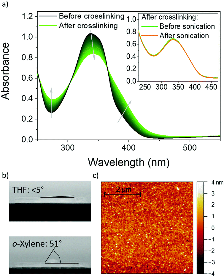 | ||
| Fig. 2 (a) The absorbance of blends of alkyne 3 and thiol 5 in thin films (86 nm thickness). Inset: The absorbance of the crosslinked polymer 6 layer before and after sonication in THF. (b) The contact angles of THF (top, 5°) and o-xylene (bottom, 51°) with the polymer 6 thin-film surface. (c) The topography of a representative polymer 6 layer. | ||
For the subsequent deposition of further functional layers from solution, a good wettability of the surface is required. As depicted in Fig. 2b, THF and o-xylene form contact angles of less than 5° and 51° on the crosslinked layers, indicating good wettability of these organic solvents that are commonly used to deposit subsequent functional layers (e.g. emission layers), without dissolving the polymer 6 network. Furthermore, the atomic force microscope image in Fig. 2c reveals a very smooth thin-film surface with a root-mean-square roughness of less than 1 nm.
For the implementation as HTL into organic optoelectronic devices and the formation of good electrical contacts with the electrodes, the transport energies are crucially important. The ionization energies were determined by photoelectron yield spectroscopy in air (PESA) on thin films. As depicted in Fig. 3, the ionization energies of alkyne 3 and thiol 5 are 5.9 eV and 5.7 eV. The lower ionization energy of thiol 5 is well in agreement with the electronic substituents effect, as the electron donating –SH group increases the electron density on the aromatic system and the central nitrogen atom, and thus raises the HOMO of the molecule (in contrast to the electron withdrawing –C![[triple bond, length as m-dash]](https://www.rsc.org/images/entities/char_e002.gif) CH group). The ionization energy of the polymer 6 is 5.8 eV and hence between the ionization energies of alkyne 3 and thiol 5.
CH group). The ionization energy of the polymer 6 is 5.8 eV and hence between the ionization energies of alkyne 3 and thiol 5.
 | ||
| Fig. 3 Ionization energies of alkyne 3, thiol 5 and polymer 6, determined by PESA on solid-state thin films. | ||
To be suitable for the implementation as HTL into OLEDs, sufficiently high hole mobilities and conductivities are required. Here, the hole conductivities and mobilities were measured in ‘hole-only devices’, where two high-work-function electrodes ensure the lossless injection of holes and prevent the injection of electrons into polymer 6 thin films. Therefore, as depicted in the inset of Fig. 4, a sufficiently thick polymer 6 layer (86 nm) was washed with THF and sandwiched between nickel oxide (NiOx) and molybdenum trioxide (MoO3) hole injection layers. Fig. 4 shows representative current density–voltage (J–V) curves of the samples under positive and negative bias, injecting holes from MoO3 and NiOx, respectively. The strong similarity of the curves indicates that the shape of the J–V curve is governed by bulk effects rather than injection barriers. In case of ohmic contacts, beyond an ohmic regime at lower voltages, the J–V sweep produces space-charges within the sample and the J–V characteristics can be described by an extended Mott–Gurney law, where d represents the layer thickness and ε0 the vacuum permittivity.
 | (1) |
 | ||
| Fig. 4 J–V sweeps under positive and negative bias of hole-only devices comprising the crosslinked polymer 6 (layer thickness 86 nm) sandwiched between MoO3 and NiOx. Open symbols indicate hole-injection through NiOx, closed symbols indicate hole-injection through MoO3, the solid line represents the model fit according to eqn (1). The inset depicts the architecture of the hole-only devices. | ||
By assuming a relative permittivity εr ≈ 3, the hole mobility (μh) and conductivity (σh) are the only unknown variables.68 By fitting the data in Fig. 4 with eqn (1), a hole mobility μh = 2 × 10⁻⁸ cm2 V−1 s−1 and a hole conductivity σh = 5 × 10⁻¹¹ S cm−1 of the polymer 6 were obtained. Although at the lower end of the regime, the hole conductivity of polymer 6 is comparable to other triarylamines such as 4,4′,4′′-tris[phenyl(m-tolyl)amino]triphenylamine (m-MTDATA) which are often implemented as HTL in OLEDs.69 The somewhat reduced hole mobility is likely to stem from the high degree of crosslinking within the polymer network, inducing some disorder.
OLEDs
Upon integration as HTL into OLEDs, polymer 6 shows its versatile properties. Fig. 5a depicts the OLED architecture comprising the emitter (4s,6s)-2,4,5,6-tetra(9H-carbazol-9-yl)isophthalonitrile (4CzIPN), which belongs to the family of thermally activated delayed fluorescence (TADF) emitters, embedded in a 4,4′-di(N-carbazolyl)biphenyl (CBP) host (5 wt%, 4 g L−1 in THF). The HTLs and the emission layers were deposited from solution to demonstrate the advantages of the crosslinked and insoluble polymer 6. All other functional layers were deliberately vacuum-processed to enhance the reproducibility and comparability of the OLED performance across the different OLEDs. Electron injection was facilitated by thermally evaporated bis-4,6-(3,5-di-4-pyridylphenyl)-2-methylpyrimidine (B4PyMPM) and 8-hydroxyquinolatolithium (Liq) electron-transport layers, followed by an aluminum electrode. For reference, we also fabricated OLEDs comprising electrically doped PEDOT:PSS as HTL which is often used in state-of-the-art devices. | ||
| Fig. 5 (a) Device architecture of the OLEDs under investigation. (b) The L–V (solid lines) and J–V curves (dotted lines) show almost identical shapes. Von increases towards thicker polymer 6 layers. (c) The EQEs of all devices show negligible roll-off. Best EQEs are achieved for thin polymer 6 layers. (d) Power efficiency of the OLEDs. (e) The emission spectra slightly broaden for an increasing thickness of polymer 6. (f) Degradation of the OLEDs versus time: driving voltage. (g) The implementation of polymer 6 significantly reduces the decline of the EQE over time. (h) After 20 min of operation, the power efficiency of the reference OLEDs comprising PEDOT:PSS match the power efficiency of optimized OLEDs incorporating polymer 6. | ||
Fig. 5b depicts the luminance L and the current density J versus voltage V (L–V and J–V) of OLEDs comprising HTLs of polymer 6 with layer thicknesses in the range of 8 to 86 nm. All OLED characteristics were measured up to a luminance of L = 800 cd m−2 to comply with the brightness requirements of most display applications. Both L–V and J–V are identical in shape, which indicates negligible parasitic currents and small external quantum efficiency (EQE) roll-offs as confirmed in the EQE versus luminance plot in Fig. 5c. Best OLED performance was achieved for HTL layer thicknesses of 8 nm and 17 nm. Commonly, thin functional layers with a thickness below 20 nm are prone to shunts, in particular when depositing subsequent layers from solution. Here, polymer 6, being a robust and dense crosslinkable triarylamine polymer, can make an important difference, enabling also thin HTLs.
Incorporating polymer 6 at the optimized layer thickness of 17 nm produced OLEDs with an onset voltage versus luminance Von,L = 3.3 V (voltage at 1 cd m−2) which comes close to the reference OLEDs with HTLs from PEDOT:PSS (Von,L = 2.7 V), although polymer 6 is not electrically doped. The onset voltage of the exponential rise of the current density for all OLEDs is about Von,J = 2.5 V, evidencing that the injection of holes is similarly efficient for PEDOT:PSS and polymer 6. At larger thicknesses, Von,L drastically increases due to ohmic resistance, stemming from the lower conductivity of polymer 6. As a consequence, the OLEDs comprising the reference HTL PEDOT:PSS outperform the OLEDs that incorporate HTLs from polymer 6, which is summarized in the power efficiency versus luminance plot in Fig. 5d. We note that we observed only a minor broadening in the emission spectrum in dependence on the polymer 6 layer thickness (Fig. 5e) which may stem from minor cavity effects or small shifts of the recombination zone within the emission layer. The Commission Internationale de l’Eclairage (CIE 1931 xy) color coordinates shift slightly from 0.28, 0.55 to 0.26, 0.57 for increasing thicknesses of the polymer 6 layer (see ESI,† Table S7).
Yet, a completely different picture is drawn when assessing the long-term stability of the devices. Fig. 5f–h compare the degradation of OLEDs comprising HTLs of either polymer 6 or PEDOT:PSS. The OLEDs were measured in a nitrogen-filled glove box over a period of 20 minutes at a constant current of 0.95 mA cm−2, which corresponds to an initial luminance of approximately 300–400 cd m−2. Most notably, the EQE of the OLEDs with HTLs of PEDOT:PSS in Fig. 5g shows a significant relative decrease of more than 50% over 20 minutes (from initially 14% to less than 7% absolute) which may originate from its known acidity and the concomitant release of ions from the ITO electrode.70 In contrast, the EQEs of the OLEDs comprising polymer 6 HTLs decay much slower. After a few minutes only, all OLEDs with polymer 6 HTLs exhibit higher EQEs than the PEDOT:PSS reference devices since, even in this rather simple device architecture, their degradation is much more retarded.
Conclusions
We have introduced thiol–yne reactions as a crosslinking mechanism to obtain novel, highly robust and insoluble triarylamine layers from solution. The thiol–yne reaction is initiated by UV exposure and leads to a conjugated polymer network with a high degree of crosslinking and without formation of byproducts. By decoupling solution processability from the solubility of the HTL, this two-compound process is particularly appealing for all future concepts to solution process multi-layer organic and hybrid optoelectronic devices. This marks an important advancement over existing concepts where omnipresent triarylamines cannot be used in solution processed OLEDs as they may be redisolved upon deposition of subsequent layers. Our demonstration of applicability of thiol–yne polymer HTLs in OLEDs has shown reduced device degradation compared to reference OLEDs comprising PEDOT:PSS. Their current shortcomings in OLED performance may be tackled in the future by finding ways to electrically dope the crosslinked HTL networks by suitable acceptors which would further enhance the hole transport and the electric contact with the electrode. Likewise, this concept will be beneficial to other optoelectronic devices and applicable to other functionalized triarylamines, facilitating the solution processing of more advanced and more specialized device architectures.Experimental
Crosslinking
Blend films of alkyne 3 and thiol 5 (1:1 molar ratio) were prepared by spin-coating THF solutions (2000 rpm) in a nitrogen-filled glove box and crosslinked by a handheld UV radiation source (365 nm, 1 mW cm−2, 2 hours). Then the films were washed in THF to remove unreacted starting material.
Layer thicknesses
The solution-processed layers were scratched to measure their thickness multiple times with a confocal microscope (S neox, Sensofar, 150× objective), yielding an average standard deviation of ± 5 nm. The thicknesses of the polymer 6 layers, from variable concentrations in THF (10 g L−1: 86 nm, 5 g L−1: 59 nm, 2 g L−1: 37 nm, 1 g L−1: 17 nm or 0.5 g L−1: 8 nm), were confirmed by the thin-film absorbance. The absorbance maxima at 342 nm and the layer thickness are shown in Fig. S1 (ESI†).Photoelectron spectroscopy in air (PESA)
Thin films were prepared by spin-coating (10 g L−1 in THF, 2000 rpm) onto cleaned glass substrates. The samples were placed in a photoelectron spectrometer (Riken Keiki AC-2E) to measure the photoelectron emission yield (4.8–6.2 eV) with a beam power of 50 nW and correction of the spectral response by an internal photodiode. The ionization energy (work function) was obtained from the intersection of the baseline and the onset of the square root of the photoelectron yield.UV-Vis absorption spectroscopy
The absorbance spectra of spin-coated thin films (10 g L−1 in THF, 2000 rpm) on quartz substrates were measured in transmission in a Cary 5000 UV-Vis-NIR spectrophotometer from Agilent Technology. The absorbance change during crosslinking was monitored by repeated scans from 700 nm to 250 nm. Between the scans, the samples were illuminated inside the spectrophotometer at 250 nm to trigger crosslinking. Due to the low intensity of the 250 nm line, crosslinking took several hours until the absorbance spectrum reached a steady state.ATR-FTIR spectroscopy
The measurements were performed on spin-coated thin films (5 g L−1 in THF, 2000 rpm) on cleaned quartz substrates using a Bruker Tensor 27 FTIR spectrometer equipped with a Bruker Platinum ATR accessory (diamond crystal, one reflection, angle of incidence 45°, background air). For monitoring the crosslinking process, a handheld UV radiation source (365 nm, 1 mW cm−2) was mounted onto the spectrometer. ATR FT-IR spectra were repeatedly recorded after 5 min of constant illumination during a total of 50 min.Mobility and conductivity measurements
Hole mobilities and conductivities were measured in hole-only devices on glass substrates with a patterned indium tin oxide (ITO) electrode (150 nm thickness, 13 Ω □−1) as illustrated in Fig. 4. Therefore, nickel acetate was first dissolved in ethanol (molar ratio 1:1). Right before spin-coating, the solution was further diluted with ethanol (1:1 v/v). The nickel acetate solution was spin-coated (4000 rpm) and converted into nickel oxide by thermal annealing in air (325 °C, 2 h), followed by oxygen plasma ashing (Diener Atto, 200 W, 5 min). Then the samples were transferred into a nitrogen-filled glove box where a blend solution of thiol 3 and alkyne 5 (molar ratio 1:1, 10 g L−1 in THF) was spin coated (2000 rpm), and crosslinked as described above. The layer thickness of polymer 6 was 86 nm. Finally, molybdenum trioxide (10 nm) and silver (100 nm) were deposited by thermal evaporation in high vacuum. The active device area (10.5 mm2) was formed by the overlap of the ITO electrode and the silver electrode. The hole-only devices were measured with a source measuring unit (Keithley 2450). The current through the devices was measured during bias sweeps under forward and reverse bias.
Fabrication and characterization of OLEDs
OLEDs comprising polymer 6 were fabricated on ITO electrodes, with an active area of 10.5 mm2 according to the device architecture depicted in Fig. 5a. Polymer 6 was prepared by spin-coating of a blend of alkyne 3 and thiol 5 (THF, 2000 rpm) and crosslinked as described above. Its layer thickness was adjusted through changing the concentration of the components 3 and 5 in solution. For reference, poly(3,4-ethylenedioxythiophene) polystyrene sulfonate (PEDOT:PSS, Heraeus, Clevios VP AI 4083, diluted 1:1 with water) was spin-coated instead (4000 rpm, 25 nm thickness). Onto either hole-transport layer a solution of CBP and 4CzIPN (95:5 wt/wt, total concentration of 4 g L−1 in THF, layer thickness 34 nm) was spin-coated (2000 rpm). Then the samples were annealed (60 °C, 10 min) on a hotplate. The samples were completed by sublimation of bis-4,6-(3, 5-di-4-pyridylphenyl)-2-methylpyrimidine (B4PyMPM, 50 nm, 1 Å s−1), 8-hydroxyquinolatolithium (Liq, 2 nm, 0.1 Å s−1) and an aluminum electrode (50 nm, 2 Å s−1). The OLEDs were tested in a home-built characterization setup in a nitrogen-filled glovebox. A source measuring unit (Keithley 2400) was employed to record J–V sweeps in 0.1 V intervals in 4-wire mode. Simultaneously, the luminous flux was recorded using an integrating sphere (Gigahertz Optics, ISD-19P) with an integrated auxiliary lamp to account for the different reflectivity of the OLEDs. Two calibration lamps (Technoteam LN-015, Technoteam LN-3) were used to calibrate the response of the integrating sphere. The samples were placed on the sphere surface and the edges were covered with black paint to collect only 2π surface emission. Otherwise, light-incoupling into the substrate and subsequent edge emission can cause a strong overestimation of the OLED brightness.71 The luminous flux was obtained by a calibrated photometer and confirmed by the integral of the emitted spectrum as measured by a calibrated spectrometer (Instrument Systems, CAS140). Assuming Lambertian emission, the luminance was calculated. The EQE was calculated by dividing the emitted photon flux by the injected electron flux. The emitted photon flux was calculated from the luminous flux, the emission spectrum and the active area of the OLEDs. The injected electron flux was calculated from the current density. All reported characteristics represent the best performing OLEDs and the second measurement of each device to avoid burn-in effects.
Conflicts of interest
There are no conflicts to declare.Acknowledgements
This research project was funded by the Deutsche Forschungsgemeinschaft (DFG, German Research Foundation) under the SFB 1176 (259079535, project C2) and Germany's Excellence Strategy via the Excellence Cluster 3D Matter Made to Order (EXC-2082/1 – 390761711). K. K. acknowledges the Ministry of Science, Research and Art Baden-Württemberg (AZ: 33-753-30-20/3/3). We thank Fabian Hundemer for synthesizing 4CzIPN.References
- S. S. Kim, H. S. Kim, J. G. Lee and C. W. Seo, SID Symp. Dig. Tech. Pap., 2018, 49, 839–842 CrossRef CAS.
- H.-J. Shin, S. Takasugi, K.-M. Park, S.-H. Choi, Y.-S. Jeong, B.-C. Song, H.-S. Kim, C.-H. Oh and B.-C. Ahn, SID Symp. Dig. Tech. Pap., 2015, 46, 53–56 CrossRef CAS.
- S. Höfle, A. Schienle, C. Bernhard, M. Bruns, U. Lemmer and A. Colsmann, Adv. Mater., 2014, 26, 5155–5159 CrossRef.
- M. Thelakkat, Macromol. Mater. Eng., 2002, 287, 442–461 CrossRef CAS.
- Z. Li, Z. Wu, B. Jiao, P. Liu, D. Wang and X. Hou, Chem. Phys. Lett., 2012, 527, 36–41 CrossRef CAS.
- Z. Li, Z. Wu, W. Fu, P. Liu, B. Jiao, D. Wang, G. Zhou and X. Hou, J. Phys. Chem. C, 2012, 116, 20504–20512 CrossRef CAS.
- J. I. Sam, H. Kageyama, S. Nomura, H. Nakano and Y. Shirota, Mol. Cryst. Liq. Cryst., 2007, 296, 445–463 CrossRef.
- H. Zhao, C. Tanjutco and S. Thayumanavan, Tetrahedron Lett., 2001, 42, 4421–4424 CrossRef CAS.
- P. Agarwala and D. Kabra, J. Mater. Chem. A, 2017, 5, 1348–1373 RSC.
- R. Fuentes Pineda, Y. Zems, J. Troughton, M. R. Niazi, D. F. Perepichka, T. Watson and N. Robertson, Sustainable Energy Fuels, 2020, 4, 779–787 RSC.
- C. Wu, C. Chen, L. Tao, X. Ding, M. Zheng, H. Li, G. Li, H. Lu and M. Cheng, J. Energy Chem., 2020, 43, 98–103 CrossRef.
- Y. Yang, Q. Yuan, H. Li, Y. Niu, D. Han, Q. Yang, Y. Yang, S. Yi, D.-Y. Zhou and L. Feng, Org. Electron., 2020, 86, 105873 CrossRef CAS.
- Y.-S. Liu, S. Guo, J. Feng, Y.-F. Liu, Y.-G. Bi, D. Yin, X.-L. Zhang and H.-B. Sun, Opt. Lett., 2019, 44, 4817 CrossRef CAS.
- Y. Liu, Z. Liu and E. C. Lee, ACS Appl. Energy Mater., 2019, 2, 1932–1942 CrossRef CAS.
- F. Huang, Y. J. Cheng, Y. Zhang, M. S. Liu and A. K. Y. Jen, J. Mater. Chem., 2008, 18, 4495–4509 RSC.
- S. Tanaka, T. Iso and Y. Doke, Chem. Commun., 1997, 2063–2064 RSC.
- Z. Zhong, X. Wang, T. Guo, J. Cui, L. Ying, J. Peng and Y. Cao, Org. Electron., 2018, 53, 35–42 CrossRef CAS.
- B. Ma, F. Lauterwasser, L. Deng, C. S. Zonte, B. J. Kim, J. M. J. Fréchet, C. Borek and M. E. Thompson, Chem. Mater., 2007, 19, 4827–4832 CrossRef CAS.
- H. Yan, P. Lee, N. R. Armstrong, A. Graham, G. A. Evmenenko, P. Dutta and T. J. Marks, J. Am. Chem. Soc., 2005, 127, 3172–3183 CrossRef CAS.
- Y. Zhang, X. Wang, X. Li, S. Wang, Y. Pan, Z. Zhong, L. Ying and Y. Xiao, Org. Electron., 2018, 57, 345–351 CrossRef CAS.
- M. Bender, K. M. Schelkle, N. Jürgensen, S. Schmid, G. Hernandez-Sosa and U. H. F. Bunz, Macromolecules, 2016, 49, 2957–2961 CrossRef CAS.
- Z. Li, Z. Zhu, C.-C. Chueh, J. Luo and A. K.-Y. Jen, Adv. Energy Mater., 2016, 6, 1601165 CrossRef.
- X. Jiang, S. Liu, M. S. Liu, H. Ma and A. K.-Y. Jen, Appl. Phys. Lett., 2000, 76, 2985–2987 CrossRef CAS.
- M. Tamada, H. Koshikawa, T. Suwa, T. Yoshioka, H. Usui and H. Sato, Polymer, 2000, 41, 5661–5667 CrossRef CAS.
- Y. D. Zhang, R. D. Hreha, G. E. Jabbour, B. Kippelen, N. Peyghambarian and S. R. Marder, J. Mater. Chem., 2002, 12, 1703–1708 RSC.
- B. Domercq, R. D. Hreha, Y. D. Zhang, N. Larribeau, J. N. Haddock, C. Schultz, S. R. Marder and B. Kippelen, Chem. Mater., 2003, 15, 1491–1496 CrossRef CAS.
- S. H. Park, K. Ogino and H. Sato, Polym. Adv. Technol., 2000, 11, 349–358 CrossRef CAS.
- K. Ogino, T. Nomura, T. Shichi, S. H. Park, H. Sato, T. Aoyama and T. Wada, Chem. Mater., 1997, 9, 2768–2775 CrossRef CAS.
- Y. Cheng, M. S. Liu, Y. Zhang, Y. Niu, F. Huang, J. Ka, H. Yip, Y. Tian and A. K. Jen, Chem. Mater., 2008, 20, 413–422 CrossRef CAS.
- G. K. Paul, J. Mwaura, A. A. Argun, P. Taranekar and J. R. Reynolds, Macromolecules, 2006, 39, 7789–7792 CrossRef CAS.
- L. D. Bozano, K. R. Carter, V. Y. Lee, R. D. Miller, R. DiPietro and J. C. Scott, J. Appl. Phys., 2003, 94, 3061–3068 CrossRef CAS.
- H. Usui, Thin Solid Films, 2000, 365, 22–29 CrossRef CAS.
- C. E. Tsai, M. H. Liao, Y. L. Chen, S. W. Cheng, Y. Y. Lai, Y. J. Cheng and C. S. Hsu, J. Mater. Chem. C, 2015, 3, 6158–6165 RSC.
- G. N. Tew, M. U. Pralle and S. I. Stupp, Angew. Chem., Int. Ed., 2000, 112, 527–531 CrossRef.
- E. Bellmann, B. Kippelen, S. E. Shaheen, S. R. Marder, R. H. Grubbs and N. Peyghambarian, Chem. Mater., 2002, 11, 399–407 CrossRef.
- W. Li, Q. Wang, J. Cui, H. Chou, S. E. Shaheen, G. E. Jabbour, J. Anderson, P. Lee, B. Kippelen, N. Peyghambarian, N. R. Armstrong and T. J. Marks, Adv. Mater., 1999, 11, 730–734 CrossRef CAS.
- S. Lee, Y. Y. Lyu and S. H. Lee, Synth. Met., 2006, 156, 1004–1009 CrossRef CAS.
- S. Wang, S. Cai, W. Cai, H. Niu, C. Wang, X. Bai, W. Wang and Y. Hou, Sci. Rep., 2017, 7, 1–13 CrossRef.
- J. T. Wu, Y. Z. Fan and G. S. Liou, Polym. Chem., 2019, 10, 345–350 RSC.
- Y. Ji, H. Niu, W. Wang, X. Zhang, W. Cai, T. Xiao, C. Wang and X. Jiang, Polym.-Plast. Technol. Eng., 2017, 57, 429–439 Search PubMed.
- S. Wang, H. Niu, X. Bai, H. Wen, S. Cai, W. Wang, C. Wang and X. Jiang, Electrochim. Acta, 2017, 228, 332–342 CrossRef.
- S. H. Hsiao and J. Y. Lin, J. Polym. Sci., Part A: Polym. Chem., 2016, 54, 644–655 CrossRef CAS.
- S. H. Hsiao and Y. P. Huang, Dyes Pigm., 2018, 158, 368–381 CrossRef CAS.
- A. Qin, J. W. Y. Lam, H. Dong, W. Lu, C. K. W. Jim, Y. Dong, M. Häussler, H. H. Y. Sung, I. D. Williams, G. K. L. Wong and B. Z. Tang, Macromolecules, 2007, 40, 4879–4886 CrossRef CAS.
- A. R. Hlil, A. S. Hay, T. Maindron, J.-P. Dodelet, J. Lu, J. Lam and M. D’Iorio, J. Polym. Sci., Part A: Polym. Chem., 2002, 38, 2740–2748 Search PubMed.
- H. J. Bolink, V. V. Krasnikov, P. H. J. Kouwer and G. Hadziioannou, Chem. Mater., 1998, 10, 3951–3957 CrossRef CAS.
- H. J. Yen, J. H. Lin, Y. O. Su and G. S. Liou, J. Mater. Chem. C, 2016, 4, 10381–10385 RSC.
- J. Wang, J. Mei, E. Zhao, Z. Song, A. Qin, J. Z. Sun and B. Z. Tang, Macromolecules, 2012, 45, 7692–7703 CrossRef CAS.
- F. E. Goodson, S. I. Hauck and J. F. Hartwig, J. Am. Chem. Soc., 1999, 121, 7527–7539 CrossRef CAS.
- K. Yamamoto, D. Suemasa, K. Masuda, K. Aita and T. Endo, ACS Appl. Mater. Interfaces, 2018, 10, 6346–6353 CrossRef CAS.
- M. Redecker, D. D. C. Bradley, M. Inbasekaran, W. W. Wu and E. P. Woo, Adv. Mater., 1999, 11, 241–246 CrossRef CAS.
- W. L. Yu, J. Pei, W. Huang and A. J. Heeger, Chem. Commun., 2000, 681–682 RSC.
- A. G. Ricciardulli, B. Van Der Zee, K. Philipps, G. A. H. Wetzelaer, R. Q. Png, P. K. H. Ho, L. L. Chua and P. W. M. Blom, APL Mater., 2020, 8, 8–12 Search PubMed.
- M. Thelakkat, J. Hagen, D. Haarer and H. W. Schmidt, Synth. Met., 1999, 102, 1125–1128 CrossRef CAS.
- J. Ostrauskaite, H. R. Karickal, A. Leopold, D. Haarer and M. Thelakkat, J. Mater. Chem., 2002, 12, 58–64 RSC.
- Y. C. Huang, K. L. Wang, W. R. Lian, Y. A. Liao, D. J. Liaw, K. R. Lee and J. Y. Lai, Polymer, 2012, 53, 1849–1856 CrossRef CAS.
- J. H. Park, C. Yun, M. H. Park, Y. Do, S. Yoo and M. H. Lee, Macromolecules, 2009, 42, 6840–6843 CrossRef CAS.
- K.-L. Wang, J.-C. Jiang, D.-J. Liaw, K.-R. Lee, W.-R. Lian and J.-Y. Lai, J. Mater. Chem., 2011, 21, 8597 RSC.
- C. H. C. L. S. Hung, Mater. Sci. Eng., R, 2002, 39, 143–222 CrossRef.
- A. Meli, B. Ebenhoch, K. Kutonova, A. Bihlmeier, A. Feyrer, E. Deck, F. Breher, M. Nieger, A. Colsmann and S. Bräse, Synth. Met., 2019, 256, 116138 CrossRef CAS.
- D. He, X. Du, W. Zhang, Z. Xiao and L. Ding, J. Mater. Chem. A, 2013, 1, 4589–4594 RSC.
- W. Hu, Z. Zhang, J. Cui, W. Shen, M. Li and R. He, Nanoscale, 2017, 9, 12916–12924 RSC.
- T. M. Fulghum, P. Taranekar and R. C. Advincula, Macromolecules, 2008, 41, 5681–5687 CrossRef CAS.
- D. Sek, A. Iwan, B. Jarzabek, B. Kaczmarczyk, J. Kasperczyk, Z. Mazurak, M. Domanski, K. Karon and M. Lapkowski, Macromolecules, 2008, 41, 6653–6663 CrossRef CAS.
- I. McCulloch, T. Anthopoulos, K. Song, W. Zhang, J. Smith, M. Heeney, R. Hamilton, J. Kirkpatrick and S. E. Watkins, J. Am. Chem. Soc., 2009, 131, 10814–10815 CrossRef.
- N. Niamnont, N. Kimpitak, K. Wongravee, P. Rashatasakhon, K. K. Baldridge, J. S. Siegel and M. Sukwattanasinitt, Chem. Commun., 2013, 49, 780–782 RSC.
- P. Hrobárik, V. Hrobáriková, I. Sigmundová, P. Zahradník, M. Fakis, I. Polyzos and P. Persephonis, J. Org. Chem., 2011, 76, 8726–8736 CrossRef.
- P. W. M. Blom, M. J. M. De Jong and J. J. M. Vleggaar, Appl. Phys. Lett., 1996, 68, 3308–3310 CrossRef CAS.
- T. Schneider, F. Limberg, K. Yao, A. Armin, N. Jürgensen, J. Czolk, B. Ebenhoch, P. Friederich, W. Wenzel, J. Behrends, H. Krüger and A. Colsmann, J. Mater. Chem. C, 2017, 5, 770–776 RSC.
- S. D. Yambem, K. S. Liao, N. J. Alley and S. A. Curran, J. Mater. Chem., 2012, 22, 6894–6898 RSC.
- M. Anaya, B. P. Rand, R. J. Holmes, D. Credgington, H. J. Bolink, R. H. Friend, J. Wang, N. C. Greenham and S. D. Stranks, Nat. Photonics, 2019, 13, 818–821 CrossRef CAS.
Footnotes |
| † Electronic supplementary information (ESI) available: Experimental details, further information on the monomer synthesis and analysis including experimental procedures and spectra. See DOI: 10.1039/d0tc03514a |
| ‡ These authors contributed equally to this work. |
| This journal is © The Royal Society of Chemistry 2020 |