
 Open Access Article
 This Open Access Article is licensed under a Creative Commons Attribution-Non Commercial 3.0 Unported Licence
Light-intensity and thickness dependent efficiency of planar perovskite solar cells: charge recombination versus extraction†
Tian
Du
 ab,
Weidong
Xu
b,
Shengda
Xu
a,
Sinclair R.
Ratnasingham
ac,
Chieh-Ting
Lin
ab,
Jinhyun
Kim
b,
Joe
Briscoe
c,
Martyn A.
McLachlan
*a and
James R.
Durrant
*bd
ab,
Weidong
Xu
b,
Shengda
Xu
a,
Sinclair R.
Ratnasingham
ac,
Chieh-Ting
Lin
ab,
Jinhyun
Kim
b,
Joe
Briscoe
c,
Martyn A.
McLachlan
*a and
James R.
Durrant
*bd
aDepartment of Materials and Center for Processable Electronics, Imperial College, London, W12 0BZ, UK. E-mail: martyn.mclachlan@imperial.ac.uk
bDepartment of Chemistry and Center for Processable Electronics, Imperial College, London, W12 0BZ, UK. E-mail: j.durrant@imperial.ac.uk
cSchool of Engineering and Materials Science, Queen Mary University of London, London, E1 4NS, UK
dSPECIFIC IKC, College of Engineering, Swansea University, SA2 7AX, UK
First published on 20th August 2020
Abstract
Photoactive layer thickness is a key parameter for optimization of photovoltaic power conversion efficiency (PCE), yet its impact on charge extraction and recombination hasn’t been fully understood in perovskite solar cells (PSCs). Herein we find that in planar PSCs the perovskite thickness yielding maximal PCE is strongly light-intensity dependent. Whilst under 1 sun irradiation the PCE is relatively invariant for perovskite thicknesses between 250 to 750 nm, at lower light intensities (0.1–0.5 sun) the thickest devices yield strongly enhanced PCE, but at higher light intensities (>1 sun) the thinnest devices give optimal PCE. Our results unravel that increased perovskite thickness leads to enhanced light absorption, reduced interfacial recombination at open circuit but greater bimolecular recombination losses at short circuit thus is suitable for devices working under weak illumination, typical of many real-world applications. Reducing perovskite thickness, however, shows the contrast trend and is suitable for PSCs working under concentrated illumination.
Introduction
Whilst the power conversion efficiencies (PCEs) of perovskite solar cells (PSCs) have continued to increase over the past decade,1 research focus has shifted from efficiency improvements to the pursuit of long-term operational stability,2 the realization of large scale manufacture,3 correlating performance with device processing4 and, more importantly, to deriving deeper insights into fundamental device physics5 and device operation under real-world conditions.6 Efficient photovoltaic energy conversion requires a combination of efficient charge generation and charge extraction and minimum recombination losses, all factors in other emerging thin-film PV technologies, such organic solar cells (OSCs), have been closely correlated to photoactive layer thickness.7–9 Thus optimization of photoactive layer thickness is often the first step when optimizing solar cell performance.10–12 Experimentally, photoactive layer thickness can be readily tuned over a broad range in planar PSCs, typically 200 nm–1 μm with relatively little impact on device performance at 1 sun illumination.13–17 Studies on perovskite thickness variation have focused on the increase in light absorption for films up to 200 nm thick,12,14 and for thicker films on film morphology18 and device capacitance.19 Yet whether there are different optimum photoactive layer thicknesses for different applications and the origin of such large thickness insensitivity under 1 sun irradiation remains largely unexplained.17 One of the key determinants of photoactive-thickness dependencies in OSCs is the competition between charge transport to the charge extraction layers versus bimolecular charge recombination,7,8 an issue which has received relatively little attention to date for PSCs (in this manuscript, the term bimolecular recombination is used to refer to both band to band recombination and non-radiative recombination via shallow trap states, a terminology commonly used in OSC literature). It is known, however, that one of the dominant loss pathways in PSCs limiting charge extraction, and therefore impact upon the dependence of device efficiency upon photoactive layer thickness is bimolecular recombination.20,21 Bimolecular recombination kinetics in PSCs have been shown to be strongly light intensity dependent,22 implying that thickness-sensitivity of PCE is likely to be light-intensity dependent, the topic which will be the main focus of this study.To allow a valid comparison of device performance, PV testing is routinely carried out under standard conditions using AM 1.5 filtered light with a spectral profile that matches the solar spectrum at an intensity of 1 sun (1000 W m−2). However, under real world, i.e. operational conditions, devices will spend significant amounts of time operating at intensities below 1 sun, for example in high latitude geographic regions, at dawn and dusk, or under inclement weather.6,23–25 In contrast, when considering solar concentrators, devices will operate under elevated irradiance to yield higher unit-area power output.26 The PCEs of solar cells typically varies with light intensity, where silicon photovoltaics normally exhibits reduced PCEs as light intensity is decreased27,28 whereas in both OSCs and PSCs enhanced device efficiencies have been observed in some devices at light intensities below 1 sun.29,30 Several studies have further investigated outdoor PSC performance in varied climates,24,25 the results of which reveal variations in measured performance as light intensity varies. However for PSCs, systematic investigation of performance at intensities less or greater than 1 sun have been rare to date.26
To investigate the thickness dependence of device PCE and its variation with light intensity, we used p–i–n planar PSCs with a device architecture and charge transport layers that are both readily optimized.31,32 Such PSCs initially drew research interest due to their low hysteresis under current–voltage (J–V) scanning and their ability to be solution-processed at low temperatures,33 facilitating low-cost manufacturing and compatibility with other photovoltaic technologies in tandem solar cells.34 Here we explore how perovskite thickness in p–i–n planar PSCs impacts upon the competition of charge extraction versus charge recombination, correlate the observed behavior with the light-intensity dependent PCE, and discover a duality of the impact of thickness tuning on device performance.
Results
Thickness and light-intensity dependent device performance
CH3NH3PbI3 (MAPI) thin films with thicknesses from approximately 150–850 nm were prepared using an established protocol35 with thickness variation achieved by modulating precursor concentration over the range of 0.8–2 mol dm−3, Fig. S1 (ESI†). We show in the inset of Fig. 1a a schematic drawing of our device structure. Poly(4-butylphenyldiphenylamine) (PolyTPD) is used as the hole transport layer (HTL) and [6,6]-phenyl-C61butyric acid methyl ester (PCBM) as the electron transport layer (ETL). A bathocuproine (BCP) layer was deposited prior to deposition of the Ag cathode. | ||
| Fig. 1 Thickness and light-intensity dependent performance of p–i–n PSCs. (a) Power conversion efficiency (PCE) versus perovskite layer thickness (AM 1.5, 1 sun intensity, 50 mV s−1 scan rate), the inset figure plots a schematic illustration showing p–i–n device configuration and layer composition. (b) Dependence of PCE on light intensity of representative solar cells comprising MAPI perovskite films of 250 nm, 500 nm and 750 nm, measured with an intensity-tuneable LED array. (c) Photovoltaic parameters versus light intensity for devices with 250, 500 and 750 nm MAPI active layer thickness. Left panel: short-circuit current density (JSC), with the linearity of JSC with light intensity (α) indicated; Middle panel: open-circuit voltage (VOC); Right panel: fill factor (FF). | ||
In Fig. 1a the measured 1 sun PCEs of typical devices are shown as a function of photoactive layer thickness. An increase in PCE from 15.5% to 18.3% is observed as thickness is increased from 150–250 nm, driven by improvements in the short-circuit current density (JSC), Fig. S2 and S3 (ESI†), as a result of increased light absorption.10,14,36 Beyond 250 nm, PCE steadily increases to 19.2% (750 nm), above which a sharp decrease is seen as a result of a dramatic reduction in fill factor (FF), owing to coarsened film surface (Fig. S1, ESI†). We note that modification of solution processing methodology can further extend the thickness limit of efficient PSCs,17 although here we used the same protocol to process all films. It is apparent, however, the rise of PCE from 18.3% to 19.2% is relatively small compared with the three-fold increase of film thickness, showing that these devices have a broad window of photoactive layer thicknesses between this range, which strongly contrasts the trend in OPV devices7,37 but is encouraging when considering scaling up device production where local variations of film thickness can occur.38
To investigate whether such thickness insensitivity is a universal feature, we focus hereafter on the devices with layer thicknesses of 250 nm, 500 nm and 750 nm and show in Fig. 1b the measured PCEs as light intensity varies between 0.1–5 suns. The behaviour of these devices varies considerably: at 750 nm PCE increases monotonically as light intensity is reduced, increasing from 15.7% (5 suns) to 22.1% (0.1 sun). Over the same light intensity range the 500 nm device exhibits a moderate increase in PCE with decreasing light intensity from 15.7% (5 suns) to 19.2% (0.1 sun), whilst the PCE of the 250 nm device increases from 16.0% (5 suns) to 18.1% (1 sun) but then drops to 16.7% (0.1 sun). These data suggest that the thickness dependence of device efficiency is strongly dependent upon light intensity: the performance a thicker device better under low light intensities but becomes poorer under high light intensities. Interestingly, the grey area in Fig. 1b marked the intermediate light intensities (1–2 suns) that corresponds to a switch over of the different thickness dependencies observed at 0.1 and 5 suns, resulting in all devices showing comparable PCEs. This may account for the strong thickness dependencies reported in this study being overlooked previously, as the perception that PSC performance is relatively insensitive to thickness has primarily derived from data measured under 1 sun irradiation.
The photovoltaic parameters plotted in Fig. 1c show that below 1 sun the 750 nm device exhibits a combination of greater JSC, VOC and FF than the 250 nm device, resulting in considerably higher PCE. The difference in JSC and FF between the devices become less as light intensity increases and almost identical under 1 sun. At above 2 suns the trend is completely inverted, such that the 250 nm device has greater JSC and FF. In the meanwhile, the difference of VOC becomes smaller as light intensity increases. These results indicate that increasing perovskite thickness yields greater photocurrent and reduces non-radiative recombination below 1 sun, whereas above 1 sun the variation of non-radiative recombination is limited but a thick perovskite layer strongly reduces the photocurrent of the solar cell.
In addition to the change in PCE we also observe increased J–V hysteresis as light intensity is reduced, Fig. S4 (ESI†), correlated to reduced ionic mobility and thus prolonged ionic relaxation time as light intensity is decreased,39 with the 250 nm devices exhibiting the largest hysteresis. The reduced PCE and the emergence of J–V hysteresis are attributed to stronger interfacial recombination for thinner perovskite layers,40 as we discuss further below.
To validate our PCE measurements Table 1 summarizes the performance under AM 1.5 solar simulator with 1 sun intensity, measured from 12 devices at each condition. External quantum efficiency (EQE) spectra, absorption spectra and stabilized PCE of these devices are shown in Fig. S5 (ESI†). To verify the weak-light performance Table 1 also lists the statistics of PCE under 0.28 sun and 0.13 sun intensity (calibrated with Si photodiode) using AM 1.5 solar simulator with neutral density filter. The 750 nm devices exhibit considerable improvements of PCE (>20%) under light weaker than under 1 sun, consistent with the data measured with a LED source.
| Perovskite thickness/nm | PCE (champion PCE)/% | ||
|---|---|---|---|
| 1 sun | 0.28 sun | 0.13 sun | |
| 250 | 18.1 ± 0.2 (18.4) | 17.4 ± 0.6 (18.6) | 17.4 ± 0.5 (18.4) |
| 500 | 18.8 ± 0.2 (19.0) | 19.4 ± 0.6 (20.5) | 18.9 ± 1.2 (20.7) |
| 750 | 19.4 ± 0.3 (19.8) | 21.3 ± 0.7 (22.3) | 21.1 ± 0.7 (22.1) |
Before investigating the origin of such light-intensity dependence of thickness-dependent performance, we first examine any changes in bulk properties of perovskite films as thickness is increased from 250 nm to 750 nm. Cross-sectional scanning electron microscopy (SEM) images, Fig. 2a–c, show that the 250 nm film comprises mainly monolithic grains while the 750 nm film comprises several stacked grains of similar size spanning the active layer thickness. Analysis of the lateral grain size from surface SEM images, Fig. S6 (ESI†), shows an increase of average size from 142 to 171 nm across the thickness range, which is a rather small change compared to the 3-fold increase of film thickness. X-ray diffraction data of the films, Fig. 2d, shows overall stronger diffraction intensity as film thickness increases but no observable changes in perovskite phase or any secondary phases are detected.41 The detailed XRD parameters, Table S1 (ESI†), suggest moderately decreased film orientation as perovskite thickness increases, whilst no significant change in the grain size or morphology is seen.
 | ||
| Fig. 2 Thickness-dependent morphology and crystallinity of perovskite films. (a–c) Cross-sectional scanning electron microscopy images of 250 nm, 500 nm and a 750 nm films (scale bar 100 nm), (d) X-ray diffraction patterns of the three films with thicknesses indicated. | ||
Impact of thickness on photocurrent generation
We consider initially the impact of thickness upon the photocurrent yield. Using optical transfer matrix analyses42 (described in ESI,† Tables S2 and S3) the distribution of optical field and charge generation rate in the devices are modelled, Fig. 3a, showing that light absorption, particularly at longer wavelengths, is indeed enhanced by the thicker active layers. From the analysis we can predict the JSC at different light intensities, assuming a unity efficiency for charge extraction (Fig. S7, ESI†).14 The calculated results, Fig. 3b, predict around a 14% increase of calculated JSC as the perovskite thickness increases from 250 to 750 nm, regardless of light intensity. We note also recent reports that also highlight increased reflection losses in thinner devices.43,44 The measured JSC is in good agreement with the calculated JSC at 0.1 sun for all devices. In contrast, as light intensity increases the measured JSC is considerably lower than calculated JSC for the thicker devices. The linearity of JSC with light intensity (α), derived from JSC ∝ lntα (where lnt is light intensity) and shown Fig. 1c, shows greater sub-linearity (α < 1) as thickness is increased: 0.98 for 250 nm device, 0.95 for 500 nm device and 0.91 for 750 nm device. This is a strong indication of greater bimolecular recombination loss. These results are indicative of efficient charge extraction under low-light condition regardless of thickness variation, in such case the enhancement of photocurrent as thickness increases is predominantly assigned to enhanced photo-absorption. The thicker devices exhibit stronger charge extraction losses than the thinner devices when light intensity is elevated.45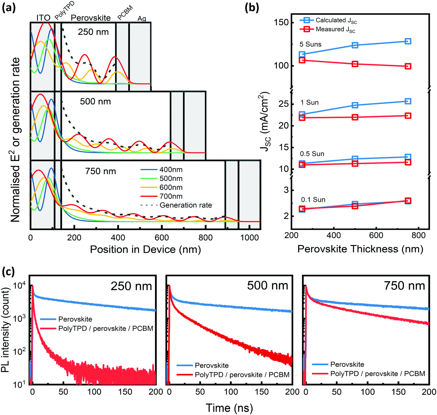 | ||
| Fig. 3 Thickness limitation of photocurrent and charge extraction. (a) Distribution of normalized optical field intensity for four wavelengths (400, 500, 600 and 700 nm), and the normalized charge generation rate in the solar cells. (b) Dependence of calculated JSC and measured JSC on perovskite thickness under four representative light intensities. (c) Time-resolved PL decay data for perovskite films and PolyTPD/perovskite/PCBM stacks, with perovskite layer thicknesses of 250 nm (left), 500 nm (middle) and 750 nm (right). The excitation density is 0.24 μJ cm−2. | ||
The limitation of charge extraction efficiency by increase of thickness can be further elucidated by time-resolved photoluminescence (PL) spectroscopy, Fig. 3c and d. The PL decays of both neat perovskite films can be fitted to a bi-exponential decay, with the faster phase assigned primarily to charge trapping and the slower phase to bimolecular recombination, as reported previously.46 While the decay dynamics of neat films show no noticeable changes, suggesting consistency of bulk film properties, a clear difference is shown when charge transport layers are added: in presence of HTL and ETL the PL decay is greatly accelerated for the 250 nm film, assigned to electron transfer to PCBM and hole transfer to PolyTPD, while for the 750 nm film the change of decay dynamics is rather small indicating slow charge transport to the contact layers, suggesting increased charge transport time to the contact layers as film thickness increases, consistent with a previous report that charge transport time should be governed by film thickness.47 Such a slowdown in charge transport is particularly detrimental to efficient charge extraction at higher light intensities, shown in previous studies,21 where the increased photo-generation yield and thus faster overall bimolecular recombination rate results in more severe recombination losses competing with charge extraction from the device.
Analyses of charge extraction versus recombination
The competition between charge extraction versus bimolecular recombination in PSC can be probed by measuring the steady-state photoluminescence (PL) from complete solar cells at open circuit (OC) and at short circuit (SC).32 PL from PSCs derives primarily from the radiative component of bulk bimolecular recombination, with variations in the intensity of PL primarily resulting from variations in the rates of non-radiative processes (e.g. charge extraction or trapping). As such, an efficient PSC should have weak PL emission at SC (PLSC) due to efficient charge extraction but maximal PL emission at OC (PLOC) due to the maximal quasi-Fermi level splitting resulting charge accumulation in the photoactive layer.32,48 In Fig. 4 the PL spectra at OC and SC are shown with excitation intensity equivalent to 0.2 sun and 6 suns, from which we define an OC-to-SC quenching efficiency (PLQOC–SC) as a calculation of (PLOC–PLSC)/PLOC, Table 2, describing the magnitude of the difference in PL emission intensity between OC and SC.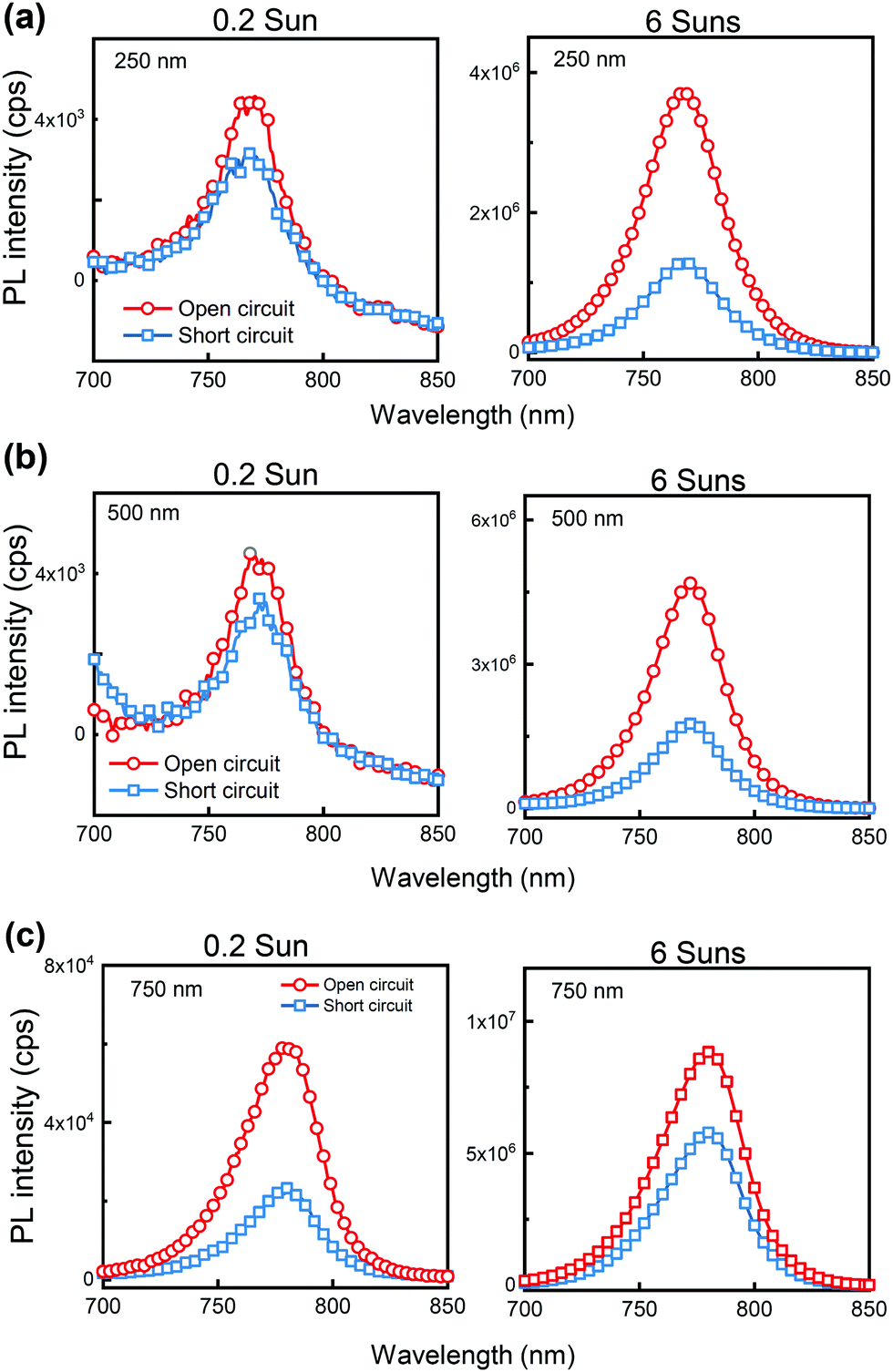 | ||
| Fig. 4 Impact of thickness on charge extraction versus recombination. PL spectra of complete device at open circuit and short circuit with (a) 250 nm, (b) 500 nm and (c) 750 nm perovskite films, excited with 635 nm continuous-wave laser with excitation density equivalent to 0.2 sun and 6 suns. | ||
| Perovskite thickness (nm) | PLQOC–SC/% | |
|---|---|---|
| 0.2 sun | 6 suns | |
| 250 | 27 | 66 |
| 500 | 28 | 62 |
| 750 | 62 | 35 |
It is clear from Table 2 that, under both light intensities, a higher PLQOC–SC is correlated with higher PCE, as expected from the general photovoltaic physics.32,49 Due to negligible charge extraction loss for all devices under 0.2 sun (see from Fig. 3b that calculated JSC's match well with measured JSC's under low light intensities), we would expect PLSC to be intrinsically low, thus the higher of PLQOC–SC for the 750 nm device under 0.2 sun is mainly a result of enhanced PLOC, indicating suppression of non-radiative recombination at open circuit for these thicker devices, consistent with their higher VOC. This is in-line with recent studies in which higher VOC was correlated with higher PL emission or longer PL lifetimes at open circuit.50,51 The trend is reversed under 6 suns where bimolecular recombination starts to dominate, that the 750 nm device exhibits a lower PLQOC–SC, resulting from considerably intensified PLSC. This is indicative of higher bimolecular recombination losses in the perovskite layer during charge extraction, correlated with the reduced JSC and FF for this thicker device under these high light intensities. This is also analogous to the observation that poor PL quenching between maximum power point and open circuit correlates with lower FF, both suggesting PL quenching is an effective assay of efficient charge extraction.48
Origin of VOC improvements
Finally we turn to more quantitative consideration of why VOC increases with perovskite film thickness, in particular how perovskite thickness impacts upon the distribution of photogenerated charge carriers at open circuit.52,53Fig. 5a shows the stabilized VOC as a function of light intensity; it is apparent that the VOC of thinner devices exhibits a steeper voltage increase with increasing light intensity, resulting in larger VOC differences between the thick and thin devices at lower light levels.54 Employing the differential charging technique, we measured the device differential capacitance (Fig. S8, ESI†) and integrated these to calculate the charge density stored in the device at open circuit under varying light intensities.55,56Fig. 5b displays the charge density per unit area n [cm−2] from approximately 0.1 sun to 3 suns. The 750 nm device shows an exponential increase of n with light intensity, typical of charge accumulation in an exponential distribution of tail states in the bulk of the perovskite layer.56 In contrast, the 250 nm device exhibits an enhanced charge density in the low light region, corresponding to a constant capacitance indicative of charge accumulation on device contacts. Although determination of the volume density of charge carriers [cm−3] remains challenging if their detailed spatial distribution in the device is unknown, such observations indicate the fraction of total charges that resides on or near the contact layers is considerable higher in 250 nm device than in 750 nm device, particularly at low light levels.19,52,56,57 | ||
| Fig. 5 Origin of VOC improvement in thick PSC. (a) Stabilized VOC as a function of light intensity, plot with the reconstructed VOC. (b) Charge carrier density per unit area [cm−2] as a function of VOC. (c) The lifetime of charge carrier as a function of VOC derived from transient photovoltage measurement. | ||
Charge carrier recombination kinetics at VOC can be determined from small-perturbation lifetimes obtained from fitting the transient photovoltage (TPV) transients with single exponential. The TPV lifetime (τΔn), Fig. 5c, decreases exponentially with VOC for both devices, while the thinner device shows moderately shorter lifetime at a given VOC and exhibits a steeper drop as VOC is increased. Fitting n–VOC and τΔn–VOC data (Fig. S9 and S10, ESI†), we can derive a reaction order δ that allows the small-perturbation lifetime to be convert to the lifetime τn of total charge, where these measured n and τn were used to calculate a predicted VOCversus light intensity, employing JSC as a measure of the density of charge photogeneration (Fig. S11, ESI†). This predicted VOC which was found to be in good agreement with measured VOCversus light intensity, as plotted in Fig. 5a, confirming that these analyses correctly determine the charge accumulation and recombination processes determining VOC.
These transient analyses confirm that decreasing of perovskite thickness results in a greater fraction of charge residing in the contact layers (charge transport layers + electrodes) instead of in the bulk of perovskite layer. As report previously,56 charge accumulation on the contact layers is most dominant at low light levels, as this charge density approximately increases linearly with device VOC, whereas bulk charge density increases exponentially. Then the reduction of VOC in the thin device can be understood as primarily resulting from enhanced charge recombination losses at the device contacts.
Discussion and conclusions
The above results show that the photoactive layer thickness of p–i–n planar perovskite solar cells for optimum photovoltaic PCE depends upon the incident light intensity, and that this behaviour depends in particular upon the light intensity dependence of the kinetic competition between charge extraction and bulk recombination. These findings are schematically illustrated by the flat-band energy diagram in Fig. 6: a thicker perovskite layer absorbs more light that can be converted into additional photocurrent under weak-light conditions where the bimolecular recombination losses at short circuit are small, in addition that reduced charge density at the interfaces suppresses interfacial recombination and yields higher VOC and FF. These factors combine to yield significantly enhanced weak-light PCEs for thicker perovskite layers (Fig. 6a). The performance of thinner devices under low light intensities are limited by a decrease of photo-absorption and are further reduced by greater interfacial recombination owing to greater proportion of charge accumulation on the contact layers (Fig. 6b). However, as the charge transport time to the charge collection layers is mainly governed by film thickness, independent of light intensity, the acceleration of bimolecular recombination with increasing light intensity becomes the key determinant of device high-light performance. Thus, thicker devices exhibit much greater charge extraction losses as the light intensity is increased (Fig. 6c), resulting in a considerable reduction of PCE. In contrast the thinner devices yield the highest PCE's at high light levels due to more efficient charge extraction (Fig. 6d). | ||
| Fig. 6 Light-intensity and thickness dependent working principles of PSC. Schematic drawing of flat-band energy diagram of p–i–n PSCs with thin and thick perovskite films under (a and b) low light condition, and (c and d) high light conditions. | ||
Our results provide key guidance to the design of PSCs for different real-world applications. They show that fabrication of relatively thick perovskite layer can considerably improve the average PCE throughout the day under normal operational conditions, particularly in northern latitudes or more shaded sites where light intensities are often less than AM 1.5, given that film quality is not sacrificed due to thickness increase. Such thicker devices will also yield higher performance for indoor light harvesting applications.30 On the contrary, for concentrator photovoltaics where high irradiance is implemented to achieve higher power output per unit area, a PSC with relatively thin perovskite layer would yield higher PCEs.
Conflicts of interest
There are no conflicts to declare.Acknowledgements
The authors acknowledge funding from Stephen and Ana Hui Fellowship (Imperial College London) and China Scholarship Council. This work was supported by the Global Research Laboratory Program of the National Research Foundation (NRF) funded by the Ministry of Science, ICT & Future Planning (NRF-2017K1A1A2013153); the GIST-ICL International Collaboration R&D Centre and EPSRC GCRF project SUNRISE (EP/P032591/1). Additionally, we acknowledge the EPSRC Centre for Doctoral Training in Plastic Electronic Materials EP/L016702/1 for continued student support and training.References
- Best Research-Cell Efficiencies Rev. 01-03-2019 (NREL, 2019); https://www.nrel.gov/pv/assets/pdfs/pv-efficiency-chart.20190103.
- K. Domanski, E. A. Alharbi, A. Hagfeldt, M. Grätzel and W. Tress, Nat. Energy, 2018, 3, 61–67 CrossRef CAS.
- H. J. Snaith, Nat. Mater., 2018, 17, 372–376 CrossRef CAS PubMed.
- T. Du, C. H. Burgess, C.-T. Lin, F. Eisner, J. Kim, S. Xu, H. Kang, J. R. Durrant and M. A. McLachlan, Adv. Funct. Mater., 2018, 28, 1803943 CrossRef.
- P. Lopez-Varo, J. A. Jiménez-Tejada, M. García-Rosell, S. Ravishankar, G. Garcia-Belmonte, J. Bisquert and O. Almora, Adv. Energy Mater., 2018, 8, 1702772 CrossRef.
- W. Tress, K. Domanski, B. Carlsen, A. Agarwalla, E. A. Alharbi, M. Graetzel and A. Hagfeldt, Nat. Energy, 2019, 4, 568–574 CrossRef CAS.
- T. Kirchartz, T. Agostinelli, M. Campoy-Quiles, W. Gong and J. Nelson, J. Phys. Chem. Lett., 2012, 3, 3470–3475 CrossRef CAS PubMed.
- D. Bartesaghi, I. D. C. Pérez, J. Kniepert, S. Roland, M. Turbiez, D. Neher and L. J. A. Koster, Nat. Commun., 2015, 6, 2–11 Search PubMed.
- Q. Zhang, B. Kan, X. Wan, H. Zhang, F. Liu, M. Li, X. Yang, Y. Wang, W. Ni, T. P. Russell, Y. Shen and Y. Chen, J. Mater. Chem. A, 2015, 3, 22274–22279 RSC.
- F. Liu, J. Zhu, J. Wei, Y. Li, M. Lv, S. Yang, B. Zhang, J. Yao and S. Dai, Appl. Phys. Lett., 2014, 104, 1–5 Search PubMed.
- G. W. P. Adhyaksa, E. Johlin and E. C. Garnett, Nano Lett., 2017, 17, 5206–5212 CrossRef CAS PubMed.
- W. E. I. Sha, X. Ren, L. Chen, W. C. H. Choy, W. E. I. Sha, X. Ren, L. Chen and W. C. H. Choy, Appl. Phys. Lett., 2015, 106, 221104 CrossRef.
- N. J. Jeon, J. H. Noh, Y. C. Kim, W. S. Yang, S. Ryu and S. Il Seok, Nat. Mater., 2014, 13, 897–903 CrossRef CAS PubMed.
- Q. Lin, A. Armin, R. Chandra, R. Nagiri, P. L. Burn and P. Meredith, Nat. Photonics, 2014, 9, 106–112 CrossRef.
- H. Zhou, Q. Chen, G. Li, S. Luo, T. Song, H.-S. Duan, Z. Hong, J. You, Y. Liu and Y. Yang, Science, 2014, 345, 542–546 CrossRef CAS PubMed.
- Z. Liu, L. Qiu, E. J. Juarez-Perez, Z. Hawash, T. Kim, Y. Jiang, Z. Wu, S. R. Raga, L. K. Ono, S. F. Liu and Y. Qi, Nat. Commun., 2018, 9, 3880 CrossRef PubMed.
- J. Chen, L. Zuo, Y. Zhang, X. Lian, W. Fu, J. Yan, J. Li, G. Wu, C. Z. Li and H. Chen, Adv. Energy Mater., 2018, 8, 1–10 Search PubMed.
- J. P. Correa-Baena, M. Anaya, G. Lozano, W. Tress, K. Domanski, M. Saliba, T. Matsui, T. J. Jacobsson, M. E. Calvo, A. Abate, M. Grätzel, H. Míguez and A. Hagfeldt, Adv. Mater., 2016, 1, 5031–5037 CrossRef PubMed.
- D. Kiermasch, L. Gil-Escrig, A. Baumann, H. J. Bolink, V. Dyakonov and K. Tvingstedt, J. Mater. Chem. A, 2019, 7, 14712–14722 RSC.
- D. W. deQuilettes, K. Frohna, D. Emin, T. Kirchartz, V. Bulovic, D. S. Ginger and S. D. Stranks, Chem. Rev., 2019, 119, 11007–11019 CrossRef CAS PubMed.
- E. M. Hutter, J. J. Hofman, M. L. Petrus, M. Moes, R. D. Abellón, P. Docampo and T. J. Savenije, Adv. Energy Mater., 2017, 7, 1–8 Search PubMed.
- C. L. Davies, M. R. Filip, J. B. Patel, T. W. Crothers, C. Verdi, A. D. Wright, R. L. Milot, F. Giustino, M. B. Johnston and L. M. Herz, Nat. Commun., 2018, 9, 293 CrossRef PubMed.
- P. W. Stackhouse, T. Zhang, D. Westberg, A. J. Barnett, T. Bristow, B. Macpherson, J. M. Hoell and B. A. Hamilton, POWER Release 8.0.1 (with GIS Applications) Methodology, NASA Langley Research Center, 1, 2018 Search PubMed.
- V. Stoichkov, N. Bristow, J. Troughton, F. De Rossi, T. M. Watson and J. Kettle, Sol. Energy, 2018, 170, 549–556 CrossRef CAS.
- Y. Reyna, M. Salado, S. Kazim, A. Pérez-Tomas, S. Ahmad and M. Lira-Cantu, Nano Energy, 2016, 30, 570–579 CrossRef CAS.
- Z. Wang, Q. Lin, B. Wenger, M. G. Christoforo, Y. H. Lin, M. T. Klug, M. B. Johnston, L. M. Herz and H. J. Snaith, Nat. Energy, 2018, 3, 855–861 CrossRef CAS.
- E. Cuce, P. M. Cuce and T. Bali, Appl. Energy, 2013, 111, 374–382 CrossRef CAS.
- N. H. Reich, W. Van Sark, E. A. Alsema, S. Y. Kan, S. Silvester, A. Van Der Heide, R. W. Lof and R. Schropp, 20th Eur. Photovolt. Sol. Energy Conf., 2005, pp. 4–7.
- H. K. H. Lee, J. Wu, J. Barbé, S. M. Jain, S. Wood, E. M. Speller, Z. Li, F. A. Castro, J. R. Durrant and W. C. Tsoi, J. Mater. Chem. A, 2018, 6, 5618–5626 RSC.
- H. K. H. Lee, J. Barbé, S. M. P. Meroni, T. Du, C. Lin, A. Pockett, J. Troughton, S. M. Jain, F. De Rossi and J. Baker, Sol. RRL, 2019, 3, 1800207 CrossRef.
- T. Liu, K. Chen, Q. Hu, R. Zhu and Q. Gong, Adv. Energy Mater., 2016, 6, 1600457 CrossRef.
- T. Du, W. Xu, M. Daboczi, J. Kim, S. Xu, C.-T. Lin, H. Kang, K. Lee, M. J. Heeney, J.-S. Kim, J. R. Durrant and M. A. McLachlan, J. Mater. Chem. A, 2019, 7, 18971–18979 RSC.
- N. Wijeyasinghe, A. Regoutz, F. Eisner, T. Du, L. Tsetseris, Y.-H. Lin, H. Faber, P. Pattanasattayavong, J. Li, F. Yan, M. A. McLachlan, D. J. Payne, M. Heeney and T. D. Anthopoulos, Adv. Funct. Mater., 2017, 27, 1701818 CrossRef.
- D. Zhao, C. Chen, C. Wang, M. M. Junda, Z. Song, C. R. Grice, Y. Yu, C. Li, B. Subedi, N. J. Podraza, X. Zhao, G. Fang, R.-G. Xiong, K. Zhu and Y. Yan, Nat. Energy, 2018, 3, 1093–1100 CrossRef CAS.
- J. Lee, H. Kang, G. Kim, H. Back, J. Kim, S. Hong, B. Park, E. Lee and K. Lee, Adv. Mater., 2017, 29, 1–8 Search PubMed.
- J. M. Ball, S. D. Stranks, M. T. Hörantner, S. Hüttner, W. Zhang, E. J. W. Crossland, I. Ramirez, M. Riede, M. B. Johnston, R. H. Friend and H. J. Snaith, Energy Environ. Sci., 2015, 8, 602–609 RSC.
- G. Zhang, K. Zhang, Q. Yin, X. F. Jiang, Z. Wang, J. Xin, W. Ma, H. Yan, F. Huang and Y. Cao, J. Am. Chem. Soc., 2017, 139, 2387–2395 CrossRef CAS PubMed.
- F. De Rossi, J. A. Baker, D. Beynon, K. E. A. Hooper, S. M. P. Meroni, D. Williams, Z. Wei, A. Yasin, C. Charbonneau, E. H. Jewell and T. M. Watson, Adv. Mater. Technol., 2018, 3, 1–9 Search PubMed.
- S. Meloni, T. Moehl, W. Tress, M. Franckevičius, M. Saliba, Y. H. Lee, P. Gao, M. K. Nazeeruddin, S. M. Zakeeruddin, U. Rothlisberger and M. Graetzel, Nat. Commun., 2016, 7, 10334 CrossRef CAS PubMed.
- S. Van Reenen, M. Kemerink and H. J. Snaith, J. Phys. Chem. Lett., 2015, 6, 3808–3814 CrossRef CAS PubMed.
- T. Du, C. H. Burgess, J. Kim, J. Zhang, J. R. Durrant and M. A. McLachlan, Sustainable Energy Fuels, 2017, 1, 119–126 RSC.
- G. F. Burkhard, E. T. Hoke and M. D. McGehee, Adv. Mater., 2010, 22, 3293–3297 CrossRef CAS PubMed.
- S. Haque, M. J. Mendes, O. Sanchez-Sobrado, H. Águas, E. Fortunato and R. Martins, Nano Energy, 2019, 59, 91–101 CrossRef CAS.
- S. Haque, M. Alexandre, M. J. Mendes, H. Águas, E. Fortunato and R. Martins, Appl. Mater. Today, 2020, 20, 100720 CrossRef.
- Q. Lin, Z. Wang, H. J. Snaith, M. B. Johnston and L. M. Herz, Adv. Sci., 2018, 5, 1–8 Search PubMed.
- J. Kim, R. Godin, S. D. Dimitrov, T. Du, D. Bryant, M. A. McLachlan and J. R. Durrant, Adv. Energy Mater., 2018, 8, 1802474 CrossRef.
- G. Xing, N. Mathews, S. Sun, S. S. Lim, Y. M. Lam, M. Grätzel, S. Mhaisalkar and T. C. Sum, Science, 2013, 342, 344–347 CrossRef CAS PubMed.
- M. Stolterfoht, V. M. Le Corre, M. Feuerstein, P. Caprioglio, L. J. A. Koster and D. Neher, ACS Energy Lett., 2019, 4, 2887–2892 CrossRef CAS.
- K. Tvingstedt, O. Malinkiewicz, A. Baumann, C. Deibel, H. J. Snaith, V. Dyakonov and H. J. Bolink, Sci. Rep., 2014, 4, 1–7 Search PubMed.
- M. Stolterfoht, C. M. Wolff, J. A. Márquez, S. Zhang, C. J. Hages, D. Rothhardt, S. Albrecht, P. L. Burn, P. Meredith, T. Unold and D. Neher, Nat. Energy, 2018, 3, 847–854 CrossRef CAS.
- Z. Liu, L. Krückemeier, B. Krogmeier, B. Klingebiel, J. A. Márquez, S. Levcenko, S. Öz, S. Mathur, U. Rau, T. Unold and T. Kirchartz, ACS Energy Lett., 2019, 4, 110–117 CrossRef CAS.
- F. Deledalle, P. Shakya Tuladhar, J. Nelson, J. R. Durrant and T. Kirchartz, J. Phys. Chem. C, 2014, 118, 8837–8842 CrossRef CAS.
- I. Gelmetti, L. Cabau, N. F. Montcada and E. Palomares, ACS Appl. Mater. Interfaces, 2017, 9, 21599–21605 CrossRef CAS PubMed.
- W. Tress, M. Yavari, K. Domanski, P. K. Yadav, B. Niesen, J.-P. Correa-Baena, A. Hagfeldt and M. Grätzel, Energy Environ. Sci., 2018, 11, 151–165 RSC.
- T. Du, J. Kim, J. Ngiam, S. Xu, P. R. F. Barnes, J. R. Durrant and M. A. McLachlan, Adv. Funct. Mater., 2018, 28, 1801808 CrossRef.
- S. Wheeler, D. Bryant, J. Troughton, T. Kirchartz, T. M. Watson, J. Nelson and J. R. Durrant, J. Phys. Chem. C, 2017, 121, 13496–13506 CrossRef CAS.
- T. Kirchartz and J. Nelson, Phys. Rev. B: Condens. Matter Mater. Phys., 2012, 86, 1–12 CrossRef.
Footnote |
| † Electronic supplementary information (ESI) available. See DOI: 10.1039/d0tc03390a |
| This journal is © The Royal Society of Chemistry 2020 |