
 Open Access Article
 This Open Access Article is licensed under a Creative Commons Attribution-Non Commercial 3.0 Unported Licence
Unravelling the effect of fluorinated ligands in hybrid EUV photoresists by X-ray spectroscopy†
Lianjia
Wu
 a,
Ivan
Bespalov
a,
Katharina
Witte
b,
Olivier
Lugier
a,
Jarich
Haitjema
a,
Michaela
Vockenhuber
b,
Yasin
Ekinci
b,
Benjamin
Watts
b,
Albert M.
Brouwer
ac and
Sonia
Castellanos
*a
a,
Ivan
Bespalov
a,
Katharina
Witte
b,
Olivier
Lugier
a,
Jarich
Haitjema
a,
Michaela
Vockenhuber
b,
Yasin
Ekinci
b,
Benjamin
Watts
b,
Albert M.
Brouwer
ac and
Sonia
Castellanos
*a
aAdvanced Research Center for Nanolithography, Science Park 106, 1098 XG Amsterdam, The Netherlands. E-mail: s.castellanos@arcnl.nl
bPaul Scherrer Institute, Forschungstrasse 111, Villigen 5232, Switzerland
cvan’t Hoff Institute for Molecular Sciences, University of Amsterdam, P.O. Box 94157, 1090 GD Amsterdam, The Netherlands
First published on 13th October 2020
Abstract
Organic–inorganic hybrid compounds are arising as promising resist materials for extreme-ultraviolet (EUV) lithography, a new technique introduced in the semiconductor industry for the fabrication of integrated circuits of sub-10 nm feature size. In this work, we show that the sensitivity to EUV radiation of zirconium oxo clusters with methacrylate ligands is substantially enhanced when a small fraction of the ligands are replaced by trifluoromethylacrylates. We studied the details of the chemical changes that occur in thin films of the precursor and the partially fluorinated materials using scanning transmission X-ray microscopy (STXM) and X-ray photoelectron spectroscopy (XPS). Evidence is presented for radical chain polymerization as a mechanism for the solubility switch. Yet, XPS results also indicate that Zr–F bonds are formed during the exposure to EUV light in the fluorinated material, dissociative electron attachment being likely involved. Our observations show that, while fluorinated ligands enhance EUV absorption, their effect on the reactivity of the material might be more critical, thereby contributing to an increase in the sensitivity of the resist in both ways.
Introduction
EUV lithography is a cutting-edge technology that can enable the fabrication of integrated circuits for computer chips and memory devices with feature sizes below 10 nm.1,2 Thanks to the employment of shorter wavelength (13.5 nm) than in previous lithographic techniques (193 nm), EUV lithography can yield a higher resolution. Yet, a challenge remains; to find photoresist materials that can efficiently absorb the EUV photons from the optical projection and transform them into high-quality nanopatterns after development.3–5Although photoresists based on polymeric platforms have been used in optical lithography until now, these materials are not optimal for EUV lithography for several reasons,6 one of the most important being their low EUV absorptivity.5,7 Therefore, finding new resists that fulfil the requirements for the fabrication of the next generation of integrated circuits is of paramount importance. EUV resists should be able to print high-quality patterns with feature sizes below 20 nm at cost-effective exposure times, that is, using low EUV doses (ideally < 20 mJ cm−2).8,9 Further, a low defect density in the patterns is required, an aspect that has been correlated to the EUV absorptivity of the resist. That is, high absorptivity reduces some type of defects in the final pattern.10,11 Heterogeneities in the composition of the resist film are also considered a source of defects,12,13 since they contribute to the stochastic distribution of chemical reactions around the photon absorption area.
Molecular materials that incorporate metals in their structures—typically known as inorganic resists—are gaining interest5,14,15 since they offer higher EUV absorption cross-sections and have yielded better nanopatterning performance compared to polymer-based ones.6,8,9 Yet, what makes the design of a novel EUV resist challenging is that the chemistry induced by EUV photons is not well understood.16 EUV photons, with an energy of 92 eV, do not initiate “classical” photochemistry, but rather eject electrons from the valence band or, when applicable, from some inner core orbitals to the continuum, leading to the ionization of the molecule. The ejected photoelectron has an excess of kinetic energy that is transferred to the surroundings through inelastic scattering events. During the scattering, more molecules can be ionized so that secondary electrons are generated, which have a broad distribution of kinetic energies in the 0–80 eV range.14 Therefore, the chemistry induced by EUV photons is the result of the electron-induced chemistry17–19 and the chemical processes that the ionized molecules undergo. Furthermore, the probability of absorbing EUV photons by molecules is mainly determined by their elemental composition rather than by the selection rules based on the characteristics of the frontier molecular orbitals that apply in photochemistry.7,20
Metal oxoclusters (MOCs) are promising materials for the next generation of inorganic EUV resists. First, they comprise metals, which can significantly enhance the EUV absorptivity of the material, as explained above. Second, they are molecularly defined, meaning that they consist of molecular units of small size and thus offer homogeneity in their composition. Both characteristics are expected to benefit the lithographic performance in terms of roughness and defect density in the patterns.12,13,21 And, third, in the case of MOCs comprising carboxylate ligands, the composition of their organic shell can be easily modified by means of ligand exchange reactions. This provides a quite straightforward manner of changing the properties of the layer (e.g., density and processability) and its reactivity towards EUV light with small synthetic effort.22–24
The EUV printability of metal-containing molecular photoresists has been demonstrated on metal oxo clusters based on Zr, Hf, Zn, and Sn21,24–29 and metal complexes based on Sb, Bi, Sn, and Te.30,31 Investigations were devoted to broadening the range of metal centers,21,31–33 as they are important for EUV absorptivity of the material. Several examples show the influence of different functional ligands on the photoresist performance of metal oxo clusters,34 metal complexes,30,35 and metal oxide nanoparticles,36 but the patterning mechanisms remain to be elucidated. Only a few studies provide spectroscopic insights into the EUV-induced chemistries of the ligands in those hybrid molecular photoresists.25,26,29,37
In this work, we introduce a small fraction of fluorinated methacrylate ligands in Zr-based resists that originally have an organic shell composed of solely methacrylate ligands. The incorporation of the fluorine species aimed at increasing the EUV absorptivity (and, in consequence, the sensitivity) of the material. As shown below, the “doping” of the organic shell23 substantially enhances the material's sensitivity in EUV lithography. The chemical changes resulting from EUV exposure in both materials were monitored by means of scanning transmission soft X-ray microscopy (STXM) and X-ray photoelectron spectroscopy (XPS). These techniques are especially convenient to study EUV resists, since they can be applied on very thin films (∼30 nm thick) and give very specific information about changes in chemical bonding, i.e., they can be used to elucidate what type of reactions occur in the thin film. It was found that, in addition to the cross-linking reactions between methacrylate ligands happening in both clusters, the presence of fluorinated ligands opened a new reaction path where C–F bonds are dissociated, thus making the fluorinated material more reactive towards EUV photons.
Results and discussion
Recently, the Zr-oxocluster comprising methacrylate ligands in the organic shell, Zr6O4(OH)4Mc12, abbreviated as ZrMc, was proven to act as a negative tone EUV resist.26 The material rendered a relatively good sensitivity in terms of the minimum dose necessary to change the solubility in the solvent used to deposit thin films of the pristine material (D0). This dose is measured by means of contrast curves, an experiment in which the thickness of exposed resist remaining after development (for a fixed time) is measured for varying exposure doses. This gives evidence of changes in the solubility rate and, therefore, proof of chemical changes after exposure.38 Despite the good sensitivity of the material, its linear absorbance at 92 eV is rather low (calculated 4.2 μm−1, experimental 5 μm−1).20Aiming at enhancement in the EUV absorptivity of the material, a fluorinated version of the methacrylate ligand was introduced in the organic shell. Metal oxoclusters comprising carboxylate ligands undergo ligand exchange reactions with ligands that feature the same chelating groups. This allows for the easy modification of the composition of their organic shell.22–24,39,40 The incorporation of the fluorinated ligand was thus performed by means of ligand exchange reaction using a low ratio of fluorinated methacrylate ligands, TFMc, in relation to the methacrylate ligand, Mc, present in the original cluster (an average of 1 TFMc over 12 ligands). That is, we doped ZrMc with TFMc ligands to yield a mixture of clusters with an average molecular formula Zr6O4(OH)4Mc11TFMc, here ZrMcF (Scheme 1). By doping the organic shell most of the physicochemical properties of the material, such as its processability in solvents, are preserved while the specific effect of the doping ligand in the lithographic performance can be tracked down. It should be noticed that the incorporation of the fluorinated ligand in the molecular structure even in such a small ratio can increase the linear EUV absorptivity of the resist by 10%.34
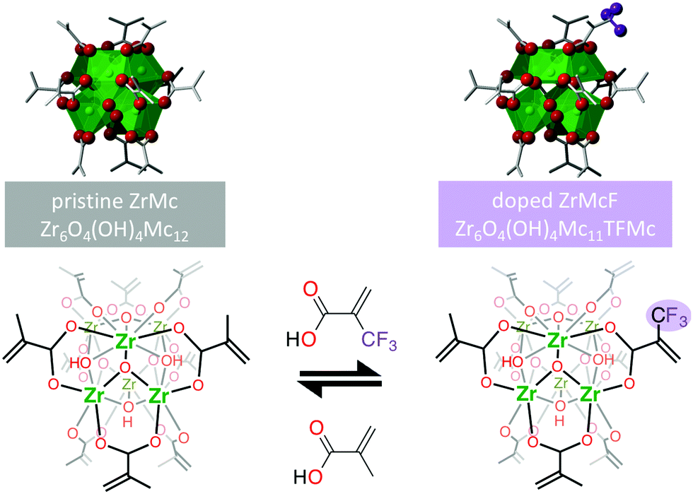 | ||
| Scheme 1 Ligand exchange reaction on ZrMc to synthesize the doped ZrMcF. On top, 3D representations of the cluster made from the crystal X-ray diffraction data of the pristine ZrMc:41 green octahedra represent the coordination geometry of Zr4+ cations, red spheres represent oxygen atoms, grey bars represent the carbon backbone of the ligands. Fluorine atoms were added for representation purposes. Protons in μ3-bridging OH groups of the oxo-cluster are omitted for simplicity. | ||
The pristine ZrMc and the doped ZrMcF compounds were deposited by means of spin-coating on silicon substrates. The thin films were exposed to EUV (synchrotron light at 92 eV) using an open-frame mask for large areas (aperture size of 1.7 × 1.7 mm2 or 0.5 × 0.5 mm2) or by means of interference lithography (EUV-IL)2,42,43 to print dense line/space patterns. The exposed thin films of both materials were subsequently developed using the same conditions (developer and development time). The contrast curves of the two resists indicate that the fluorinated material renders higher sensitivity (Fig. 1) and an improvement of the printability of dense lines pattern was observed; while ZrMc could only resolve dense lines of 50 nm width using a dose of 57 mJ cm−2, ZrMcF could print 30 nm lines at 36 mJ cm−2 (Fig. S2, ESI†). It should be noticed that, the development conditions are not optimized for the doped material, as our main goal was to compare both resists.
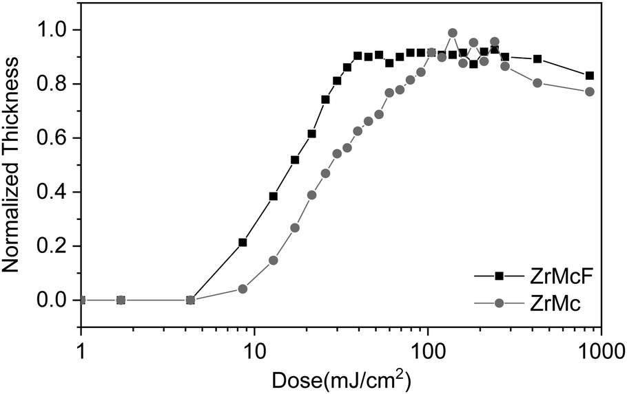 | ||
| Fig. 1 Contrast curves obtained for ZrMc and ZrMcF after exposure to EUV using an open-frame mask. | ||
Previous works have proposed that metal oxoclusters based on Zr and Hf and comprising methacrylate ligands undergo cross-linking between the double bonds of neighboring molecules upon EUV exposure.26,37 This reaction is probably initiated by radicals that are generated after ionization. Here, NEXAFS spectroscopy was used to monitor the cross-linking reaction in both EUV resists. This technique is element-specific and gives information of the chemical bonding of the studied element since resonant transitions from the core atomic orbitals to empty molecular orbitals are selectively promoted.
In particular, NEXAFS spectroscopy was performed using scanning transmission soft X-ray microscopy (STXM).44,45 This technique enables recording X-ray absorption in the soft X-ray regime with a spatial resolution of down to 20 nm. The combination of EUV exposure and ex situ STXM analysis is thus a powerful way to investigate the chemical changes undergone by the resists upon EUV exposure. This is because different doses of EUV can be applied in different regions of the same sample, and changes in the X-ray absorption can then be mapped and correlated to each EUV dose. In particular, the soft X-ray energy range promotes electronic transitions from the carbon K-edge (1s orbital), which directly corresponds to the detection of changes in the carbon backbone of the organic ligands.46–48
C K-edge NEXAFS spectroscopy was performed for the two materials, ZrMc and fluorine-doped ZrMcF. For each compound, a spectrum of the thin film before exposure to EUV light was recorded as reference (Fig. 2). The spectra of the unexposed thin films of both ZrMc and ZrMcF in Fig. 2 displayed clear, sharp peaks corresponding to electronic transitions from the C 1s orbital on the C![[double bond, length as m-dash]](https://www.rsc.org/images/entities/char_e001.gif) C terminal bond to the π* orbital of the methacrylate ligand, C 1s → π*(CC), at ∼284 eV and to the electronic transitions from the 1s orbital of the C atom on the carboxylate group to the π* orbital, C 1s → π*(CO), at ∼288 eV.46,49 The fits of the relevant peaks contributing to the NEXAFS spectra are shown in Fig. 2, and their assignments to electronic transitions are listed in Table 1.
C terminal bond to the π* orbital of the methacrylate ligand, C 1s → π*(CC), at ∼284 eV and to the electronic transitions from the 1s orbital of the C atom on the carboxylate group to the π* orbital, C 1s → π*(CO), at ∼288 eV.46,49 The fits of the relevant peaks contributing to the NEXAFS spectra are shown in Fig. 2, and their assignments to electronic transitions are listed in Table 1.
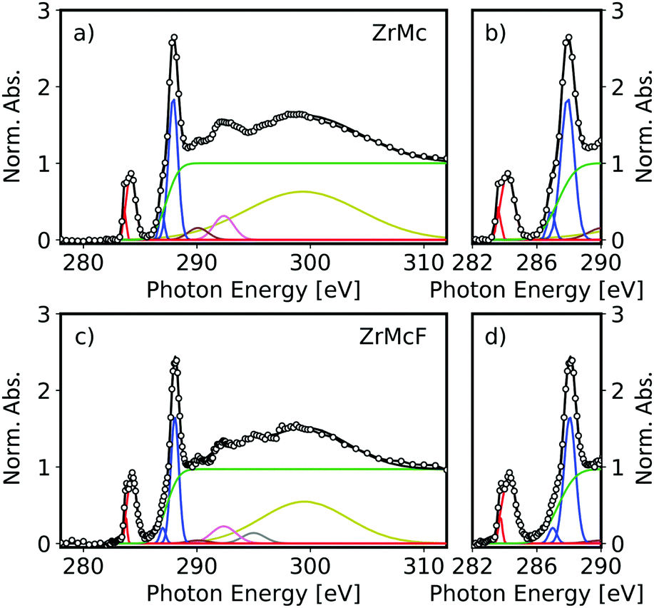 | ||
| Fig. 2 Fitted NEXAFS spectra of the C K-edge region (a) of the ZrMc resist (b) zoomed-in range and (c) of the doped ZrMcF resist (d) zoomed-in range before exposure. Gaussian peaks fit resonant transitions and the step-function (green line) fits the ionization to the continuum (edge). | ||
The fits of both the peaks assigned to C 1s → π*(CC) and the 1s → π*(CO) transitions in ZrMc and ZrMcF required at least two components each (Fig. 2). This could arise from different environments or coordination modes of the methacrylate ligands. As a matter of fact, in the crystalline form, the ZrMc cluster already presents two binding modes for the methacrylate ligands: chelating (one carboxylate group coordinates on Zr4+ cations) and bridging (one carboxylate group coordinates to two Zr4+ cations).41 In addition, we suspect that the carboxylate ligands in the cluster rearrange when they are deposited as thin films, which would also lead to different binding modes and environments around the carboxylate groups.26 However, the exact origin of the different contributions to these peaks is outside the scope of this work.
Different areas on one sample (either containing ZrMc or ZrMcF) were exposed to four different EUV doses (50, 100, 200, and 500 mJ cm−2) and each sample was developed, as represented in Fig. 3a. The spectra from the four non-dissolved features were then recorded with STXM. Fig. 3b displays the evolution of the C K-edge absorption spectra of both materials normalized to the continuum at ∼320 eV after EUV exposure. Note that the absorbance in the ionization regime is a measure of the total amount of carbon present. Therefore, this normalization allows monitoring the proportion of carbon species of interest relative to the total carbon contents. Overlapping with the C K-edge continuum, two peaks at 333.8 eV and 346.5 eV were also detected (Fig. S4, ESI†). These peaks belong to the Zr M2,3-edge, i.e. they originate from excitations of Zr 3p electrons. Although the analysis of this absorption edge is beyond the scope of the present work, we noted that the intensity of the peaks in the normalized spectra was constant over dose.
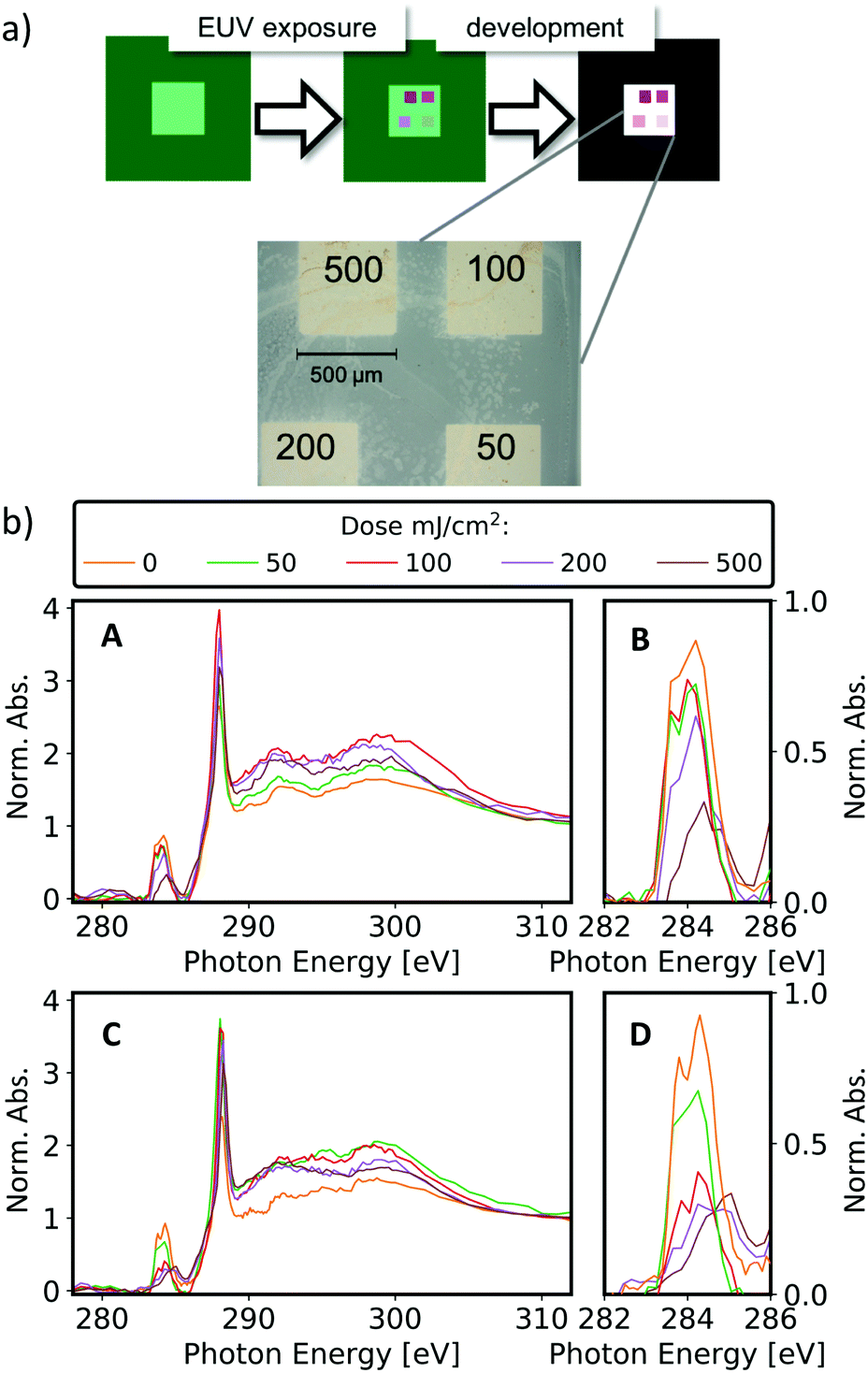 | ||
| Fig. 3 (a) Scheme showing the workflow for the experiment. The resists were spin-coated on SiNx membranes and exposed to EUV. Then, the samples were developed so that the unexposed material was selectively dissolved and the clean membrane was left between exposed areas. An optical microscope image of the sample after development is shown. EUV doses on each squared area are given in mJ cm−2. (b) NEXAFS spectra of ZrMc (A & B) and ZrMcF (C & D) before and after exposure normalized to the continuum. B and D zoom into the pre-edge region with the absorption peak assigned to C 1s → π* (CC) transition. | ||
Further trends that support chemical changes in the ligands rather than just their cleavage and loss is the evolution of the 290–310 eV region, where the C 1s → σ* (C–H/C–C) transitions occur. Although an explanation of the spectral shape evolution is non-trivial and not attempted here, we observed that the spectra of ZrMc and ZrMcF at the highest dose (500 mJ cm−2) closely resemble the C K-edge spectrum of polymethylmethacrylate (PMMA), which is the product of polymerization of methyl methacrylate (see Fig. S5 in ESI†). This resemblance is in agreement with the formation of some kind of Zr-containing hybrid polymer after ZrMc and ZrMcF are exposed to EUV light.
A clear decrease of the C 1s → π* (CC) peak with increasing EUV exposure dose is observed for both materials (Fig. 4a). Furthermore, the absorbance ratio between the peaks assigned to CC and the ones assigned to the COO (ACC/ACO in Fig. 4b) also decreases with EUV exposure. This indicates that methacrylate ligands are not just cleaved and outgassed but also the concentration of CC double bonds decreases through another process. These results are in agreement with the cross-linking mechanism proposed for the ZrMc material in previous works:26,37 Radical species resulting from ionization can lead to chain polymerization reactions among neighboring methacrylate ligands, thus decreasing the CC concentration in the material.
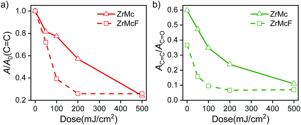 | ||
| Fig. 4 Evolution of the absorbance value (A) of some fitted peaks in normalized spectra as a function of dose. (a) Absorbance of peaks assigned to C 1s → π* (CC) (A283.6 + A284.2) relative to initial values (A/A0); (b) absorbance ratio between peaks assigned to C 1s → π* (CC) (A283.6 + A284.2) and to C 1s → π* (CO) (A286.9 + A287.9). | ||
It should be noted that a small amount of decarboxylation upon EUV exposure (<20%) was reported for ZrMc in a previous work26 based on XPS studies (see below for XPS on ZrMcF). Yet, in the NEXAFS spectra presented here, the C 1s → π* (CO) peak showed a two-step behavior with an initial intensity increase and a subsequent decrease for doses above 100 mJ cm−2 (Fig. S6, ESI†) for both materials. It should be kept in mind that the increase in the peak is relative to the continuum. So, this could indicate that other carbon species contributing to the continuum are lost while few decarboxylation events occur. In addition, the oscillator strength of the C 1s → π* (CO) peak can change depending on the functional groups that are next to the COO unit. In particular, this transition has lower intensity when π systems are conjugated to the COO group compared to aliphatic groups.53 Therefore, cross-linking reactions at lower doses might lead to an increase in the C 1s → π* (CO) peak intensity, as methacrylate ligands turn into saturated carboxylates, whereas a slight amount of decarboxylation at higher doses can lead to its decrease. It should also be noted that XPS probes only the surface of the thin film, whereas NEXAFS experiments, performed in transmission mode, probe the whole film. The fraction of COO groups that are lost in the bulk is probably below 20%.
We observed that the decrease in the CC/COO absorbance ratio was faster in the case of the F-doped material, ZrMcF, compared to the case of ZrMc (Fig. 4b), thus indicating that a larger number of reactions per incident photon occurs in the doped compound compared to the non-fluorinated ZrMc. Although ZrMcF is expected to have a slightly higher linear absorptivity, the increase is calculated as only 10% (4.2 vs. 4.6 μm−1),34 which does not explain the remarkable difference in reactivity between the two compounds (Fig. S7, ESI†). The differences in the cross-linking reaction efficiency are in line with the trends observed for the sensitivity of the two materials. As explained above, ZrMcF proved to need less EUV dose to render the whole thin film insoluble in the contrast curves.
Therefore, other processes must be inducing a higher number of cross-linking events per absorbed photon. As explained in the Introduction, the absorption of an EUV photon leads to the generation of photoelectrons of ca. 80 eV that scatter in the material and ionize other molecules. As the electrons transfer their energy, they slow down and eventually are “trapped” or recombine with an ionized molecule. The total electron yield, the reactivity of the ionized molecules, and the electron-induced reactivity can be different when the fluorine element is introduced in the material. Disentangling all these processes is a long-term goal and is out of the scope of this paper. However, the identification of different species in the thin film after exposure can give hints of reaction pathways that are enabled in the fluorinated derivative that might promote cross-linking. In addition, other reactions that contribute to the solubility switch might occur in the ZrMcF case.
To gain further insights into the role of the fluorine-containing ligand in the EUV-induced chemistry of ZrMcF, XPS was used to track changes in the resist after exposure. The experiments allowed to estimate the ratio of the different species in the pristine ZrMcF. It should be noticed that XPS is a surface technique and that these ratios might be different from those in the bulk of the sample. For instance, a partial loss of ligand is plausible on the surface but might be less favored inside the film. In addition, the accurate values of electron mean free paths for this material are not known and tabulated values given by the processing software are used, which could affect slightly the results.
Nevertheless, the most relevant results emerge from the inspection of the spectra in the F 1s region (Fig. 5a), which revealed the clear appearance of a new fluorine species upon EUV irradiation. The chemical shift for this species is typical for inorganic fluoride.54,55 This peak increases as a function of dose (empty green triangles in Fig. 5b), while, at the same time, the F 1s peak assigned to fluorine bonded to carbon originally present in the fluorinated ligand, decreases (filled green triangles in Fig. 5b). It is known that low energy electrons can easily lead to dissociation of C–F bonds.56,57 This result thus indicates that the C–F bond is dissociated, and the resulting fluoride ion is stabilized in the material, most likely through the interaction with the metal cations by forming Zr–F bonds. In fact, this particular hexanuclear Zr-clusters has shown affinity for F− ions when they are constituents (nodes) of a metal–organic framework,58 and related ZrOx particles decorated with carboxylate ligands have been used to remove F− ions from water.59
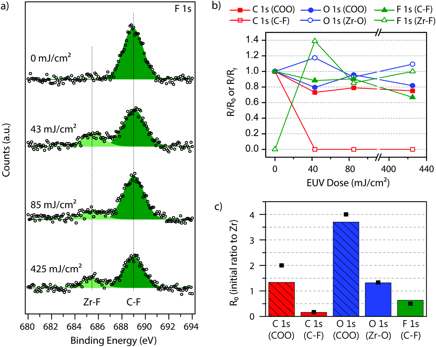 | ||
| Fig. 5 (a) High-resolution XPS of the F 1s peak of the unexposed and the exposed ZrMcF resist; experimental data plotted in circles, fitted components shown in green areas. (b) Species ratio relative to Zr (R) at each EUV dose expressed as a fraction of the initial ratio (R/R0) and, in the case of the appearing Zr–F species in F 1s, as a fraction of the final ratio (R/Rf). (c) Species ratio relative to Zr of the ZrMcF unexposed thin film (R0) calculated from the fitting of C 1s, O 1s and F 1s peaks in the X-ray photoelectron spectra (bars) and theoretical ratios calculated from the molecular formula (black squares). | ||
For O 1s and C 1s spectra the evolution of the peak profile followed the trends previously reported for ZrMc.26 The fitting of the O 1s peak (Fig. S8, ESI†) suggests a slight decrease of oxygen species from carboxylate groups (531 eV, filled blue circles in Fig. 5b) and a concomitant increase of the oxide-type species (530 eV, empty blue circles in Fig. 5b). This is in line with a small number of decarboxylation reactions followed by the oxidation/hydroxylation of the Zr-sites after EUV exposure in the presence of air, since the measurements were done ex situ. The slight loss of carboxylate groups is also in agreement with the small decrease of the peak at 289 eV (red squares in Fig. 5b) observed in the fitting of the C 1s peak in the XPS spectra (Fig. S8, ESI†). Yet, ZrMcF displayed a new peak in the C 1s spectrum at 292.4 eV compared to the spectrum of ZrMc, which is assigned to the carbon atoms participating in the C–F bond of the fluorinated ligands. Unfortunately, an accurate tracking of this peak as a function of dose is not possible due to its low intensity. Yet, the spectra indicate a decrease of this species with exposure.
Therefore, in addition to a higher degree of cross-linking per incident EUV photon, ZrMcF undergoes an extra reaction where C–F bonds are cleaved and fluoride species are formed. In fact, it is likely that such cleavage further induces polymerization reactions as it can result into the formation of transient radicals that initiate the cross-linking of the double bonds. The EUV-induced reactions for ZrMcF are shown in Scheme 2. Partial decarboxylation, ligand cross-linking and the intercalation of fluorine atoms in the resulting network lead to the solubility contrast in ZrMcF.
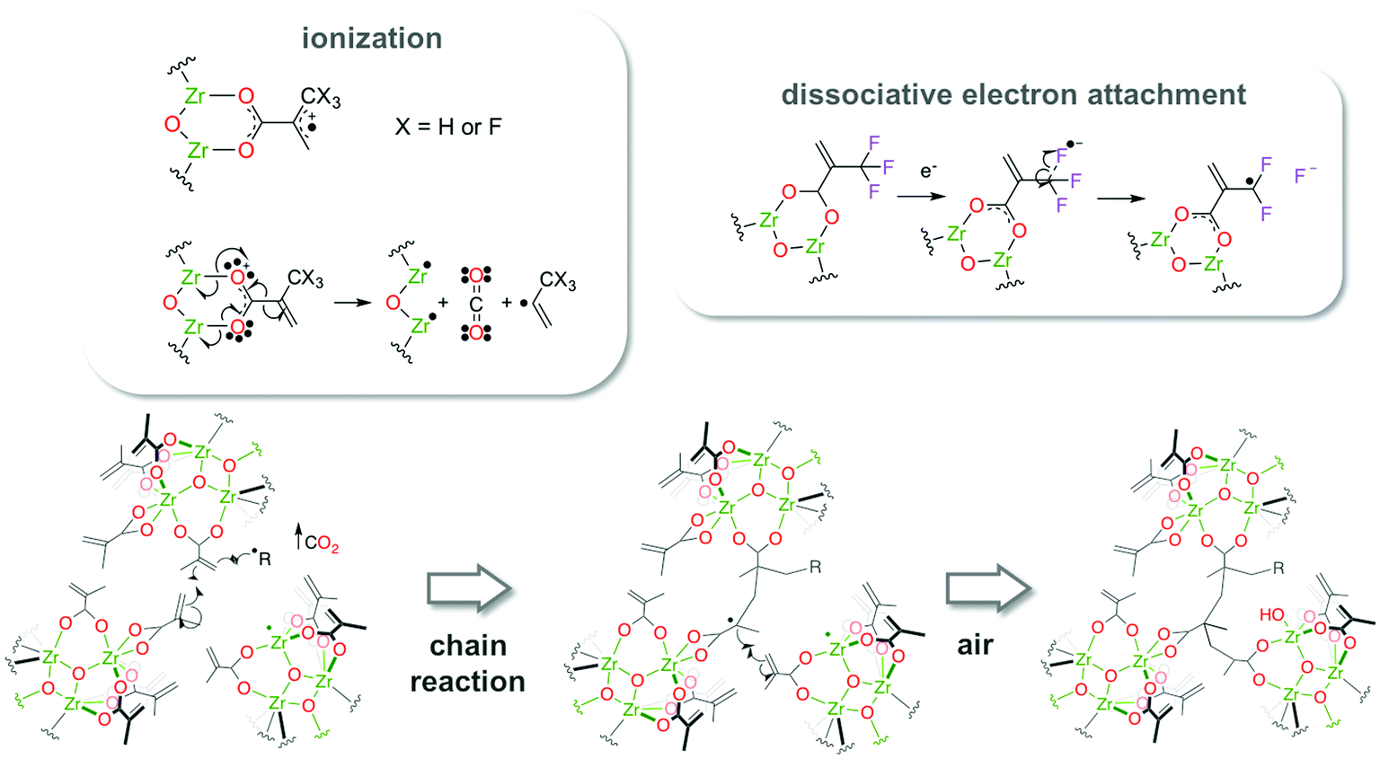 | ||
| Scheme 2 Reactions induced by EUV that lead to the formation of radicals which can initiate cross-linking of the terminal double bonds in the methacrylate ligands. | ||
Conclusions
The doping of the organic shell of a Zr-based oxocluster composed of methacrylate ligands with an analogous fluorinated ligand (trifluoromethacrylate) led to the enhancement of EUV lithographic performance. NEXAFS experiments in the C K-edge energy range revealed that the concentration of terminal double bonds in both the pristine material and the partially fluorinated analogue decreases at faster rates than the concentration of carboxylate groups upon EUV radiation. This trend is in line with a polymerization reaction involving the terminal double bonds of the methacrylate ligands, which would result in a decrease in the solubility of the clusters upon EUV exposure and would thus enable the formation of patterns with EUV lithography. The evolution of the X-ray absorption spectra with incident dose points at a more efficient reaction in the fluorine-containing material compared to the undoped one, i.e. more double bonds react for the same incident dose. Furthermore, X-ray photoelectron spectroscopy indicates that an extra reaction pathway takes place in the doped resist: the dissociation of C–F bond and formation of inorganic fluoride, presumably stabilized by the formation of Zr–F bonds. We thus attribute the better printability of the material doped with fluorinated ligands to the synergistic contribution of two factors: a slightly higher EUV absorptivity and the appearance of a new reaction pathway where C–F bonds are cleaved. The latter could be a source of radical species that further initiate the cross-linking reactions, which leads to a new product comprising fluoride ions. This work shows how a simple modification in the molecular structure of a hybrid material can result in a significant optimization of the material as an EUV resists. Mainly, the introduction of different functionalities in the organic shell of this type of materials can open new reaction channels originating from the ionization of the molecules and/or from their interaction with low energy electrons.Experimental
Thin-film deposition and EUV exposure
The pristine Zr6O4(OH)4Mc12, Mc = methacrylate, here labeled as ZrMc, was synthesized as previously reported.41 A reaction mixture of ZrMc (5 mM) with one molar equivalent of trifluoromethyl acrylic acid (5 mM) was prepared in a mixed solvent of chloroform and propylene glycol methyl ether acetate (PGMEA), in a CHCl3![[thin space (1/6-em)]](https://www.rsc.org/images/entities/char_2009.gif) :PGMEA ratio of 9:1 (v/v). The mixture was sonicated for 2 minutes and filtered through a 0.2 μm PTFE filter before spin-coating. The resist film containing the doped system ZrMcF was deposited by spin-coating at 2100 rpm for 30 seconds with an acceleration of 3000 rpm s−1 onto the substrate of choice. Three different types of substrates were used, depending on the experiment to be performed: (1) 30 nm thick SiNx membranes with a window size of 3 × 3 mm2 supported by a Si frame (7.5 × 7.5 mm2, 500 μm thick) purchased from Norcada for STXM; (2) Cr (ca. 2 nm thick)/Au (ca. 18 nm thick) coated Si chips (10 × 10 mm2, 525 μm thick, N-doped, 0.01–0.02 Ohm cm) for XPS; and (3) 20 × 20 mm2 Si substrates for dose test (contrast curve) and line/space patterns. Thin films of ZrMc were prepared from a filtered solution (10 mg mL−1) in CHCl3:PGMEA 9:1 (v/v), using the same spin-coating conditions as for ZrMcF. The resulting thicknesses of the films on Si substrates were 27.5 nm (ZrMc) and 26.0 nm (ZrMcF), as measured with a Bruker Dimension Icon atomic force microscopy (AFM). The thin films were exposed to EUV photons (92 eV with 4% bandwidth) at the XIL-II beamline of the Swiss Light Source (SLS) synchrotron at the Paul Scherrer Institute (PSI)42 using an open-frame mask with an aperture size of 0.5 × 0.5 mm2 or of 1.7 × 1.7 mm2 for STXM or XPS, respectively. Diffraction gratings on SiNx membranes are used to create sinusoidal aerial images resulting in line/space patterns with different half-pitches.
:PGMEA ratio of 9:1 (v/v). The mixture was sonicated for 2 minutes and filtered through a 0.2 μm PTFE filter before spin-coating. The resist film containing the doped system ZrMcF was deposited by spin-coating at 2100 rpm for 30 seconds with an acceleration of 3000 rpm s−1 onto the substrate of choice. Three different types of substrates were used, depending on the experiment to be performed: (1) 30 nm thick SiNx membranes with a window size of 3 × 3 mm2 supported by a Si frame (7.5 × 7.5 mm2, 500 μm thick) purchased from Norcada for STXM; (2) Cr (ca. 2 nm thick)/Au (ca. 18 nm thick) coated Si chips (10 × 10 mm2, 525 μm thick, N-doped, 0.01–0.02 Ohm cm) for XPS; and (3) 20 × 20 mm2 Si substrates for dose test (contrast curve) and line/space patterns. Thin films of ZrMc were prepared from a filtered solution (10 mg mL−1) in CHCl3:PGMEA 9:1 (v/v), using the same spin-coating conditions as for ZrMcF. The resulting thicknesses of the films on Si substrates were 27.5 nm (ZrMc) and 26.0 nm (ZrMcF), as measured with a Bruker Dimension Icon atomic force microscopy (AFM). The thin films were exposed to EUV photons (92 eV with 4% bandwidth) at the XIL-II beamline of the Swiss Light Source (SLS) synchrotron at the Paul Scherrer Institute (PSI)42 using an open-frame mask with an aperture size of 0.5 × 0.5 mm2 or of 1.7 × 1.7 mm2 for STXM or XPS, respectively. Diffraction gratings on SiNx membranes are used to create sinusoidal aerial images resulting in line/space patterns with different half-pitches.
Near edge X-ray absorption fine structure (NEXAFS)
NEXAFS investigations were performed ex situ at the PolLux beamline (X07DA) of the synchrotron radiation facility SLS at the PSI, using STXM with an energy resolution of E/ΔE > 3000 for the 270–350 eV energy range.44,60–62 The NEXAFS measurements were performed under normal incidence in the “line-scan” mode in each region of interest with a length of 25 μm. On each position, the transmitted photon flux I was measured in an energy scan with varying energy step sizes for different regions of the spectrum (270–282 eV, 0.5 eV step; 282.1–293.0 eV, 0.2 eV step; 293.25–300.00 eV, 0.25 eV step; 301–350 eV, 1 eV step; dwell time 100 ms) was recorded. Repeating the measurement on the same location showed that there was no noticeable radiation damage. Reference measurements (I0) were made on a blank membrane or on the clean areas of the developed samples. The absorbance is expressed as A = ln (I0/I). The edge-step normalization and the spectra fitting were carried out using the Athena software package.63 Pre-edge and post-edge normalizations were applied. For identification of the position and the amplitude of the peak resonances, the absorption spectra were fitted using several Gaussian line shapes and one step-function at the position of the ionization potential. The positions of the peaks were set according to the spectral features in the reference (not exposed) sample. The values for the ionization potential in the step function, the peaks centroids, as well as amplitudes and widths for the Gaussian line shapes of the exposed samples were set equal to those obtained from fitting of the reference sample.X-ray photoelectron spectroscopy (XPS)
XPS measurements were performed ex situ in a Scienta Omicron HiPP3 analyzer, with a monochromatic Al Kα source (energy of 1486.7 eV). A survey spectrum was obtained with a pass energy of 200 eV and an energy step of 0.5 eV; a pass energy of 100 eV and energy step of 0.1 eV were employed for F 1s, O 1s, C 1s, and Zr 3d high-resolution spectra. Each spectrum was fitted as a convolution of Gaussian and Lorentzian line shapes using UNIFIT software in order to determine the concentration and components of every element.Conflicts of interest
There are no conflicts to declare.Acknowledgements
The authors gratefully acknowledge Paul Scherrer Institute (PSI), Switzerland for the provision of beamtime at XIL-II (20180993 and 20182117) and at PolLux (20180709 and 20182195) of the SLS. Part of the research leading to these results has received funding from the European Community's Seventh Framework Programme (FP7/2007–2013) under grant agreement no. 312284 (CALIPSO, 20180993). KW has received funding from the European Union's Horizon 2020 research and innovation program under the Marie Skłodowska-Curie grant agreement No 701647. PolLux is funded by the BMBF (project numbers 05K16WED and 05K19WE2). Part of this work has been carried out within ARCNL, a public–private partnership between University of Amsterdam (UvA), Vrije Universiteit Amsterdam (VU), The Netherlands Organisation for Scientific Research (NWO), and ASML.References
- R. M. M. Hasan and X. Luo, Nanomanuf. Metrol., 2018, 1, 67–81 CrossRef.
- B. Päivänranta, A. Langner, E. Kirk, C. David and Y. Ekinci, Nanotechnology, 2011, 22, 375302 CrossRef.
- A. Lio, Proc. SPIE, 2016, 9776, 97760V CrossRef.
- Materials and Processes for Next Generation Lithography, ed. A. Robinson and R. Lawson, Elsevier, 2016, vol. 11 Search PubMed.
- L. Li, X. Liu, S. Pal, S. Wang, C. K. Ober and E. P. Giannelis, Chem. Soc. Rev., 2017, 46, 4855–4866 RSC.
- X. Wang, Z. Tasdemir, I. Mochi, M. Vockenhuber, L. van Lent-Protasova, M. Meeuwissen, R. Custers, G. Rispens, R. Hoefnagels and Y. Ekinci, Proc. SPIE, 2019, 10957, 109570A Search PubMed.
- R. Fallica, J. K. Stowers, A. Grenville, A. Frommhold, A. P. G. Robinson and Y. Ekinci, J. Micro/Nanolithogr., MEMS, MOEMS, 2016, 15, 033506 CrossRef.
- D. De Simone, V. Rutigliani, G. Lorusso, P. De Bisschop, Y. Vesters, V. B. Carballo and G. Vandenberghe, Proc. SPIE, 2018, 10583, 105830G Search PubMed.
- D. De Simone, P. Vanelderen and G. Vandenberghe, J. Photopolym. Sci. Technol., 2017, 30, 613–617 CrossRef CAS.
- H. Fukuda, Proc. SPIE, 2019, 11147, 1114716 Search PubMed.
- H. J. Levinson and T. A. Brunner, Proc. SPIE, 2018, 10809, 1080903 Search PubMed.
- A. De Silva, L. Meli, D. L. Goldfarb and N. M. Felix, Proc. SPIE, 2019, 10957, 109570F Search PubMed.
- R. Maas, M.-C. van Lare, G. Rispens and S. F. Wuister, J. Micro/Nanolithogr., MEMS, MOEMS, 2018, 17, 041003 CAS.
- P. D. Ashby, D. L. Olynick, D. F. Ogletree and P. P. Naulleau, Adv. Mater., 2015, 27, 5813–5819 CrossRef CAS.
- C. Luo, C. Xu, L. Lv, H. Li, X. Huang and W. Liu, RSC Adv., 2020, 10, 8385–8395 RSC.
- A. Narasimhan, L. Wisehart, S. Grzeskowiak, L. E. Ocola, G. Denbeaux and R. L. Brainard, J. Photopolym. Sci. Technol., 2017, 30, 113–120 CrossRef CAS.
- R. T. Frederick, J. T. Diulus, D. C. Hutchison, M. Nyman and G. S. Herman, ACS Appl. Mater. Interfaces, 2019, 11, 4514–4522 CrossRef CAS.
- J. T. Diulus, R. T. Frederick, M. Li, D. C. Hutchison, M. R. Olsen, I. Lyubinetsky, L. Árnadóttir, E. L. Garfunkel, M. Nyman, H. Ogasawara and G. S. Herman, ACS Appl. Mater. Interfaces, 2018, 11, 2526–2534 CrossRef.
- I. Bespalov, Y. Zhang, J. Haitjema, R. M. Tromp, S. J. van der Molen, A. M. Brouwer, J. Jobst and S. Castellanos, ACS Appl. Mater. Interfaces, 2020, 12, 9881–9889 CrossRef CAS.
- R. Fallica, J. Haitjema, L. Wu, S. Castellanos, A. M. Brouwer and Y. Ekinci, J. Micro/Nanolithogr., MEMS, MOEMS, 2018, 17, 023505 Search PubMed.
- H. Xu, K. Sakai, K. Kasahara, V. Kosma, K. Yang, H. C. Herbol, J. Odent, P. Clancy, E. P. Giannelis and C. K. Ober, Chem. Mater., 2018, 30, 4124–4133 CrossRef CAS.
- L. Wu, J. Liu, M. Vockenhuber, Y. Ekinci and S. Castellanos, Eur. J. Inorg. Chem., 2019, 4136–4141 CrossRef CAS.
- L. Wu, M. Tiekink, A. Giuliani, L. Nahon and S. Castellanos, J. Mater. Chem. C, 2019, 7, 33–37 RSC.
- N. Thakur, L.-t. Tseng, M. Vockenhuber, Y. Ekinci and S. Castellanos, J. Micro/Nanolithogr., MEMS, MOEMS, 2019, 18, 043504 CAS.
- V. Kosma, K. Kasahara, H. Xu, J. Odent, C. K. Ober and E. P. Giannelis, J. Micro/Nanolithogr., MEMS, MOEMS, 2017, 16, 041007 Search PubMed.
- L. Wu, M. Baljozovic, G. Portale, D. Kazazis, M. Vockenhuber, T. Jung, Y. Ekinci and S. Castellanos, J. Micro/Nanolithogr., MEMS, MOEMS, 2019, 18, 013504 CAS.
- B. Cardineau, R. Del Re, M. Marnell, H. Al-Mashat, M. Vockenhuber, Y. Ekinci, C. Sarma, D. A. Freedman and R. L. Brainard, Microelectron. Eng., 2014, 127, 44–50 CrossRef CAS.
- J. Haitjema, Y. Zhang, M. Vockenhuber, D. Kazazis, Y. Ekinci and A. M. Brouwer, J. Micro/Nanolithogr., MEMS, MOEMS, 2017, 16, 033510 Search PubMed.
- Y. Zhang, J. Haitjema, X. Liu, F. Johansson, A. Lindblad, S. Castellanos, N. Ottosson and A. M. Brouwer, J. Micro/Nanolithogr., MEMS, MOEMS, 2017, 16, 023510 CrossRef.
- R. Del Re, J. Passarelli, M. Sortland, B. Cardineau, Y. Ekinci, E. Buitrago, M. Neisser, D. A. Freedman and R. L. Brainard, J. Micro/Nanolithogr., MEMS, MOEMS, 2015, 14, 043506 CrossRef.
- J. Passarelli, M. Murphy, R. Del Re, M. Sortland, L. Dousharm, M. Vockenhuber, Y. Ekinci, M. Neisser, D. A. Freedman and R. L. Brainard, Proc. SPIE, 2015, 9425, 94250T CrossRef.
- M. Sortland, R. Del Re, J. Passarelli, J. Hotalen, M. Vockenhuber, Y. Ekinci, M. Neisser, D. A. Freedman and R. L. Brainard, Proc. SPIE, 2015, 9422, 942227 CrossRef.
- S. Grzeskowiak, A. Narasimhan, M. Murphy, L. Napolitano, D. A. Freedman, R. L. Brainard and G. Denbeaux, Proc. SPIE, 2017, 10146, 1014605 CrossRef.
- L. Wu, M. Vockenhuber, Y. Ekinci and S. Castellanos, Proc. SPIE, 2019, 10957, 109570B Search PubMed.
- M. Murphy, A. Narasimhan, S. Grzeskowiak, J. Sitterly, P. Schuler, J. Richards, G. Denbeaux and R. L. Brainard, Proc. SPIE, 2017, 10143, 1014307 CrossRef.
- L. Li, S. Chakrabarty, J. Jiang, B. Zhang, C. K. Ober and E. P. Giannelis, Nanoscale, 2016, 8, 1338–1343 RSC.
- E. C. Mattson, Y. Cabrera, S. M. Rupich, Y. Wang, K. A. Oyekan, T. J. Mustard, M. D. Halls, H. A. Bechtel, M. C. Martin and Y. J. Chabal, Chem. Mater., 2018, 30, 6192–6206 CrossRef CAS.
- C. A. Mack, J. Electrochem. Soc., 1987, 134, 148–152 CrossRef CAS.
- J. Kreutzer, M. Puchberger, C. Artner and U. Schubert, Eur. J. Inorg. Chem., 2015, 2145–2151 CrossRef CAS.
- V. Guillerm, S. Gross, C. Serre, T. Devic, M. Bauer and G. Férey, Chem. Commun., 2010, 46, 767–769 RSC.
- G. Kickelbick and U. Schubert, Chem. Ber., 1997, 130, 473–477 CrossRef CAS.
- N. Mojarad, J. Gobrecht and Y. Ekinci, Microelectron. Eng., 2015, 143, 55–63 CrossRef CAS.
- N. Mojarad, D. Fan, J. Gobrecht and Y. Ekinci, Opt. Lett., 2014, 39, 2286–2289 CrossRef CAS.
- J. Raabe, G. Tzvetkov, U. Flechsig, M. Böge, A. Jaggi, B. Sarafimov, M. G. C. Vernooij, T. Huthwelker, H. Ade, D. Kilcoyne, T. Tyliszczak, R. H. Fink and C. Quitmann, Rev. Sci. Instrum., 2008, 79, 113704 CrossRef CAS.
- K. Witte, I. Mantouvalou, R. Sánchez-De-Armas, H. Lokstein, J. Lebendig-Kuhla, A. Jonas, F. Roth, B. Kanngießer and H. Stiel, J. Phys. Chem. B, 2018, 122, 1846–1851 CrossRef CAS.
- R. Fallica, B. Watts, B. Rösner, G. Della Giustina, L. Brigo, G. Brusatin and Y. Ekinci, Nanotechnology, 2018, 29, 36LT03 CrossRef.
- G. K. Belmonte, C. A. da Silva Moura, P. G. Reddy, K. E. Gonsalves and D. E. Weibel, J. Photochem. Photobiol., A, 2018, 364, 373–381 CrossRef CAS.
- C. A. da Silva Moura, G. K. Belmonte, P. G. Reddy, K. E. Gonslaves and D. E. Weibel, RSC Adv., 2018, 8, 10930–10938 RSC.
- J. Kikuma and B. P. Tonner, J. Electron Spectrosc. Relat. Phenom., 1996, 82, 53–60 CrossRef CAS.
- O. Dhez, H. Ade and S. G. Urquhart, J. Electron Spectrosc. Relat. Phenom., 2003, 128, 85–96 CrossRef CAS.
- M. M. Brzhezinskaya, V. M. Morilova, E. M. Baitinger, S. E. Evsyukov and L. A. Pesin, Polym. Degrad. Stab., 2014, 99, 176–179 CrossRef CAS.
- G. R. Chagas, V. S. V. Satyanarayana, F. Kessler, G. K. Belmonte, K. E. Gonsalves and D. E. Weibel, ACS Appl. Mater. Interfaces, 2015, 7, 16348–16356 CrossRef CAS.
- S. G. Urquhart and H. Ade, J. Phys. Chem. B, 2002, 106, 8531–8538 CrossRef CAS.
- S. G. Rosenberg, M. Barclay and D. H. Fairbrother, ACS Appl. Mater. Interfaces, 2014, 6, 8590–8601 CrossRef CAS.
- Y. Kawamoto, K. Ogura, M. Shojiya, M. Takahashi and K. Kadono, J. Fluorine Chem., 1999, 96, 135–139 CrossRef CAS.
- M. Orzol, T. Sedlacko, R. Balog, J. Langer, G. P. Karwasz, E. Illenberger, A. Lafosse, M. Bertin, A. Domaracka and R. Azria, Int. J. Mass Spectrom., 2006, 254, 63–69 CrossRef CAS.
- J. Langer, M. Stano, S. Gohlke, V. Foltin, S. Matejcik and E. Illenberger, Chem. Phys. Lett., 2006, 419, 228–232 CrossRef CAS.
- X. Li, H. Zhang, P. Wang, J. Hou, J. Lu, C. D. Easton, X. Zhang, M. R. Hill, A. W. Thornton, J. Z. Liu, B. D. Freeman, A. J. Hill, L. Jiang and H. Wang, Nat. Commun., 2019, 10, 2490 CrossRef.
- L. H. Velazquez-Jimenez, R. H. Hurt, J. Matos and J. R. Rangel-Mendez, Environ. Sci. Technol., 2014, 48, 1166–1174 CrossRef CAS.
- B. Watts, S. Finizio, K. Witte, M. Langer, S. Mayr and S. Wintz, Microsc. Microanal., 2018, 24, 476–477 CrossRef.
- U. Frommherz, J. Raabe, B. Watts, R. Stefani and U. Ellenberger, AIP Conf. Proc., 2010, 1234, 429–432 CrossRef.
- U. Flechsig, C. Quitmann, J. Raabe, M. Boge, R. Fink and H. Ade, AIP Conf. Proc., 2007, 879, 505–508 CrossRef CAS.
- B. Ravel and M. Newville, J. Synchrotron Radiat., 2005, 12, 537–541 CrossRef CAS.
Footnote |
| † Electronic supplementary information (ESI) available: FTIR spectra of ZrMc and ZrMcF thin films, selected SEM images of line/space nanopatterns, fitting details of NEXAFS spectra and comparison of PMMA thin film to ZrMc and ZrMcF NEXAFS spectra after 500 mJ cm−2 EUV exposure, XPS spectra in the O 1s and C 1s region, and elemental ratio from XPS analysis. See DOI: 10.1039/d0tc03216f |
| This journal is © The Royal Society of Chemistry 2020 |