
 Open Access Article
 This Open Access Article is licensed under a Creative Commons Attribution-Non Commercial 3.0 Unported Licence
Conducting polymer percolation gas sensor on a flexible substrate
Ben I.
Armitage†
 ,
Krishnan
Murugappan†‡
,
Merel J.
Lefferts
,
Aditya
Cowsik§
and
Martin R.
Castell
,
Krishnan
Murugappan†‡
,
Merel J.
Lefferts
,
Aditya
Cowsik§
and
Martin R.
Castell
Department of Materials, University of Oxford, Parks Road, Oxford OX1 3PH, UK. E-mail: ben.armitage@materials.ox.ac.uk
First published on 27th August 2020
Abstract
Highly sensitive and selective detection of vapour-phase analytes at low concentration has wide-ranging applications in many environments. Chemiresistors offer the potential to fulfill many of the requirements of a portable, low cost device. In order to expand the utility and effectiveness of any portable chemiresistive device, incorporation into flexible and wearable technology is an important step in device development. This paper reports on doped polypyrrole (PPy) percolation networks that are grown between Au interdigitated electrodes on flexible PET substrates. The efficiency of the networks are optimised for rapid response times of a few seconds and demonstrate limits of detection (LOD) below 10 ppb of ammonia in a dry nitrogen carrier gas.
1. Introduction
Fast and accurate detection of vapour analytes is necessary in many environments, particularly those that may be hazardous to human health.1 Devices that utilise optical absorption, chromatography or spectrometry currently accomplish environmental monitoring of analytes of interest.2 For example, the cheapest and thus a popular type of CO detector utilises colorimetric changes in a chemical layer, triggering an alarm if a colour change occurs.3 The fact that this type of CO detector is relatively cheap is an anomaly compared to most commercially available, low concentration detection systems.Generally, and particularly for the detection of clandestine material, increases in device selectivity and sensitivity are proportional to cost.4 In the majority of cases these instruments are large and multifaceted. Portability is also problematic, because many of these instruments require highly specific conditions to operate efficiently, increasing complexity and size. For these reasons, the most commonly found field based detectors are still working dogs.5 However, these too are not without drawbacks, requiring care, handling and large expense to train and work.6
Chemiresistive devices offer the scope to bypass many of the drawbacks associated with other detector types, since they can be mass-produced cheaply, operate simply and designed with scalability in mind to aid with portability.7 Current commercially available chemiresistive devices are almost exclusively constructed from metal oxide semiconductor (MOS) thin films.8 Other types of experimentally viable chemiresistive thin films include carbon-based layers9 and conducting polymers (CPs),10 although devices based on these materials are not yet commercially available.
One area of significant potential for chemiresistive sensing devices is incorporation into flexible and wearable technology.11,12 A structure's resistance to bending scales proportionally with cross-sectional area.13 A thin film therefore has an inherent level of flexibility, and some reports have emerged of chemiresistive thin films being deposited on flexible substrates.14,15 However, in most cases owing to the brittle nature of solid state thin films, degradation after relatively few flex cycles reduces sensing performance significantly.16 One approach to avoid this issue is to reduce the surface area coverage of the layer, reducing the impact of flex on degradation. However, this also reduces scalability, which is one of the more attractive facets of chemiresistive devices. Another option is to incorporate additional materials into the sensing layer during manufacture that are can help stabilise the thin film during bending. However, this increases device complexity and can result in reduced sensitivity and selectivity by reducing the proportion of active sensing layer in the device.17
A promising approach to reduce the effect of bending on sensor degradation is to reduce cross-sectional area below that of a thin film, whilst maintaining comparable levels of surface area coverage. Of all chemiresistive materials, the best candidates to achieve this are perhaps CPs, since electrochemical deposition techniques exist that allow layers to be deposited that have not yet developed into a complete thin film.18 Furthermore, the advantages of CP room-temperature operation and minimal power requirements lend themselves perfectly towards incorporation into flexible and wearable technology.19 A series of sensors malleable enough to be both wearable and capable of highly sensitive and selective detection of vapours that constitute a threat to human health would be of great commercial and humanitarian interest.20 Several recent studies have successfully incorporated conducting polymers onto flexible substrates for gas sensing. For example, Annapoorni et al.21 created a flexible room temperature ammonia gas sensor based on polyaniline on a polyethylene terephthalate (PET) flexible substrate that was able to detect ammonia in the range from 5 to 1000 ppm. Bai et al.22 created a graphene-polyaniline hybrid sensor on PET substrates and tested concentrations between 10 and 100 ppm of ammonia. Kubersky et al.23 have shown how a polyaniline sensor on a PET substrate can detect to a limit of 500 ppb for ammonia.
These publications, along with many others, demonstrate the numerous possibilities for utilising CPs as gas sensors on flexible substrates. However, in some cases the techniques used in preparation of the sensing materials prior to deposition are complex. Conversely, subsequent deposition techniques often involve either drop casting or dip coating the final polymer-sensing layer onto the electrode, which can result in a lack of uniformity and refinement.24,25 We have previously shown that CP percolation networks on rigid glass substrates significantly improve the sensitivity compared to thin films.26
Percolation was first described and derived mathematically in the mid-twentieth century,27 and refers to a random process of flow through a medium, driven by the properties of the medium itself and independent of the properties of the fluid. Percolation can be described by considering an interconnected network of channels, which fluctuate between being open or closed.27 At some point, enough ‘open’ channels will connect to form a spanning cluster across the medium, allowing flow to proceed. The percolation threshold represents a phase-change phenomenon, and exists at the point directly between the opening and closing of the system. Below this threshold, no connection exists and no flow can occur, and above this threshold, the system is connected and flow takes place.
In this context, percolation theory can be exploited when any deposited conductive sensing layer is neither a full insulator nor a full conductor, but occupies the percolation region between the two. The result of operating a sensor in the percolation region is to enhance the electrical influence of analyte molecules across the system as a whole, since the number of conductive pathways within the sensing layer, or between the metallic electrodes, is vastly reduced. One positive side effect of this deposition technique is that the sensing layer is not a thin film, and thus should not suffer the same level of negative effects when deposited on a flexible substrate as those materials that require thin-film architecture to operate efficiently.
In this paper, we report the utility of spanning networks of PPy sensing layers operating within the percolation region on commercially available flexible PET interdigitated electrodes (IDEs) by bridging the insulating gaps between the metallic electrodes with PPy, and investigating the sensing capabilities of different deposition regimes in response to ammonia gas.
2. Experimental section
For the formation of our sensors, Au IDEs with a 100 μm separation on flexible PET substrates (DropSens, Spain) were used as received. Polypyrrole (PPy) was electrochemically grown on the IDEs from a solution of 0.1 M pyrrole (Py, 98%) and 0.1 M lithium perchlorate (LiClO4, 95%) in acetonitrile (CH3CN, 99%) all used as purchased from Sigma Aldrich UK. Polymer growth was facilitated using a PGSTAT204 Autolab potentiostat (Eco Chemie, Netherlands) interfaced to a PC with NOVA version 1.11 software. The deposition method utilised a standard three-electrode electrochemical cell. For this method, a Pt coil (BASi, USA) acted as the counter electrode, along with an Ag/AgCl reference electrode (CH Instruments, USA). The electrodes of the IDE were connected and used as the working electrode. Electrochemical deposition using this method has been a popular choice for the deposition of some of the more commonly researched CPs including PPy since its discovery by Diaz et al. in the 1980s.28–31Several electrochemical strategies exist for polymer deposition from this type of set-up, but not all allow access to the control required to achieve a percolation network. Here, first cyclic voltammetry was used to ascertain the polymer deposition potential of the monomer in question (Fig. 1(a)). This figure shows three CV scans. In the first scan, known as the nucleation loop, (red trace), the crossover point (I) is indicative of a homogeneous comproportionation reaction between an oligomer product and the starting monomer.26 The two follow-on scans (black trace) show the cathodic peak on the reverse scan (II) representative of polymer reduction as a result of process (I), and the polymer oxidation peak (III) not observed in the nucleation loop because no polymer had formed until after the first scan. In this example, a polymer deposition potential of 1.3 V was chosen. Next, chronoamperometry (CA) was used for the PPy growth. CA involves stepping the potential from a value where no reaction takes place (e.g. 0 V) up to the previously determined polymer deposition potential (1.3 V), holding it there, and monitoring the change in current as a function of time, as the polymer is deposited (Fig. 1(b)). In all cases, deposited PPy had a deep blue colour. Fig. 2(a) shows an IDE prior to deposition, and Fig. 2(b) shows an IDE after a 30 s CA deposition time.
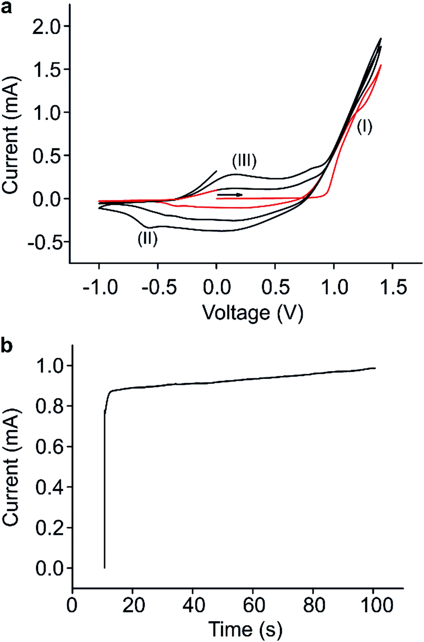 | ||
| Fig. 1 (a) Cyclic voltammetry at a scan rate of 0.1 V s−1 for the oxidation of 0.1 M pyrrole on a 100 μm gap Au IDE on a commercial flexible plastic substrate in 0.1 M LiClO4/acetonitrile for 3 cycles. The red line is the first scan and the black lines are subsequent scans. The crossover point at (I) represents pyrrole growth. The peaks at (II) and (III) represent PPy reduction and oxidation respectively. (b) Chronoamperometric transient obtained for the oxidation of Py in 0.1 M LiClO4/acetonitrile. The potential was stepped from 0 to 1.3 V and held for 90 s. | ||
 | ||
| Fig. 2 Au IDEs with a 100 μm separation on flexible PET substrates (DropSens, Spain). (a) IDE as received and (b) IDE after a 30s PPy deposition. | ||
After polymer deposition, rinsing with CH3CN and drying in air for 10 minutes, the CA process was repeated in a solution devoid of monomer, for 60 s for every sample. This served to p-dope the previously deposited polymer layer with LiClO4, in order to stabilise the polymer and maximise conductance.
Sensing experiments were carried out in a stainless steel cylindrical custom-built gas-sensing chamber, with the following dimensions: internal diameter 21.05 cm, internal depth 9.25 cm, internal volume 3219 cm3. Ammonia gas (500 ppm, nitrogen fill) and N2 gas (for further dilution of NH3) were purchased from BOC gases UK. The flow rates from the respective gas cylinders were controlled by digital mass flow controllers (Alicat, USA) which flow into a Swagelok T-joint to ensure mixing of the gases before entering the inlet of the gas chamber. Total flow rates were fixed at 500 sccm in all cases. The sensors were placed on a sample stage in the chamber with electrical connections running from inside the chamber to a multimeter and power supply outside. The sensing chamber was first purged with nitrogen gas for 45 minutes to remove any impurities present in the chamber or in the sensing layer on the IDEs. Then a voltage of 1 V was applied to the two electrodes and the current was monitored as a function of time on a computer equipped with Benchvue software. Once a stable baseline was reached different concentrations of ammonia gas were allowed into the system. The ppb concentration of ammonia gas that was introduced into the sensing chamber was calculated by the relative flowrates of the two mass flow controllers.
Scanning electron microscopy was performed on the Au IDEs with PPY using a Zeiss Merlin at the David Cockayne Centre for Electron Microscopy (Department of Materials, Oxford University) with an accelerating voltage of 3 kV. The samples were placed on the sample holder without any prior sample preparations (e.g. platinum coating). A special stub from Agar Scientific (SEMClip Specimen mounts) was used to clip the IDEs into place. All images were obtained with secondary electrons.
3. Results and discussion
Sensors were created using CA transient times of 10–90 s, and the conductance of each sensor was measured (Fig. 3(a)). From this, the percolation region could be determined and targeted for the polymer/electrode regime, as detailed in our prior work.26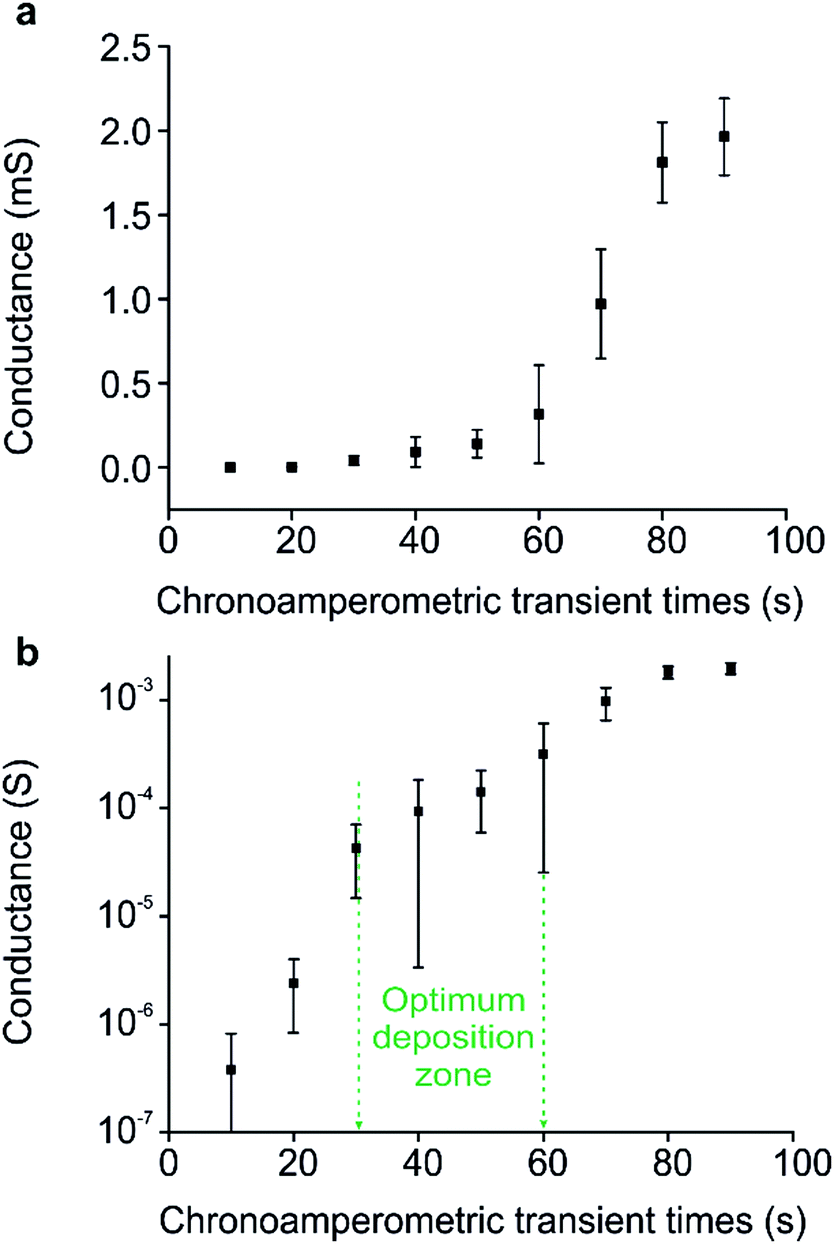 | ||
| Fig. 3 (a) Conductance vs. chronoamperometric transient times for the deposition of polypyrrole on flexible substrate IDEs with 100 μm gaps. Error bars are obtained from the standard deviation of the conductance values of three separate electrode measurements. (b) The semi-logarithmic plot of conductance for the same chronoamperometric transient times. Highlighted in green is the optimum deposition zone, where the lowest LOD values were observed when these networks were used as ammonia sensors. | ||
Initially, the polymer nucleates and grows on the Au electrodes. In our work, this is represented after CA transient times of 10–20 seconds, resulting in MΩ resistance values. Once the metallic electrodes are covered, the polymer continues to grow out into the insulating gaps between the electrodes, steadily forming stable bridges between them. Here, after 30 seconds, a sharp increase in conductance is observed (more easily discernible in the semi-logarithmic plot, Fig. 3(b)). This abrupt increase in gradient is representative of the onset of percolation, where stable connections between Au electrodes begin to form. From this point, the increase in conductivity continues as more connections are made, until a plateau is observed beyond a CA time of 80 seconds. This plateau is characteristic of the point during the deposition when the electrodes are fully connected, and the polymer is in the form of a thin film.
The growth front of polymer with increasing deposition times, can be experimentally observed by considering the SEM images of deposition times from 20–80 seconds (Fig. 4). There are no visible connections after 20–30 seconds (Fig. 4(a) and (b)) of CA deposition, which is consistent with the conductance measurements in Fig. 3. An interesting point to note in Fig. 4(a) and (b), and faintly in Fig. 4(c) is the bright charging effect that is visible between the gaps of the polymer growth fronts. This charging effect is present due to the combination of the insulating nature of the flexible substrates together with the large gap size of 100 μm. This effect is not seen in samples where deposition is carried out beyond 50 seconds. This charging effect, which is usually seen as a negative outcome for imaging, can be used here as an advantage, to visualise conducting bridges forming beyond CA transient times of 40 s.
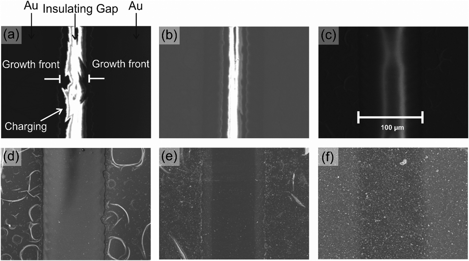 | ||
| Fig. 4 Scanning electron micrographs of a series of Au IDEs with 100 μm separation on flexible substrates, with increasing chronoamperometric transient times from (a) 20 s, (b) 30 s, (c) 40 s, (d) 50 s, (e) 60 s, (f) 80 s, showing increasing polymer coverage both on top of and between electrodes. Images were taken at 3 keV. | ||
After 40 s (Fig. 4(c)) the polymer growth fronts have come into contact, and electrical conductivity increases significantly as a result (reflected in Fig. 3). At 50 s (Fig. 4(d)) it can be seen that the insulating gap is coated with CP. However, when considering the conductance values obtained in Fig. 3, it is clear that conductance commensurate with the thin film region is not reached at 50 s. This is likely due to conductive instability because of the porosity of the PPy film at the intersection between the growth fronts. After 60 s (Fig. 4(e)), a secondary layer of CP begins to grow outwards from the electrodes on top of the previously deposited porous film. Then, from a deposition time of 80 s (Fig. 4(f)), the secondary polymer layer has covered the gap and a stable film of polypyrrole has been deposited. At this point a thin film has been created, consistent with the conductance measurements (Fig. 3).
After identifying the percolation region as a function of CA deposition time for polymer electrochemically deposited on flexible substrates, a new series of chemiresistors were produced, using the same method, with deposition times and thus conductivities representative of various points along the percolation curve. The resulting sensors had resistances of 4.3 MΩ, 430 kΩ, 63 kΩ, 5.7 kΩ, and 760 Ω after 20, 30, 50, 60 and 80 seconds of CA deposition, respectively. They were then exposed to varying concentrations of ammonia gas, from 100 to 700 parts per billion (ppb), in a custom-made gas sensing chamber. PPy is a p-type semiconductor where holes are the major charge-carriers.32 Ammonia is a strong electron-donor that reduces hole density in PPy, thereby causing an increase in the resistance of the sensing polymer upon exposure to the gas.33 In all cases here, an increase in resistance was observed when ammonia gas was allowed in to the sensing chamber, in common with prior studies involving PPy/ammonia interaction.19 The reverse of this process was observed in all cases upon removal of the analyte, when resistance steadily returned to the baseline as weakly bound analyte departed the adsorption sites. The exposure time for each concentration was predetermined at five minutes. The responses decrease linearly with decreasing ammonia concentration for all five chemiresistors investigated.
Each sensor performance could then be analysed to allow a direct comparison of the sensitivity of each sensor, with particular focus on an optimised percolation sensor relative to a thin-film sensor. In this study, the optimum percolation sensor was determined to be the 5.7 kΩ sample, and the thin film was 760 Ω. The response profiles of these two samples can be seen in (Fig. 5(a) and (b), red lines).
 | ||
| Fig. 5 Sensing responses (red lines) and rates of change (blue lines) for PPy chemiresistors on flexible PET substrates in response to 700, 500, 300 and 100 ppb ammonia in a dry N2 carrier gas for (a) the optimum percolation sensor operating at 5.7 kΩ and (b) the thin film 760 Ω sensor. | ||
It is a very common technique to calculate calibration plots using the percentage changes in resistances, peak picking each response with respect to the baseline for varying concentrations. An issue with utilising this method to analyse chemiresistive sensors is that either a fluctuating baseline, or duration of exposure to analyte can influence analysis. For example, exposure for 5 minutes will result in significantly different peak maxima compared with a 10 minute exposure, wherever saturation is not achieved. One method to circumvent this is to analyse the rate of change of the response, obtained by taking the first derivative of each relevant sensing graph (Fig. 5(a) and (b), blue lines). At any point when the resistance signal is not significantly changing over time, the differentiated value returns to zero, ultimately giving access to a zero baseline. In addition, this method of evaluation of sensing data allows for clear visualisation of sensor response for each concentration. The peak in the rate change plot corresponds to the point at which the rate of analyte adsorption is fastest, and thus the gradient of the rate of change in the sensing response is steepest. Consequently, at this point, the sensor is operating at maximum efficiency for each analyte concentration. Taking the root mean square (RMS) of the new zero-centric baseline prior to analyte ingress provides a value for the noise level in the system. Similarly, taking a mean average of the derivative peak maxima over a period corresponding to a ‘linear’ range in the resistance change dataset gives an accurate representation of the signal. A ratio of these two values for each analyte concentration returns the signal to noise ratio (SNR). Once calculated for every analyte concentration, a SNR calibration curve can be plotted (Fig. 6), from which an accurate limit of detection (LOD) can be calculated. In this scenario, the LOD is defined as any signal whose value exceeds three standard deviations from the baseline noise, or when the SNR is greater than 3, and thus a 99% certainty that a signal has been detected.
 | ||
| Fig. 6 Rate of change SNR calibration curves for PPy chemiresistors with different starting resistances on flexible IDEs responding to 100–700 ppb of ammonia. The gradient of these curves corresponds to sensitivity, and is intrinsic to each sensor. | ||
Another benefit of obtaining the rate change data is to aid in the calculation of response times. Response times can be difficult to calculate in instances when the sensing response is changing over time and saturation is not reached. However, since the peak in the rate change data corresponds to the time during which adsorption is occurring at the maximum rate, this can also be used as the optimum response time. In order to calculate response times using this data, values were calculated as the difference between the time of analyte ingress and the time at which the peak maximum occurred for each analyte concentration. The average of these values gives the response time for each sensor over the range of concentrations investigated. Response times in this study ranged from 36 s for the 5.7 kΩ percolation sensor to 78 s for the 760 Ω thin film sensor.
One might think that the optimum sensor should have a resistivity corresponding to the earliest point in the percolation curve, since this represents the point at which the fewest conductive connections exist between electrodes. However, this is also the point at which background noise has the largest negative influence on performance. Owing to the relationship between the absolute sensitivity afforded by the onset of percolation, and the negative impact of background noise, there exists an optimum zone within the percolation region. This optimum zone (highlighted in green, Fig. 3(b)), generally occurs after the initial onset of percolation behaviour, where a stable amount of conducting pathways reduce the influence of noise. By comparison, thin films have an almost limitless number of conductive pathways, resulting in much reduced sensitivity.
In terms of LOD values, the chemiresistors operating at 4.3 MΩ and 760 Ω returned the highest values in this study, of 385 and 158 ppb respectively (Fig. 7). It is interesting to note that both these sensors are operating at the opposing extremes of the percolation profile (Fig. 3). The best sensors investigated here, namely the 5.7 kΩ and 63 kΩ networks, were produced to operate in the optimum zone of the percolation region, where the SNR is highest, and consequently LOD values are lowest, both achieving an LOD of 9 ppb. These sensors were created ranging between 30 s and 60 s of CA deposition. This suggests that a comparatively large window exists in terms of deposition time, where sensors with a relatively large difference in resistance (from 5–100 kΩ) return similar LOD values. This is highlighted in green in Fig. 7, where the optimal range of resistances in terms of low LOD correlates with the optimum deposition zone in the percolation region highlighted in Fig. 3(b).
 | ||
| Fig. 7 Limits of detection for the five PPy sensors investigated. Highlighted in green, the optimal resistance range represents the resistances with the highest sensitivity and lowest LOD, corresponding to the optimum deposition zone of the percolation region. | ||
Other PPy-based thin film and fibre sensors tend to have higher LODs than our sensor, and sub-ppm LODs are rarely achieved.34 Three notable exceptions are reported in the studies. Yan et al.35 reported an LOD of 0.007 ppm using viral-templated gold/PPy nanopeapods, although the R0 baseline was never recovered fully after initial exposure. Chartuprayoon et al.36 achieved a LOD of 0.5 ppm using PPy nanoribbons, and Lee et al.37 who report a minimum detectable level (MDL) of 0.01 ppm using urchin-like nanoparticles decorated with iron oxide nanoneedles. Our LOD of 0.01 ppm (response time range of 36–78 s) therefore places our sensor amongst those chemiresistors able to detect the lowest concentrations of ammonia. Sensitivity is generally determined by plotting a calibration curve of response (ΔR/R0 (%)) against concentration of analyte, where the gradient is the sensitivity. Comparison between sensors of different types from different researchers, tested under different conditions can be difficult to accomplish directly because methods of calculating LODs and sensitivities can vary. Furthermore, ΔR is susceptible to variation dependent upon analyte exposure time and flow rate. R0 can also be difficult to pinpoint if a non-reversible change is occurring alongside the reversible change required for sensor recovery post-exposure, resulting in baseline drift. However, in the interest of comparing our sensor to others, we have attempted to obtain LOD and sensitivity values for a range of PPy-based ammonia sensors from the literature, along with our own. The results are shown in Table 1.
| Material & morphology | Sensitivity ΔR/R0 (%) per ppm NH3 | LOD (ppm) | Response time (s) | Flow rate of analyte gas (sccm) | Ref. |
|---|---|---|---|---|---|
| a Published sensitivity. b Estimated sensitivity from publication. c Non-linear response, gradient estimated from linear portion of the calibration curve. | |||||
| Our work: PPy percolation network on a flexible substrate | 39.4 | 0.01 | 36 (@ <1 ppm) | 500 | This paper |
| Viral templated gold/PPy nanopeapods | 0.30a | 0.007* *R0 value not reached | 900 (@ 5 ppm) | 200 | 35 |
| Urchin-like PPy nanoparticles | 0.95b | 0.01 | <1 (@ 0.1 ppm) | 1–5 | 37 |
| Single PPy nanoribbon | 9.6b | 0.5 | — | 200 | 36 |
| PPy/graphene nanocomposite with titania nanoparticles | 1.22b | 1 | 36 (@ 50 ppm) | — | 38 |
| PPy nanowire arrays | 1.2bc | 1.5 | 60 (@ 77 ppm) | — | 39 |
| Graphene oxide/PPy nanocomposite | 0.12bc | 3 | 400 (@ 3 ppm) | — | 40 |
| PPy thin film | 0.35b | 4 | 20 (@25 ppm) | — | 41 |
It should be noted here that this percolation region is unique for this system, and the percolation region will change according to different CPs and substrates. In this study, the flexible PET substrate surface provides an environment for stable growth as the conducting polymer develops across the insulating gap, resulting in high sensitivities obtained for the detection of ammonia gas, and thus low LODs. This in turn suggests that these commercially available IDEs on flexible substrates represent an ideal platform for chemiresistors operating within the percolation region.
4. Conclusion
In conclusion, we have shown how an electrical percolation network of polypyrrole can be grown between IDEs on a flexible PET substrate. The nature of percolation behaviour in relation to conductivity was supported through SEM imaging of the polymer bridging. Sensors displaying various levels of percolation behaviour were investigated for their sensitivity to interaction with ammonia gas diluted in dry N2. The highest sensitivities and thus lowest LOD values were obtained for the chemiresistors operating within the optimum zone of the percolation region. In this work, the window for production of optimal percolation sensors is large, making reproducibility and thus the potential for large-scale production accessible. Furthermore, the opportunity to extend the utility of these types of percolation sensing layers onto flexible printed electronics and large area sensors is promising. The ability to detect concentrations of ammonia below 10 ppb with a response time under 40 s using electropolymerised sensing layers on flexible substrates results in significant improvements in sensitivity when compared with many competitive PPy deposition strategies, and may open up many routes for utilising percolation sensors in wearable devices.Conflicts of interest
There are no conflicts to declare.Acknowledgements
This research was funded by an EPSRC grant (EP/M015173/1) that supports the Wearable and Flexible Technologies (WAFT) collaboration. The authors thank the Defence Science and Technology Laboratory (DSTL) for financial support. B. A. was funded by an EPSRC DSTL iCASE Award. Contract reference number DSTLX-1000110461.References
- X. Liu, S. Cheng, H. Liu, S. Hu, D. Zhang and H. Ning, Sensors, 2012, 12, 9635–9665 CrossRef PubMed.
- K. L. Gares, K. T. Hufziger, S. V. Bykov and S. A. Asher, J. Raman Spectrosc., 2016, 47, 124–141 CrossRef CAS.
- J. Courbat, M. Pascu, D. Gutmacher, D. Briand, J. Wöllenstein, U. Hoefer, K. Severin and N. F. De Rooij, Procedia Eng., 2011, 25, 1329–1332 CrossRef CAS.
- M. J. Lefferts and M. R. Castell, Anal. Methods, 2015, 7, 9005–9017 RSC.
- E. L. MacLean and B. Hare, Front. Vet. Sci., 2018, 5, 236 CrossRef PubMed.
- R. Blue, D. Uttamchandani, N. Thomson and P. Skabara, in 2015 IEEE SENSORS - Proceedings, IEEE, 2015, pp. 1–4.
- D. H. Read and J. E. Martin, Adv. Funct. Mater., 2010, 20, 1577–1584 CrossRef CAS.
- A. Dey, Mater. Sci. Eng., B, 2018, 229, 206–217 CrossRef CAS.
- C. Wang, S. Lei, X. Li, S. Guo, P. Cui, X. Wei, W. Liu and H. Liu, Sensors, 2018, 18, 3147–3162 CrossRef PubMed.
- T. M. Swager, Macromolecules, 2017, 50, 4867–4886 CrossRef CAS.
- A. Nag, S. C. Mukhopadhyay and J. Kosel, IEEE Sens. J., 2017, 17, 3949–3960 CAS.
- E. Singh, M. Meyyappan and H. S. Nalwa, ACS Appl. Mater. Interfaces, 2017, 9, 34544–34586 CrossRef CAS PubMed.
- Y. Qian, X. Zhang, D. Qi, L. Xie, B. K. Chandran, X. Chen and W. Huang, Sci. China Mater., 2016, 59, 589–608 CrossRef CAS.
- X. Q. Zheng and H. Y. Cheng, Sci. China: Technol. Sci., 2019, 62, 209–223 CrossRef CAS.
- L. Wang, J. Luo, J. Yin, H. Zhang, J. Wu, X. Shi, E. Crew, Z. Xu, Q. Rendeng, S. Lu, M. Poliks, B. Sammakia and C. J. Zhong, J. Mater. Chem., 2010, 20, 907–915 RSC.
- T. Wang, Y. Guo, P. Wan, H. Zhang, X. Chen and X. Sun, Small, 2016, 12, 3748–3756 CrossRef CAS.
- K. E. Brown, M. T. Greenfield, S. D. McGrane and D. S. Moore, Anal. Bioanal. Chem., 2015, 408, 35–47 CrossRef PubMed.
- U. Lange, N. V. Roznyatovskaya and V. M. Mirsky, Anal. Chim. Acta, 2008, 614, 1–26 CrossRef CAS PubMed.
- U. Lange and V. M. Mirsky, Anal. Chim. Acta, 2011, 687, 105–113 CrossRef CAS PubMed.
- B. W. An, J. H. Shin, S. Y. Kim, J. Kim, S. Ji, J. Park, Y. Lee, J. Jang, Y. G. Park, E. Cho, S. Jo and J. U. Park, Polymers, 2017, 9, 303–344 CrossRef PubMed.
- L. Kumar, I. Rawal, A. Kaur and S. Annapoorni, Sens. Actuators, B, 2017, 240, 408–416 CrossRef CAS.
- S. Bai, Y. Zhao, J. Sun, Y. Tian, R. Luo, D. Li and A. Chen, Chem. Commun., 2015, 51, 7524–7527 RSC.
- P. Kuberský, T. Syrový, A. Hamacek, S. Nešpůrek and J. Stejskal, Procedia Eng., 2015, 120, 614–617 CrossRef.
- T. Amaya, Y. Abe, Y. Inada and T. Hirao, Tetrahedron Lett., 2014, 55, 3976–3978 CrossRef CAS.
- V. Kruefu, A. Wisitsoraat, A. Tuantranont and S. Phanichphant, Nanoscale Res. Lett., 2014, 9, 1–12 CrossRef CAS PubMed.
- K. Murugappan and M. R. Castell, Electrochem. Commun., 2018, 87, 40–43 CrossRef CAS.
- H. L. Frisch and J. M. Hammersley, J. Soc. Ind. Appl. Math., 1963, 11, 894–918 CrossRef.
- W.-Y. Diaz, A. F. Castillo, J. I. Logan and J. A. Lee, J. Electroanal. Chem., 1981, 129, 115–132 CrossRef.
- P. N. Bartlett, P. B. M. Archer and S. K. Ling-Chung, Sens. Actuators, 1989, 19, 125–140 CrossRef CAS.
- P. N. Bartlett and S. K. Ling-Chung, Sens. Actuators, 1989, 20, 287–292 CrossRef CAS.
- P. N. Bartlett and S. K. Ling-Chung, Sens. Actuators, 1989, 19, 141–150 CrossRef CAS.
- G. Gustafsson, I. Lundström, B. Liedberg, C. R. Wu, O. Inganäs and O. Wennerström, Synth. Met., 1989, 31, 163–179 CrossRef CAS.
- M. Bazzaoui, J. I. Martins, E. Machnikova, E. A. Bazzaoui and L. Martins, Eur. Polym. J., 2007, 43, 1347–1358 CrossRef CAS.
- Y. C. Wong, B. C. Ang, A. S. M. A. Haseeb, A. A. Baharuddin and Y. H. Wong, J. Electrochem. Soc., 2020, 167, 037503 CrossRef CAS.
- Y. Yan, M. Zhang, C. H. Moon, H. C. Su, N. V. Myung and E. D. Haberer, Nanotechnology, 2016, 27, 1–9 Search PubMed.
- N. Chartuprayoon, C. M. Hangarter, Y. Rheem, H. Jung and N. V. Myung, J. Phys. Chem. C, 2010, 114, 11103–11108 CrossRef CAS.
- J. S. Lee, J. Jun, D. H. Shin and J. Jang, Nanoscale, 2014, 6, 4188–4194 RSC.
- C. Xiang, D. Jiang, Y. Zou, H. Chu, S. Qiu, H. Zhang, F. Xu, L. Sun and L. Zheng, Ceram. Int., 2015, 41, 6432–6438 CrossRef CAS.
- L. Zhang, F. Meng, Y. Chen, J. Liu, Y. Sun, T. Luo, M. Li and J. Liu, Sens. Actuators, B, 2009, 142, 204–209 CrossRef CAS.
- D. C. Tiwari, P. Atri and R. Sharma, Synth. Met., 2015, 203, 228–234 CrossRef CAS.
- A. Joshi, S. A. Gangal and S. K. Gupta, Sens. Actuators, B, 2011, 156, 938–942 CrossRef CAS.
Footnotes |
| † These authors contributed equally. |
| ‡ Current address: Nanotechnology Research Laboratory, Research School of Engineering, Australian National University, Canberra, ACT 2601, Australia. |
| § Current address: Department of Physics, Princeton University, Princeton, NJ 08544, USA. |
| This journal is © The Royal Society of Chemistry 2020 |