
 Open Access Article
 This Open Access Article is licensed under a
 Creative Commons Attribution 3.0 Unported Licence
Embedded-grid silver transparent electrodes fabricated by selective metal condensation†
Silvia
Varagnolo‡
 a,
Keun-Woo
Park
b,
Jin-Kyun
Lee
b and
Ross A.
Hatton
*a
a,
Keun-Woo
Park
b,
Jin-Kyun
Lee
b and
Ross A.
Hatton
*a
aDepartment of Chemistry, University of Warwick, Coventry, CV4 7AL, UK. E-mail: Ross.Hatton@warwick.ac.uk
bDepartment of Polymer Science and Engineering, Inha University, Incheon 22212, South Korea
First published on 16th September 2020
Abstract
We report a new materials system for the fabrication of embedded silver grid electrodes with micron-sized linewidth >10 times narrower than can be achieved using the conventional printing techniques of screen, inject and flexographic printing. Using micro-contact printed thin films of the highly fluorinated polymer poly(3,3,4,4,5,5,6,6,7,7,8,8,9,9,10,10,10-heptadecafluorodecyl methacrylate) together with low temperature heating of the substrate during metal deposition by thermal evaporation, we have fabricated embedded silver transparent grid electrodes on flexible plastic substrates without the need for a metal etching step or a separate grid-embedding step. This simplified approach to grid electrode fabrication is made possible by the very low condensation coefficient of Ag on areas of the substrate covered with the printed organofluorine layer, removing the need for harmful chemical etchants and slow chemical intensive electrochemical deposition steps.
Introduction
Silver (Ag) is one of the most widely used current carrying elements in photovoltaics and displays, and patterned films of this metal are used for a variety of emerging applications including flexible transparent electrodes and as platforms for biological and chemical sensors for point-of-use healthcare and environmental monitoring.1–7 For all of these applications this metal is patterned either by printing from relatively costly colloidal solutions of nanoparticles followed by sintering to fuse the nanoparticles together,8 or by selective removal of metal by etching, which is a slow batch process and uses harmful chemical etchants,9 or by electrochemical deposition.10,11 The latter has the advantage that it enables selective deposition of the metal only where it is needed, but is an inherently chemical intensive and slow process.10,11We have very recently reported a new way to fabricate patterned Cu and Ag films based on local modulation of the metal condensation coefficient, enabled by the finding that Ag and Cu vapour have an extremely small condensation coefficient on films of trichloro(1H,1H,2H,2H-perfluorooctyl)silane (FTS) (Fig. 1a) when the film thickness exceeds ∼10 nm.12 When the FTS layer is printed as a patterned film, metal is deposited only where the highly fluorinated organic layer is not. The beauty of this approach lies in its versatility and simplicity since vacuum evaporation of metals is proven as a low cost method for making thin metal films by the packaging industry, and the shape and dimensions of the features deposited is limited only by the printing method used to deposit the patterned organofluorine layer. This novel approach has a number of advantages: (i) it can be applied to both insulating and conducting substrates; (ii) it uses tiny amounts of organic compounds because the critical thickness (∼10 nm) is two orders of magnitude thinner than the photoresist layers typically used in conventional photolithography; (iii) it avoids the use of harmful metal etchants; and (iv) it can be applied to the top surface of semiconductor devices. Whilst in principle a number of different printing techniques can be used to deposit the organofluorine layer, micro-contact printing is our method of choice for fabricating dense-arrays of micron-sized features of these metals over macroscopic areas, because of its low cost and ease of implementation. Micro-contact printing uses a patterned stamp of polydimethylsiloxane (PDMS) dosed with a thin film of the material to be printed, which is transferred to the substrate when the stamp is brought into contact with the receiving substrate.13 PDMS is used because of its unique elastomer properties, which enables it to make intimate conformal contact with the receiving substrate so that films as thin as one molecular monolayer can be efficiently transferred to the receiving substrate.13
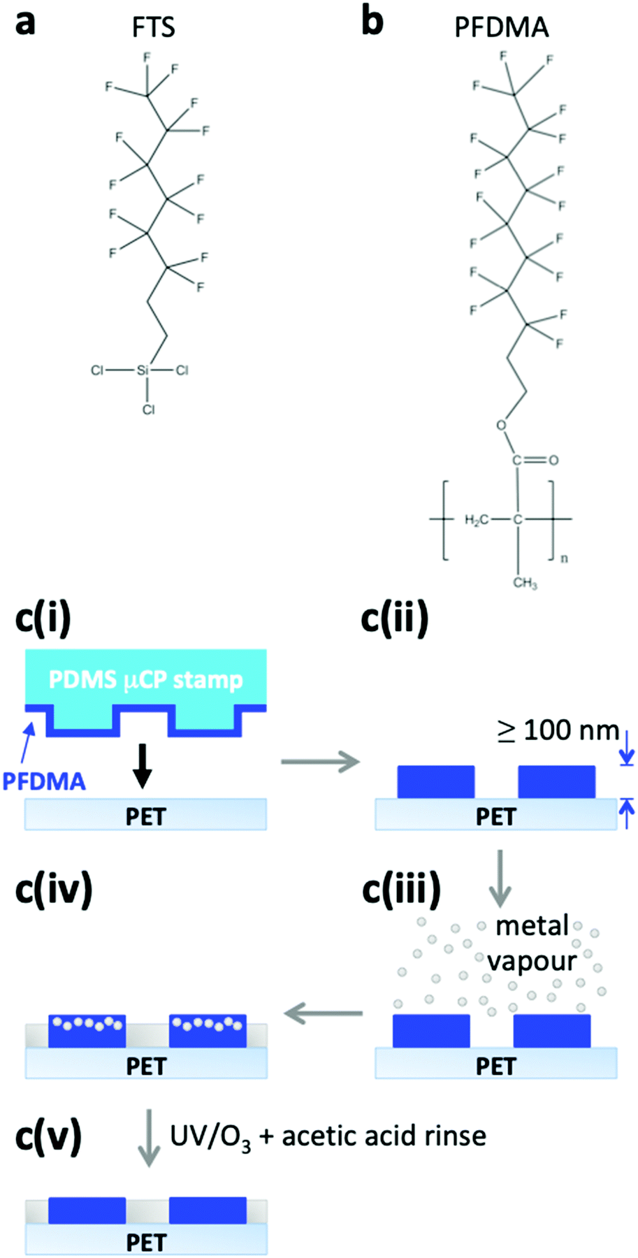 | ||
| Fig. 1 Organofluorine compounds with low condensation coefficient for silver vapour and grid fabrication process. (a) Trichloro(1H,1H,2H,2H-perfluorooctyl)silane (FTS); (b) poly(3,3,4,4,5,5,6,6,7,7,8,8,9,9,10,10,10-heptadecafluorodecylmethacrylate) (PFDMA). (c) Grid fabrication procedure: (i) a polydimethylsiloxane (PDMS) stamp having micron-sized pillars is inked with a PFDMA solution and brought into contact with the polyethylene terephthalate (PET) substrate; (ii) a printed pattern of PFDMA ∼10 nm thicker than the target metal line thickness; (iii) metal deposition over the whole substrate by thermal evaporation under high vacuum (≤10−5 mbar); (iv) formation of a thick metal layer on the uncoated substrate and metal nanoparticles in the polymer layer; (v) removal of the metal nanoparticles by brief UV/O3 treatment followed by acetic acid rinse. | ||
Whilst our first report on this topic demonstrated proof-of-concept, the small highly fluorinated organic molecule FTS has two drawbacks for practical application: (i) the high sensitivity of the chlorosilane moieties on FTS towards reaction with water requires a high degree of control over the water levels both in the solvent used to prepare the FTS solution and the ambient air to ensure the critical film thickness can be achieved over large area; (ii) the number of times the PDMS stamp can be re-used is limited by the propensity of FTS to polymerise particularly when the printed feature sizes are micron-sized. Herein we report a way to circumvent both of these drawbacks based on the use of the highly fluorinated polymer poly(3,3,4,4,5,5,6,6,7,7,8,8,9,9,10,10,10-heptadecafluorodecyl methacrylate) (PFDMA)14 (Fig. 1b) in place of FTS, together with low temperature heating of the substrate during metal deposition. To our knowledge this is only the second literature report pertaining to Ag film patterning by condensation coefficient modulation, an approach that removes the need for harmful chemical etchants, or slow chemical intensive electrochemical deposition steps. Here we demonstrate an improved process that not only circumvents the problems associated with using FTS outlined above, but also enables the fabrication of embedded transparent grid electrodes without the need for a separate grid-embedding step. To demonstrate the power of this approach we have fabricated a grid with a line-width of 1.7 ± 0.2 μm, which is >10 times narrower than can be achieved using industrially relevant printing techniques (e.g. screen, inject and flexographic printing).15
Results and discussion
PFDMA (Fig. 1b) was chosen because it has a high density of perfluoroalkyl moieties along the polymer backbone with a similar structure to the perfluoro tail group on FTS (Fig. 1a), and is amenable to facile micro-contact printing as thin slab-like films of uniform and tunable thickness on a range of substrates.14 Additionally, PFDMA has no highly reactive moieties that could result in cross-linking and clogging of the PDMS stamp during printing, which ensures the stamp can be re-used. For the fabrication of flexible embedded Ag grid electrodes with a metal thickness of 90 nm, a PFDMA film with a thickness of ∼100 nm was micro-contact printed directly onto a flexible polyethylene terephthalate (PET) substrate (Fig. 1c(i) and (ii)), or PET modified with an ultra-thin layer of PEI (polyethylenimine) the latter of which is known to serve as an effective seed layer for evaporated Ag film.16 The substrate was then exposed to Ag vapour in a vacuum evaporator until a total thickness of 90 nm was deposited onto PFDMA-free regions and the adjacent quartz crystal microbalance (Fig. 1c(iii)). Without substrate heating the condensation coefficient (C), determined from the ratio of Ag peak area in the energy dispersive X-ray spectroscopy (EDXS) spectra taken from regions with and without PFDMA, is 0.17 when the metal is deposited at 0.1 nm s−1 (Fig. 2 and Fig. S1, S2, ESI†). This value, which is more than three times higher than previously reported for printed FTS films,12 can be reduced to <0.05 by reducing the metal evaporation rate (Fig. S2, ESI†) although this inevitably increases the time taken to deposit the film. However, by heating the substrate up to 190 °C, which is well below the melting point of PET (255 °C)17 but above the melting point of PFDMA; ∼98 °C (Fig. S3, ESI†), C could be reduced to ≤0.03 without reducing the deposition rate. Indeed it is evident from Fig. 2 that the deposition rate can be increased by ∼3× without incurring an increase in C when this higher substrate temperature is used.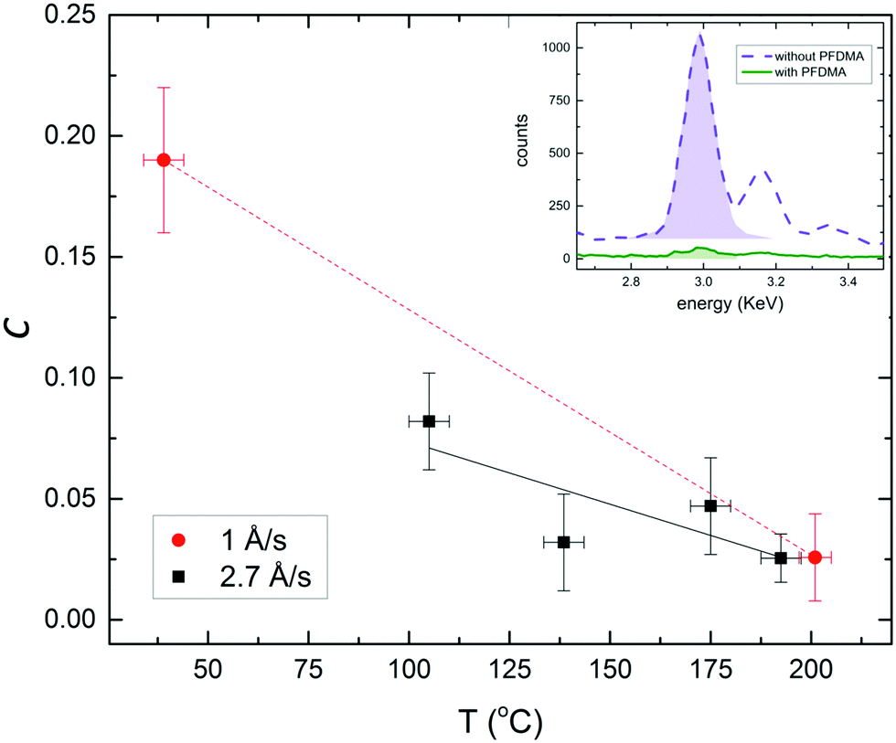 | ||
| Fig. 2 Condensation coefficient, C, of Ag evaporated onto micro-contact printed PFDMA on a PET substrate as a function of the substrate temperature during metal evaporation. Inset: EDXS spectra for the Ag region in areas of the substrate with and without PFDMA. The three peaks refer to X-ray transitions Lα1 (2.98 KeV), Lβ1 (3.15 KeV) and Lβ2 (3.35 KeV). C is determined from the ratio of the Lα1 Ag peak areas. Error bars indicate the maximum error. | ||
Whilst the factors affecting the process of spontaneous desorption of metal atoms, and thus C, from polymer surfaces are still to be fully elucidated,12,18–21 the early stage nucleation studies of Faupel et al.22,23 have shown that even when C is very low there is no direct reflection of the metal atoms from soft surfaces, rather that all metal atoms are initially adsorbed. Given that siloxane linkages are well known for their flexibility,24 and perfluorinated chains interact only very weakly with each other, it is tentatively suggested that the perfluorinated moieties in FTS films move more freely than at the surface of PFDMA which has a more rigid carbon–carbon backbone, and this movement (which is inevitably thermally activated) facilitates the ejection of weakly adsorbed Ag atoms from the polymer surface.
For a Ag thickness of 90 nm deposited onto PFDMA free regions an equivalent of ≤2.7 nm of Ag condenses onto PFDMA coated regions. Even this extremely small amount of Ag couples strongly with the incident light because the Ag atoms aggregate to form nanoparticles (Fig. S4–S7, ESI†), which have a large absorption cross-section due to excitation of an intense localised surface plasmon resonance in Ag.25 Consequently the Ag grids have a coloured tinge, although this is easily removed by brief oxidation with ozone generated using ultra-violet lamp in air (UV/O3) followed by acetic acid treatment to remove the thin silver oxide layer that forms at the surface of the Ag grid. The grid sheet resistance is increased by ≤6% as a result of this treatment. Crucially, this treatment also oxidizes the PFDMA surface, reducing its thickness so that it can be matched to that of the Ag gridline thickness (Fig. S8 and S9, ESI†) whilst also increasing its surface energy so that is can be wetted with solution processed materials typically used to span the grid gaps for electrode applications from polar solvents. To demonstrate the latter we have deposited a poly(3,4-ethylenedioxythiophene):poly(styrenesulfonate) (PEDOT:PSS) and colloidal ZnO overlayers (Fig. S10, ESI†).
To demonstrate the application of this approach we have fabricated embedded 90 nm Ag film grids on PET with an area of 4 cm2 offering an absolute far-field transparency across the wavelength range 400–1100 nm of 77% (Fig. 3a) and sheet resistance of 20 Ω sq−1. It is clear from Fig. 3(a) that ∼11% of the incident light is actually attenuated by the PET substrate, due to reflection and absorption, and so the total transmittance of the grid alone is equivalent to 88%, which is consistent with the 12.7% ± 1.5% metal coverage. The metallized line-width of 1.7 ± 0.2 μm is >10 times narrower than can be achieved using industrially relevant printing techniques such as screen, inject and flexographic printing. Given that the high surface roughness of transparent electrodes based metal grids is widely considered to be limiting for applications in optoelectronic devices based on a thin semiconductor layer such as organic photovoltaics,1 the fact that the grid lines are embedded is a useful feature for application in organic optoelectronics. To test the mechanical strength cyclic bending testing and the Scotch tape peel test were performed: the sheet resistance increased by 1–3% after Scotch tape peel testing and remained unchanged after 5040 bending cycles through 5 mm radius of curvature with the grid under tension, which together provide compelling evidence that the grid is strongly adhered to the supporting substrate.
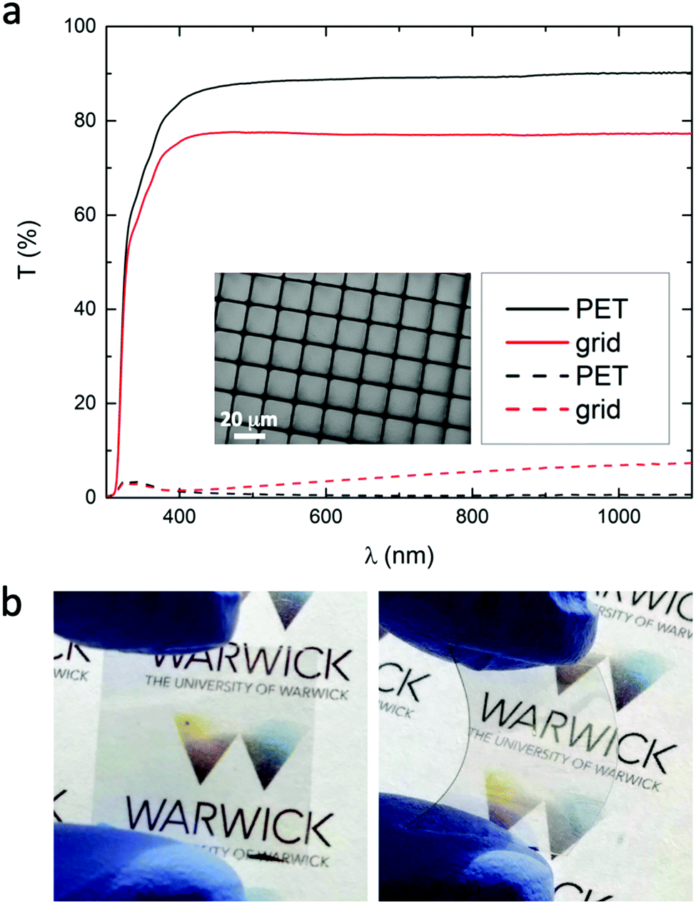 | ||
| Fig. 3 Grid electrodes produced by printing a PFDMA pattern of squares onto 2 × 2 cm2 PET substrates and evaporating 90 nm Ag. The grid lines are 1.7 μm wide and 90 nm thick. The grid spacing is 24.2 μm, which corresponds to 13% metal coverage. (a) Transmittance spectra. Solid lines refer to total transmittance and dashed lines to scattered transmittance. These electrodes have an average absolute transparency across the wavelength range 400–1100 nm of ∼77% although 11% of the incident light is attenuated by the PET substrate due to reflection and absorption, and so the transmittance of the grid alone is equivalent to 88%. (b) Photographs of the 90 nm Ag grid embedded in PFDMA with 1.7 μm linewidth and 24.2 μm grid line separation. | ||
Notably, for the same far-field transparency the sheet resistance of this flexible, embedded Ag grid electrode is lower than can be achieved using PEDOT:PSS,26 carbon nanotube networks27 or multi-layer graphene films,28 and is comparable to that achievable using continuous thin metal films.1 However, there is considerable scope for further optimization of the grid-line spacing and height, as detailed in ref. 15 and 29, and no fundamental reason why performance comparable to the best metal grid electrodes reported to date cannot be achieved, with the advantage that this new fabrication process does not require chemical etchants, complex post-deposition transfer step or a separate grid embedding step.
Conclusion
In summary, we have reported a new material system for the fabrication of Ag grid electrodes by condensation coefficient modulation. Using micro-contact printed thin films of the highly fluorinated polymer poly(3,3,4,4,5,5,6,6,7,7,8,8,9,9,10,10,10-heptadecafluorodecyl methacrylate) (PFDMA) together with low temperature heating of the substrate during metal deposition, we have fabricated embedded transparent grid electrodes on flexible plastic substrates without the need for a separate grid-embedding step and offering a line-width of 1.7 μm. This approach to grid fabrication avoids the use of harmful chemical etchants and slow chemical intensive electrochemical deposition steps. Additionally, PFDMA does not clog the elastomeric stamp used to achieve high resolution grids by micro-contact printing. Given that micro-contact printing is compatible with roll-to-roll processing, and roll-to-roll vacuum evaporation of metals is proven as a low cost method of thin metal film deposition by the packaging industry, this work points the way to a potentially low cost way to fabricate transparent silver grid electrodes with narrow grid line-width and small grid period for myriad potential applications.Author contributions
S. V. performed all of the experiments, except synthesis and characterization of the PFDMA, and co-wrote the manuscript. K.-W. P. and J.-K. L. synthesized and characterized the PFDMA and helped to edit the manuscript. R. H. conceived the study, secured funding for the research and co-wrote the manuscript. All authors have given approval to the final version of the manuscript.Abbreviations
| FTS | Trichloro(1H,1H,2H,2H-perfluorooctyl)silane |
| PFDMA | Poly(3,3,4,4,5,5,6,6,7,7,8,8,9,9,10,10,10-heptadecafluorodecylmethacrylate) |
| PDMS | Polydimethylsiloxane |
| PET | Polyethylene terephthalate |
| SEM | Scanning electron microscopy |
| AFM | Atomic force microscopy |
| EDXS | Energy dispersive X-ray spectroscopy |
Conflicts of interest
The concept reported in this paper is disclosed in the following new UK patent application: ‘Selective deposition of metallic layers’ The University of Warwick, filed 18th October 2018. Application No: 1817037.3.Acknowledgements
The authors kindly thank Mark Crouch (Department of Engineering at the University of Warwick) for the use of the cleanroom facility to produce the silicon masters. The authors would like to thank the United Kingdom Engineering and Physical Sciences Research Council (EPSRC) for funding (Grant number: EP/N009096/1).References
- H. Lu, X. Ren, D. Ouyang and W. C. H. Choy, Emerging Novel Metal Electrodes for Photovoltaic Applications, Small, 2018, 1703140, DOI:10.1002/smll.201703140.
- J. W. Menezes, J. Ferreira, M. J. L. Santos, L. Cescato and A. G. Brolo, Large-Area Fabrication of Periodic Arrays of Nanoholes in Metal Films and Their Application in Biosensing and Plasmonic-Enhanced Photovoltaics, Adv. Funct. Mater., 2010, 20, 3918–3924, DOI:10.1002/adfm.201001262.
- A. Kristensen, J. K. W. Yang, S. I. Bozhevolnyi, S. Link, P. Nordlander, N. J. Halas and N. A. Mortensen, Plasmonic Colour Generation, Nat. Rev. Mater., 2017, 2(1), 16088, DOI:10.1038/natrevmats.2016.88.
- C. Valsecchi, T. Jones, C. Wang, H. Lochbihler, J. W. Menezes and A. G. Brolo, Low-Cost Leukemic Serum Marker Screening Using Large Area Nanohole Arrays on Plastic Substrates, ACS Sens., 2016, 1, 1103–1109, DOI:10.1021/acssensors.6b00368.
- B. Marchiori, R. Delattre, S. Hannah, S. Blayac and M. Ramuz, Laser-Patterned Metallic Interconnections for All Stretchable Organic Electrochemical Transistors, Sci. Rep., 2018, 8(1), 8477, DOI:10.1038/s41598-018-26731-8.
- B. Ai, Z. Wang, H. Möhwald and G. Zhang, Plasmonic Nanochemistry Based on Nanohole, ACS Nano, 2017, 11(October), 12094–12102, DOI:10.1021/acsnano.7b04887.
- J. V. Coe, K. R. Rodriguez, S. Teeters-Kennedy, K. Cilwa, J. Heer, H. Tian and S. M. Williams, Metal Films with Arrays of Tiny Holes: Spectroscopy with Infrared Plasmonic Scaffolding, J. Phys. Chem. C, 2007, 111(47), 17459–17472, DOI:10.1021/jp072909a.
- N. C. Raut and K. Al-Shamery, Inkjet Printing Metals on Flexible Materials for Plastic and Paper Electronics, J. Mater. Chem. C, 2018, 6(7), 1618–1641, 10.1039/C7TC04804A.
- T.-S. Choi and D. W. Hess, Chemical Etching and Patterning of Copper, Silver, and Gold Films at Low Temperatures, ECS J. Solid State Sci. Technol., 2015, 4(1), N3084–N3093, DOI:10.1149/2.0111501jss.
- F.-T. Zhang, L. Xu, J.-H. Chen, B. Zhao, X.-Z. Fu, R. Sun, Q. Chen and C.-P. Wong, Electroless Deposition Metals on Poly(Dimethylsiloxane) with Strong Adhesion As Flexible and Stretchable Conductive Materials, ACS Appl. Mater. Interfaces, 2018, 10(2), 2075–2082, DOI:10.1021/acsami.7b15726.
- L. Zhao, D. Chen and W. Hu, Patterning of Metal Films on Arbitrary Substrates by Using Polydopamine as a UV-Sensitive Catalytic Layer for Electroless Deposition, Langmuir, 2016, 32, 5290, DOI:10.1021/acs.langmuir.6b01118.
- S. Varagnolo, J. Lee, H. Amari and R. A. Hatton, Selective Deposition of Silver and Copper Films by Condensation Coefficient Modulation, Mater. Horiz., 2020, 7(1), 143–148, 10.1039/c9mh00842j.
- J. Tien, Y. Xia and G. Whitesides, Microcontact Printing of SAMs, Thin Films, 1998, 24, 228–250 Search PubMed.
- M. S. Kim, D. H. Lee, Y. H. Cha, K. B. Kim, S. H. Jung, J. K. Lee, O. Beom-Hoan, S. G. Lee and S. G. Park, Preparation of Fluoropolymer Structures for Orthogonal Processing of Diverse Material by Micro-Contact Printing, Microelectron. Eng., 2014, 123, 33–37, DOI:10.1016/j.mee.2014.05.013.
- D. A. Jacobs, K. R. Catchpole, F. J. Beck and T. P. White, A Re-Evaluation of Transparent Conductor Requirements for Thin-Film Solar Cells, J. Mater. Chem. A, 2016, 4(12), 4490–4496, 10.1039/c6ta01670g.
- S. Jeong, S. Jung, H. Kang, D. Lee, S. B. Choi, S. Kim, B. Park, K. Yu, J. Lee and K. Lee, Role of Polymeric Metal Nucleation Inducers in Fabricating Large-Area, Flexible, and Transparent Electrodes for Printable Electronics, Adv. Funct. Mater., 2017, 27(22), 1606842, DOI:10.1002/adfm.201606842.
- J. P. Jog, Crystallization of Polyethyleneterephthalate, J. Macromol. Sci., Polym. Rev., 1995, 35(3), 531–553, DOI:10.1080/15321799508014598.
- T. Tsujioka and K. Tsuji, Metal-Vapor Deposition Modulation on Soft Polymer Surfaces, Appl. Phys. Express, 2012, 5(2), 021601, DOI:10.1143/APEX.5.021601.
- T. Tsujioka, R. Shirakawa, S. Matsumoto, R. Nishimura and K. Uchida, Metal-Vapor Integration/Transportation Based on Metal-Atom Desorption from Polymer Surfaces with a Low Glass-Transition Temperature, J. Vac. Sci. Technol., A, 2017, 35(2), 020603, DOI:10.1116/1.4971415.
- T. Tsujioka, Y. Sesumi, R. Takagi, K. Masui, S. Yokojima, K. Uchida and S. Nakamura, Selective Metal Deposition on Photoswitchable Molecular Surfaces, J. Am. Chem. Soc., 2008, 130(32), 10740–10747, DOI:10.1021/ja802430q.
- T. Tsujioka, Selective Metal-Vapor Deposition on Organic Surfaces, Chem. Rec., 2016, 16(1), 231–248, DOI:10.1002/tcr.201500235.
- V. Zaporojtchenko, T. Strunskus, K. Behnke, C. Von Bechtolsheim, M. Kiene, F. Faupel, T. Strunskus, K. Behnke, C. Von Bechtolsheim, M. Kiene and F. Faupel, Metal/Polymer Interfaces with Designed Morphologies, J. Adhes. Sci. Technol., 2000, 14(3), 467–490, DOI:10.1163/156856100742609.
- A. Thran, M. Kiene, V. Zaporojtchenko, F. Faupel, T. Fakultät and D. U. Kiel, Condensation Coefficients of Ag on Polymers, Phys. Rev. Lett., 1999, 82(9), 1903–1906 Search PubMed.
- M. J. Owen, Siloxane Surface Activity, Silicon-Based Polymer Science, 1989, pp. 705–739 DOI:10.1021/ba-1990-0224.ch040.
- F. S. Ameer, S. Varahagiri, D. W. Benza, D. R. Willett, Y. Wen, F. Wang, G. Chumanov and J. N. Anker, Tuning Localized Surface Plasmon Resonance Wavelengths of Silver Nanoparticles by Mechanical Deformation, J. Phys. Chem. C, 2016, 120(37), 20886–20895, DOI:10.1021/acs.jpcc.6b02169.
- J. Song, G. Ma, F. Qin, L. Hu, B. Luo, T. Liu, X. Yin, Z. Su, Z. Zeng, Y. Jiang, W. Wang and Z. Li, High-Conductivity, Flexible and Transparent PEDOT:PSS Electrodes for High Performance Semi-Transparent Supercapacitors, Polymers, 2020, 12, 450–460, DOI:10.3390/polym12020450.
- L. Yu, C. Shearer and J. Shapter, Recent Development of Carbon Nanotube Transparent Conductive Films, Chem. Rev., 2016, 116, 13413–13453, DOI:10.1021/acs.chemrev.6b00179.
- Y. Ma and L. Zhi, Graphene-Based Transparent Conductive Films: Material Systems, Preparation and Applications, Small Methods, 2019, 3, 1800199, DOI:10.1002/smtd.201800199.
- H. B. Lee, W.-Y. Jin, M. M. Ovhal, N. Kumar and J.-W. Kang, Flexible transparent conducting electrodes based on metal meshes for organic optoelectronic device applications: a review, J. Mater. Chem. C, 2019, 7, 1087–1110, 10.1039/C8TC04423F.
Footnotes |
| † Electronic supplementary information (ESI) available: Experimental procedures and supplementary Fig. S1–S10 (word file). See DOI: 10.1039/d0tc02803g |
| ‡ Present address: School of Engineering and Innovation, The Open University, Milton Keynes, MK7 6AA, UK. |
| This journal is © The Royal Society of Chemistry 2020 |