
 Open Access Article
 This Open Access Article is licensed under a
 Creative Commons Attribution 3.0 Unported Licence
Fermi level pinned molecular donor/acceptor junctions: reduction of induced carrier density by interfacial charge transfer complexes†
Paul
Beyer
a,
Eduard
Meister
b,
Timo
Florian
a,
Alexander
Generalov
c,
Wolfgang
Brütting
 b,
Norbert
Koch
*ad and
Andreas
Opitz
*a
b,
Norbert
Koch
*ad and
Andreas
Opitz
*a
aInstitut für Physik & IRIS Adlershof, Humboldt-Universität zu Berlin, Germany. E-mail: norbert.koch@physik.hu-berlin.de; andreas.opitz@hu-berlin.de
bInstitute of Physics, University of Augsburg, Germany
cMax IV Laboratory, Lund University, Sweden
dHelmholtz-Zentrum Berlin für Materialien und Energie GmbH, Germany
First published on 27th July 2020
Abstract
Increased hole density in an electron donor-type organic semiconductor can be achieved by deposition of a strong acceptor-type molecular layer on top, and has been shown to enable adjusting the carrier density in organic field effect transistors (OFETs). This interfacial charge transfer is due to simultaneous Fermi level (EF) pinning of the donor's highest occupied level and the acceptor's lowest unoccupied level. Here, we investigate the electrical properties of such an EF-pinned junction formed by diindenoperylene (DIP, as donor) and hexafluoro-tetracyano-naphthoquinodimethane (F6, as acceptor) in OFETs, as well as its electronic properties by photoelectron spectroscopy and electrostatic modelling. We find that, in addition to the EF-pinning induced integer charge transfer across the interface, DIP and F6 form charge transfer complexes (CPXs) at their junction. The molecularly thin CPX interlayer acts as insulator and significantly reduces the density of carriers induced on either side of the junction, compared to a scenario without such an interlayer. CPX formation is thus unfavourable for the effectiveness of controlling carrier density at molecular donor/acceptor junctions by EF-pinning.
Introduction
The interest in combinations of electron donor (D) and acceptor (A) molecular materials has significantly grown in the recent past. Prototypical D–A combinations are used in photovoltaic cells,1 exciplex emitters,2 and doped charge transport layers,3 where the occurrence of ground- or excited-state charge transfer (CT) depends strongly on the energy levels of the involved compounds. For ground-state CT, one should recall that either an integer charge can be transferred between D and A or charge transfer complex (CPX) formation can prevail.4 The latter requires significant overlap and hybridization of the D highest occupied molecular orbital (HOMO) and the A lowest unoccupied molecular orbital (LUMO), resulting in a new set of CPX frontier energy levels. Therefore, the CPX exhibits a lower energy gap compared to its parent compounds, and often D–A co-crystals are formed upon mixing D and A. These have been under investigation as narrow gap semiconductors,5 in infrared detectors,6 and the CPX as dopant in organic semiconductor matrices.7Planar two-layer structures of separate D and A on top of each other have been investigated in organic field-effect transistors (OFET),8–11 as this provides for transport channels for both electrons and holes in the two semiconductor layers. It was observed that the threshold voltage in two-layer OFETs differs from the respective single-layer devices, which was related to CT and thus local doping at the D–A interface.8–11 An increased charge carrier density, associated with (partial) filling of trap states can indeed result in a lower threshold voltage.12,13 Electrostatic modelling has highlighted that integer CT at D–A heterojunction interfaces can occur if needed to reach electronic equilibrium, with respective charge accumulation and energy level bending on either side of the junction.14 This type of CT can be long-range and has been described within the framework of Fermi level (EF) pinning,14,15 originally developed for electrode-semiconductor contacts.16,17 This phenomenon has enabled the observation of metallic conductivity at a junction between two molecular D and A single crystals,18 and, more recently, substantial ground-state CT at conjugated polymer heterojunctions.19
However, the analysis of molecular D–A systems is challenging because of the crucial interplay between morphology, energy level alignment, and thus CT.20 Junctions of dissimilar molecules can be fairly sharp and stable,21 while others can undergo local re-orientation22 of molecules or intermixing upon interface formation.23,24 These structural details significantly impact the nature of the CT, and the presence or absence of D–A π-stacking can significantly modify the optical properties of the heterojunction.25,26 Therefore, a comprehensive understanding of D–A heterojunctions is required to relate the fundamental properties to the performance of pertinent devices, and for their improvement.
In this contribution, we demonstrate how two – simultaneously occurring – types of CT (CPX formation and EF-pinning) at a molecular D–A junction modify the charge carrier density distribution across the two layers, and how this impacts the electrical characteristics of corresponding OFETs. This is exemplified for diindenoperylene27,28 (DIP) as donor and hexafluoro-tetracyano-naphthoquinodimethane (F6) as strong electron acceptor;29–31 the chemical structure of both compounds are displayed in Fig. 1a. The reported electron affinity (EA) of F6 thin films (EAF6 = 5.60 eV)32 is higher than the ionisation energy (IE) of DIP thin films (IEDIP = 5.40 eV),33 which would in principle allow integer CT across their interface. However, we note that the formation of a CPX was observed in co-deposited films (i.e., mixed on a molecular scale) of DIP and F6.34,35 The frontier energy levels of DIP, F6, and their CPX [obtained from the present photoelectron spectroscopy (PES) data] are given in Fig. 1b. The influence of D–A junction formation on the electrical characteristics of OFETs was assessed by comparing DIP-based OFETs (Fig. 1c) before and after deposition of a F6 layer. After heterojunction formation we observe clearly improved hole transport, suggesting p-doping of DIP even in the bulk. Finally, with the help of electrostatic modelling, we can explain the hole enrichment throughout the DIP layer by EF-pinning induced CT across the D–A interface, resulting in an electrostatic potential drop over the entire film thickness. The latter moves EF closer to the DIP HOMO level even at the interface to the far-away gate dielectric, i.e., remote p-doping takes place. Furthermore, we find evidence for CPX formation right at the DIP/F6 interface, which, however, significantly reduces hole accumulation in DIP, compared to a scenario without these complexes.
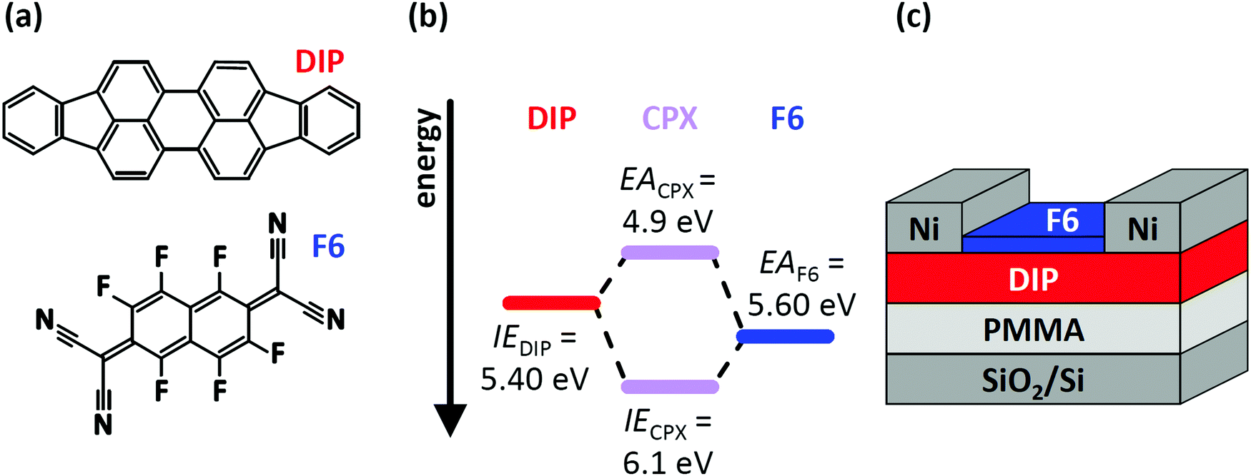 | ||
| Fig. 1 (a) Chemical structure of the organic semiconductor diindenoperylene (DIP) and the acceptor hexafluoro-tetracyano-naphthoquinodimethane (F6). (b) Schematic energy level diagram of DIP, F6 and the formed charge-transfer complex (CPX). Ionisation energy (IE) of DIP and electron affinity (EA) of F6 are taken from literature and were determined by direct and inverse photoelectron spectroscopy.32,33,36,37 (c) Sketch of the device structure for DIP field-effect transistors. The devices were characterised before and after deposition of F6 molecules. | ||
Materials and methods
DIP was purchased from Institut für PAH Forschung (Greifenberg, Germany) and F6 from Novaled (Dresden, Germany). Both materials were used without further purification, and deposited by thermal evaporation. The nominal film thickness was monitored by a quartz microbalance. For OFET measurements, highly p-doped silicon wafers with 300 nm oxide (SiO2, dry oxidation) were covered with 20 nm of poly(methyl methacrylate) (PMMA) as oxide passivation layer,38via spin coating from 1.0 wt% solution in xylene. After deposition of a 25 nm DIP film, nickel electrodes (100 nm) were deposited through a shadow mask. The channel width was 3 mm and the channel length 65 μm. Subsequently, a 5 nm thick F6 layer was deposited on top of the structure to form the D–A interface. PES and near edge X-ray absorption fine structure spectroscopy (NEXAFS) measurements were performed with highly p-doped silicon wafers with a native oxide layer (SiOx, ≈2 nm) as substrate, to avoid sample charging. The same doping type of the applied silicon wafers ensure similar work function and therefore similar electronic behavior. All substrates were solvent cleaned before use.Electrical characterisation was done with a Keithley 4200-SCS under vacuum conditions and using a transfer system in order to prevent devices from ambient exposure. The switch-on voltage39 was determined by the onset of the displacement current, where charge carrier injection and formation of a conductive channel starts.40 The mobilities were estimated from the linear region of the transfer characteristics.41 The area-normalized capacitance (C) of the whole gate insulator stack was determined via impedance measurements of capacitors using a Solartron Dielectric Interface 1296 and a Solartron Impedance/Gain-Phase Analyzer SI 1260.
PES and NEXAFS measurements were performed at the dipole beamline D1011 of the synchrotron storage ring MAX II at MAX IV laboratory (Lund University, Sweden). Ultraviolet photoelectron spectroscopy (UPS) to acquire the valence spectra was performed using a photon energy of 50 eV, and for measurements of the C 1s core level region with X-ray photoelectron spectroscopy (XPS) we used 335 eV excitation. Analyser pass energies of 20 and 50 eV were chosen, respectively. With the SCIENTA SES200 electron energy analyser this gave an experimental resolution of ca. 50 meV for the valence region, as determined from the width of the Fermi edge of a polycrystalline gold sample. The secondary electron cut-off (SECO) spectra were measured with a bias of −26.84 V applied to the sample to overcome the analyser work function. X-ray absorption spectra were obtained by measuring the sample current (total electron yield). For energy calibration a pristine highly oriented pyrolytic graphite (HOPG) sample was used (absorption maximum of the C 1s–π* transition at 285.40 eV).42 All peak positions were determined by fitting Gaussians if not stated otherwise. Core level spectra were fitted using the software XPSPEAK 4.1 applying a combination of Shirley43,44 and linear background.
Optical absorption was measured using a PerkinElmer LAMBDA 950 UV-vis-NIR spectrophotometer in transmission mode using quartz glass substrates. Ex situ scanning force microscopy measurements were performed with a Bruker Dimension Icon in peak force tapping mode (ScanAsyst) and with a NanoWizard 3 AFM by JPK Instruments in standard tapping mode. Background correction and image analysis was done using the software package Gwyddion.45 Electrostatic modelling was performed according to ref. 14 and 46. The parameters used are given in the ESI.†
Results
The transfer characteristics of a DIP-based OFET before and after F6 deposition in the linear regime are displayed in Fig. 2. Both measurements, i.e., without and with the presence of the D–A junction, reveal ambipolar behaviour, as notable source–drain current is detected for electron and hole accumulation, respectively. Bipolar transport in DIP was reported earlier, and even higher electron mobility compared to hole mobility in single crystals27 and OFETs with a passivation layer between silicon oxide gate dielectric and the semiconductor.28,47 After deposition of F6, the curves at negative gate voltage (hole accumulation in DIP) are shifted to less negative voltage. This indicates improved hole accumulation in DIP, which is also expressed in a shift of the switch-on voltage (ΔVSO) by +32 V. The curves for positive gate voltage (electron accumulation in DIP) are shifted to more positive voltage upon D–A junction formation, and ΔVSO is about +6 V. Apparently, electron accumulation in DIP is now less favourable. More details on ΔVSO determination via displacement currents are given in the ESI† (Fig. S1).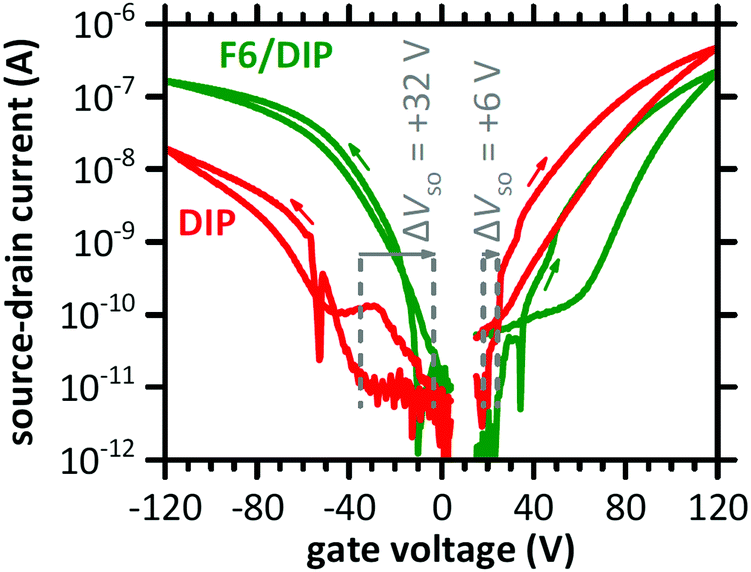 | ||
| Fig. 2 Transfer characteristics of a DIP-based OFET before (DIP) and after deposition of F6 (F6/DIP). The dashed lines indicate the switch-on voltage (VSO) and ΔVSO. The applied drain voltage was +2 V for the electron-transporting and −2 V for the hole-transporting regime. The arrows mark the scan directions. The sudden drops in source–drain current, at −53 V and +35V, are due to the change of accumulated charge carrier type and thus of the sign of current (for the logarithmic scale absolute current values are used). For further details see Fig. S1 (ESI†). | ||
As the switch-on voltage is related to the density of charge carriers at the gate insulator,39,41,48 the change in density of accumulated charge carriers at the gate upon F6 deposition (ΔN) can be calculated by
Further evaluation of the transfer characteristics in the linear regime gives an estimate for the effective charge carrier mobility μh (holes) and μe (electrons),50,51 as summarized in Table 1. After deposition of F6, μh increased ca. threefold while μe decreased to ca. half the value found for DIP alone. Furthermore, for the hole transport regime hysteresis is slightly reduced and in the electron transport regime slightly increased upon D–A junction formation. The changes of mobility and hysteresis are in line with enhanced hole accumulation as concluded on already above from changes of VSO. The higher hole density within DIP enhances the carrier density dependent mobility52,53 and reduces the density of active hole traps.54,55 The opposite holds thus for the electron transport regime. Whereas electrons are the majority charge carriers in the DIP OFET before F6 deposition, the majority changes to holes after F6 deposition. Yet, in the light of the energy offset between IEDIP and EAF6 (see Fig. 1b) that would support CT with high efficiency, it appears remarkable that from OFET characteristics we derive that only one additional out of ca. 170 DIP molecules at the interface to the gate dielectric becomes charged. To obtain further insight into this D–A interface, we performed additional experiments as described in the following.
| Channel | μ h (cm2 V−1 s−1) | μ e (cm2 V−1 s−1) |
|---|---|---|
| DIP | 1 × 10⁻³ | 1 × 10⁻² |
| F6/DIP | 3 × 10⁻³ | 5 × 10⁻³ |
For PES measurements we employ silicon wafers with a native surface oxide layer (SiOx) as substrates to avoid sample charging that would occur for the PMMA/SiO2/Si substrates (as used in OFETs). Thus, we first establish that the morphology and molecular orientation of the D–A junction is comparable on both types of substrates. Scanning force micrographs of DIP films deposited onto PMMA/SiO2/Si and on SiOx/Si are shown in Fig. 3a and b. On both substrates, we observe the typical granular appearance of polycrystalline DIP films, with similar grain size of around 100 nm, as previously reported for comparable films.56 For DIP on PMMA/SiO2/Si, we performed X-ray reflectivity measurements (see ESI,† Fig. S2) and identify the presence of the σ-phase of DIP.33,49 Angle resolved NEXAFS was performed for DIP on SiOx/Si substrates and the π-system of the molecules is oriented at 83° with respect to the surface, which is in accordance with the σ-phase of DIP,21 with molecules essentially upright standing on the substrate. Due to the similarity of the DIP film morphology found for the SiOx/Si substrate we suggest that the same structure and molecular orientation prevails here; furthermore, it is known that DIP molecules exhibit predominantly an upright standing orientation on silicon oxide surfaces.57 Scanning force micrographs of F6 deposited on top of DIP on both substrates are shown in Fig. 3c and d. Once more we find a similar granular morphology for both samples, while the image for the D–A heterojunction on the polymer substrate appears more blurred due to non-ideal tip condition.
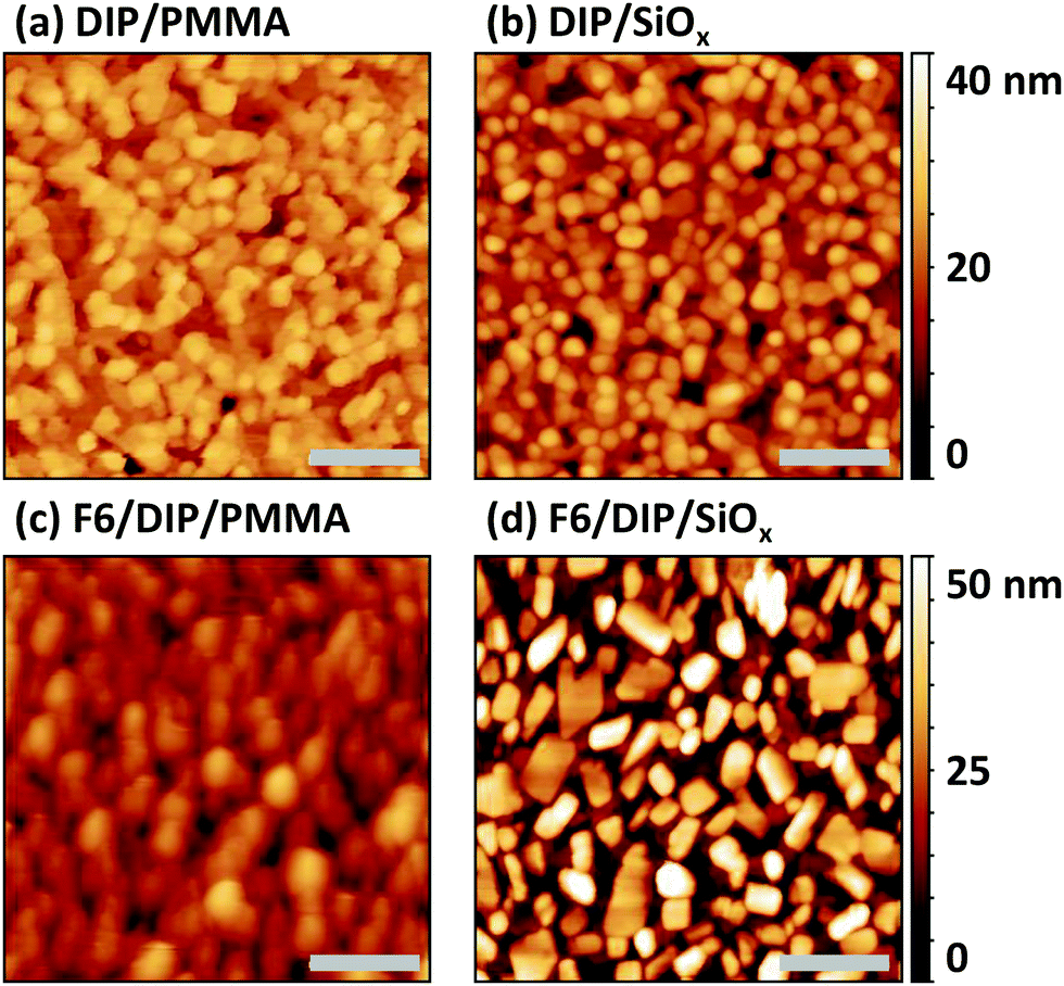 | ||
| Fig. 3 Scanning force micrographs (2 × 2 μm2) for 25 nm DIP on PMMA/SiO2/Si (a) and 30 nm DIP on SiOx (b) as well as for 5 nm F6 on DIP/PMMA/SiO2/Si (c) and 8.5 nm F6 on DIP/SiOx/Si (d). The grey bars indicate a length of 500 nm. | ||
Since we find comparable morphological and structural properties of the DIP and F6/DIP films grown on the two substrates, we proceed with characterizing the electronic properties by PES. The corresponding valence region, the secondary electron cut-off (SECO), and the C 1s core levels spectra are shown in Fig. 4. The work function of the pristine 30 nm thick DIP film is 4.15 eV, equal to the work function we found for the bare SiOx/Si substrate (not shown), and thus vacuum level alignment occurs for the DIP/SiOx interface. The HOMO level onset of DIP is 1.25 eV below the Fermi level (EF) and the resulting IEDIP is 5.40 eV, as also found in literature.33 As the transport gap of DIP was reported to be between 2.25 and 2.60 eV,36,58,59EF is roughly mid-gap for the bare DIP film.
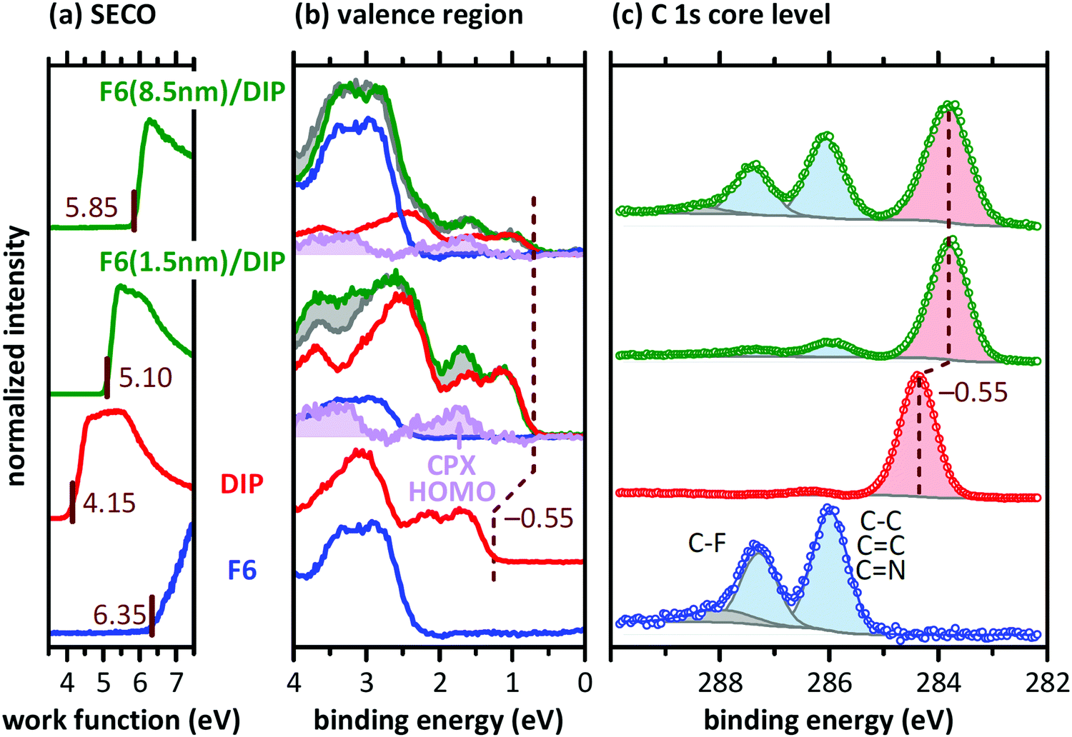 | ||
| Fig. 4 Photoelectron spectroscopy data for pristine F6 and DIP films, as well as for F6 (1.5 nm and 8.5 nm) deposited on the DIP film. (a) SECO spectra, (b) the valence region, and (c) C 1s core level region. After subtraction of the scaled DIP (red) and F6 (blue) spectra from the F6/DIP layered structure (green), the residual signal is attributed to the CPX (purple). The deconvolution of the C 1s spectra shows the contributions of DIP (light red), F6 (light blue) and shake-up satellites (grey). | ||
In contrast, the pristine F6 film exhibits a work function of 6.35 eV and the HOMO onset is ca. 2.35 eV below EF, resulting in an IEF6 of 8.70 eV. Reported IEF6 values in literature vary significantly, between 7.55 eV32 and 8.1 eV.60 These variations in IE are most likely due to differences in the molecular orientation of F6 in the studied samples.59,61 Furthermore, recent theoretical work pointed out that the IE of F6 also shows a strong dependence on the molecular host environment, predicting IEF6 values as high as 8.82 eV.62 However, the high sample work function found here and the high binding energy of the F6 HOMO level are a clear indication that the LUMO level of F6 is pinned at EF.46,63
The C 1s core level spectrum of DIP exhibits a single peak, since all carbon atoms are in a very similar chemical environment. For a pure F6 film we find two well-separated peaks in the C 1s region. The low binding energy component originates from carbons bound to other carbon or nitrogen atoms (C–C, C![[double bond, length as m-dash]](https://www.rsc.org/images/entities/char_e001.gif) C, C
C, C![[triple bond, length as m-dash]](https://www.rsc.org/images/entities/char_e002.gif) N), while the high binding energy component stems from carbon atoms bound to fluorine.64
N), while the high binding energy component stems from carbon atoms bound to fluorine.64
To investigate the formation and electronic properties of the D–A interface, we deposited F6 of two different nominal thicknesses onto DIP. The thickness of 1.5 nm corresponds to ca. a monolayer of F6 and should thus represent the very interface. The higher thickness of 8.5 nm F6 corresponds to multilayer of the acceptor, and is thus representative of a region farther from the interface. Furthermore, the strength of DIP feature attenuation by F6 allows inferring whether a comparably sharp or inter-diffused interface is formed (see discussion of Fig. 5 below). Upon F6 deposition onto DIP, the sample work function increases from 4.15 eV (pristine DIP) to 5.10 eV (1.5 nm F6) and to 5.85 eV (8.5 nm F6). The high work function is comparable to the reported EAF6 of 5.60 eV,32 and thus the F6 multilayer is Fermi level pinned at the LUMO.17 This, in turn, implies that electrons have been transferred from DIP to F6 across the interface. The DIP HOMO level onset shifts by 0.55 eV towards EF upon F6 deposition, which brings it to a position close to or even at being EF-pinned.33 The signatures of DIP and F6 can be clearly identified in the C 1s core level spectrum of the respective samples (Fig. 4c). The binding energy shift of 0.55 eV for the DIP C 1s level parallels that observed for its valence features, evidencing the electrostatic origin of the shift.
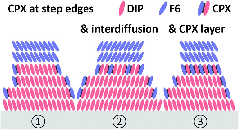 | ||
| Fig. 5 Schemes of possible mechanisms for CPX formation at the corrugated surface of a DIP film in the presence of F6. (1) CPX formation at step edges. (2) additional inter-diffusion of DIP and F6 at the very interface, and (3) possible formation of a CPX interlayer. | ||
In a more detailed analysis, we scaled (in intensity) and shifted (in energy) the valence spectra of pristine DIP and F6 and subtracted these from the valence spectrum of 1.5 nm F6 on DIP. There is a clear residual signal (purple in Fig. 4b) with an onset at 0.7 eV higher binding energy than that of DIP, and its shape does not resemble that of any of the pristine compounds. Therefore, we attribute this signal to the valence spectrum of a CPX formed by DIP and F6, right at the interface. Taking the three spectral signatures (DIP, F6, CPX) obtained in the just described manner, we can adequately reproduce the valence spectrum of 8.5 nm F6 on DIP (with appropriately scaled intensity). Note that the intensity of the CPX signature is lower for 8.5 nm F6 coverage than for 1.5 nm F6 coverage, supporting the notion that the CPX is confined to the very interface. Any signs of CPX formation are not seen in the C 1s core level spectra, as only the frontier orbitals are involved in complex formation.7,65 Considering a symmetric gap opening upon CPX formation7 between DIP and F6, the IE of the CPX is 0.7 eV higher that the IE of DIP (see Fig. 4b), and the EA of the CPX is 0.7 eV lower than the EA of F6, i.e., we obtain IECPX = 6.1 eV and EACPX = 4.9 eV, as shown in Fig. 1b. In contrast to the EF-pinned DIP (at the HOMO) and F6 (at the LUMO) on either side of the junction, the interfacial CPXs appear unpinned. The presence of the CPXs thus adds additional complexity to the electronic structure of the D–A heterojunction.
To provide further support for the presence of CPXs at the F6/DIP interface, optical absorption measurements were performed on a multilayer stack with 10 D–A interfaces to increase the fraction of interfaces in the sample. We find the same low-energy absorption features (at ca. 1.0 and 1.4 eV) that were reported for CPXs of DIP and F6 in co-deposited films where mixing occurred on a molecular scale.34 Furthermore, a CPX-related absorption feature was also detected in X-ray absorption measurements on a two-layer junction. Optical and X-ray absorption data are shown in the ESI† (Fig. S3 and S4). The analysis of molecular orientation from X-ray absorption in the ESI† further shows that the deposition of F6 does not induce a re-orientation of the upright standing DIP molecules.
Since CPX formation requires the overlap of the donor HOMO and acceptor LUMO, both of which are delocalized orbitals in the plane of the molecules, the following morphological considerations are required. When F6 molecules adsorb on the surface of a DIP film with upright standing molecules, orbital overlap and thus CPX formation are precluded. Therefore, mechanisms enabling such orbital overlap must be present. One obvious possibility is, given the granular appearance and relatively high corrugation of the DIP films (Fig. 3), that F6 molecules attach at the edges of DIP grains and form CPXs via the sideways overlap of the two π-electron systems. However, it is unlikely that this is the only CPX enabling mechanism as this would lead to a comparably small fraction of interfacial CPXs only. Fig. 5 shows schematic structures for the appearance of the CPX at the F6/DIP interface. In addition, inter-diffusion of F6 and DIP would also enable orbital overlap and CPX formation. Such a CPX-containing interlayer is most probably confined to one or a few molecular layers near the interface, as our photoemission data (Fig. 4b) reveal a strong attenuation of CPX features by few nm further F6 deposition. Given the high surface sensitivity of photoemission (ca. 1 nm with our experimental parameters), more vertically pronounced intermixing and CPX formation would results in stronger persistence of the diagnostic CPX signal for higher F6 thickness.
Finally, electrostatic modelling of the investigated structures helps to obtain insight into the charge density re-distribution upon D–A junction formation and the electrostatic potential landscape across the multilayer structures, based on experimental parameters. We note that in the 1-dimensional models used here interface corrugation cannot be included, which limits the quantitative significance of the models. Qualitative insight, however, is fully provided and summarized in Fig. 6. Four different structures were investigated: without and with a gate dielectric (insulator) between conductive substrate (degenerately doped Si) and the organic layers to mimic the experimental situation in UPS and OFETs, respectively, and each without and with a monolayer CPX at the interface, to unravel its impact on interfacial charge density. The material parameters used for the models are given in the ESI† (Table S1).
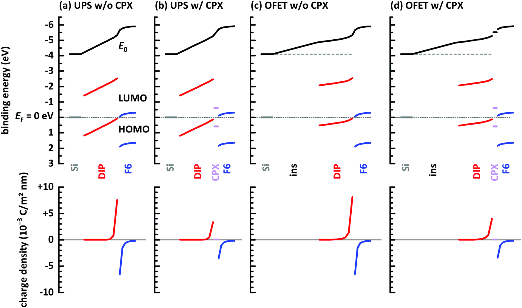 | ||
| Fig. 6 Energy level diagrams obtained from electrostatic modeling,14,46 after reaching electronic equilibrium. (a) Conductive Si/10 layers DIP/7 layers F6 molecules. (b) Same as (a) but with a monolayer CPX between DIP and F6. (c) Conductive Si/20 nm insulator (ins)/10 layers DIP/7 layers F6 molecules. (d) Same as (c) but with a monolayer CPX between DIP and F6. Input parameters for the models are given in ESI.† | ||
First of all, vacuum level alignment holds for all interfaces between DIP film the substrates, since the HOMO and LUMO levels of the organic semiconductor are far away from EF, and flat energy levels prevail in the DIP layer before adding the acceptor layer. This fully agrees with the finding from PES experiments described above. The addition of an F6 layer on top of the four structures then induces significant charge density rearrangements, most notable at the D–A junction. As seen in Fig. 6a, where we excluded the interfacial CPX, the LUMO of F6 is EF-pinned due to electron transfer from DIP, whose HOMO becomes accordingly EF-pinned at the interface. The charges induced on both sides of the interface (shown in the bottom row of Fig. 6) result in space charge layers and the corresponding energy level bending on either side of the junction,66 more clearly seen for the F6 layer. The reason for this is the additional electrostatic potential drop across the entire DIP layer, which is a consequence of the fact that EF is about mid-gap at the bottom interface to Si and it is pinned at the HOMO at the interface with F6. Next, we insert a monolayer of the CPX with its unpinned energy levels at the D–A interface, as shown in Fig. 6b. Charge transfer between DIP and F6 still takes place, as well as the accompanying EF-pinning, energy level bending and electrostatic potential drop across DIP. However, as seen in the bottom part of Fig. 6b, the magnitude of induced charges on either side of the junction is reduced considerably. In essence, the CPX layer acts as a thin insulating interlayer between D and A, which reduces the amount of charge transferred across the interface. In both cases discussed so far, there is virtually no change in charge density at the bottom interface between DIP and the conductive Si.
The latter situation changes notably upon inserting a thick insulating layer (gate dielectric) between the conductive Si and DIP, as shown in Fig. 6c and d, mimicking the situation in an OFET. The insulating layer has a wide energy gap and thus Fermi level pinning is absent for this material. Vacuum level alignment and flat energy level are present in the stack including DIP before addition of the acceptor layer. Upon addition of F6, charge density re-arrangement happens in a mostly analogous manner as described above for Fig. 6a and b. As well, the HOMO and LUMO levels of DIP and F6, respectively, become EF-pinned, energy level bending away from the interface is observed, and an electrostatic potential drop across DIP occurs. However, there is a notable change in the spatial electrostatic potential drop distribution that the gate dielectric insulator is present. Now, the Fermi level is determined on the left-hand side of the structure by the conductive Si contacting the insulator, and on the right-and side by the EF-pinned HOMO level of DIP. Consequently, the electrostatic potential difference between these two positions leads to a potential drop across both the insulator layer and the DIP layer. In turn, this moves the DIP occupied levels closer to EF at any position in the layer, i.e., including the region close to the insulator, as clearly seen in Fig. 6c and d. This is the main reason for the observed increase of accumulated holes ΔN in the OFET (see Fig. 2 and its discussion). Finally, we also observe, in the bottom row plots of Fig. 6c and d, for this case that the insertion of a monolayer CPX between DIP and F6 significantly reduces the induced carrier density on either side of the D–A interface. When aiming at a high density of interface-doping induced charge carriers, the formation of CPXs should thus be prohibited.
Summary
We unravelled the mechanism that leads to increased hole density in the organic semiconductor DIP, next to a gate dielectric in an OFET structure, upon deposition of a molecular acceptor layer on top. Electron transfer from DIP to the acceptor F6 readily occurs across this D–A interface because IEDIP is lower than EAF6. Due to this interfacial integer charge transfer, the HOMO of DIP and LUMO of F6 become EF-pinned at the junction, and energy level bending away from the interface on both sides occurs. In addition, also an interlayer of CPXs containing DIP and F6 molecules is formed, which corresponds to a thin insulator. This, in turn, reduces the density of integer charge transfer across the D–A interface compared to the situation without CPXs, as found from electrostatic modelling. Furthermore, in OFETs the presence of the gate dielectric enhances the acceptor-induced hole density at the DIP/dielectric interface. This is the result of a distributed electrostatic potential drop across the dielectric and the semiconductor layer, which moves the HOMO levels of DIP closer to EF compared to a structure without the dielectric. Our results highlight the importance of the gate dielectric for understanding the spatial carrier density distribution in OFETs that employ D–A interfaces for enhancing the performance. For such structures, however, the formation of CPXs at the interface should be inhibited, as this reduces the beneficial effect of increased carrier density via interfacial charge transfer. A possible acceptor to avoid CPX formation with DIP could be the non-planar molybdenum tris[1,2-bis-(trifluoromethyl)ethane-1,2-dithiolene] [Mo(tfd)3]. Phase separation and the absence of complex formation was reported for co-deposited films of DIP and Mo(tfd)3.67 Finally, we note that similar considerations may be relevant for multilayer OFET channels, and the type of electrostatic modeling employed here can provide valuable insight into the charge distribution in such devices, which, e.g., can achieve superior carrier mobility.68Conflicts of interest
There are no conflicts to declare.Acknowledgements
This work was supported by the Deutsche Forschungsgemeinschaft (DFG) – project 239543752. We are grateful for beamtime at beamline D1011 at Max IV laboratory (Lund, Sweden). We thank Justas Jasiunas for OFET and X-ray reflectivity measurements performed during his internship at the University of Augsburg.References
- C. W. Tang, Appl. Phys. Lett., 1986, 48, 183–185 CrossRef CAS.
- K. Goushi, K. Yoshida, K. Sato and C. Adachi, Nat. Photonics, 2012, 6, 253–258 CrossRef CAS.
- K. Walzer, B. Männig, M. Pfeiffer, K. Leo, B. Maennig, M. Pfeiffer and K. Leo, Highly efficient organic devices based on electrically doped transport layers, American Chemical Society, 2007, vol. 107 Search PubMed.
- I. Salzmann, G. Heimel, M. Oehzelt, S. Winkler and N. Koch, Acc. Chem. Res., 2016, 49, 370–378 CrossRef CAS PubMed.
- R. Sato, M. Dogishi, T. Higashino, T. Kadoya, T. Kawamoto and T. Mori, J. Phys. Chem. C, 2017, 121, 6561–6568 CrossRef CAS.
- B. Siegmund, A. Mischok, J. Benduhn, O. Zeika, S. Ullbrich, F. Nehm, M. Böhm, D. Spoltore, H. Fröb, C. Körner, K. Leo and K. Vandewal, Nat. Commun., 2017, 8, 15421 CrossRef CAS PubMed.
- H. Méndez, G. Heimel, A. Opitz, K. Sauer, P. Barkowski, M. Oehzelt, J. Soeda, T. Okamoto, J. Takeya, J.-B. Arlin, J.-Y. Balandier, Y. Geerts, N. Koch and I. Salzmann, Angew. Chem., Int. Ed., 2013, 52, 7751–7755 CrossRef PubMed.
- Y. Abe, T. Hasegawa, Y. Takahashi, T. Yamada and Y. Tokura, Appl. Phys. Lett., 2005, 87, 1–3 Search PubMed.
- C. Videlot-Ackermann, J. Ackermann and F. Fages, Synth. Met., 2007, 157, 551–557 CrossRef CAS.
- H. Wang, J. Wang, H. Huang, X. Yan and D. Yan, Org. Electron., 2006, 7, 369–374 CrossRef CAS.
- K. Eguchi, M. M. Matsushita and K. Awaga, J. Phys. Chem. C, 2018, 122, 26054–26060 CrossRef CAS.
- F. Hong, F. Xing, W. Gu, W. Jin, J. Zhang and J. Wang, Synth. Met., 2010, 160, 475–478 CrossRef CAS.
- H. Wang and D. Yan, NPG Asia Mater., 2010, 2, 69–78 CrossRef.
- M. Oehzelt, K. Akaike, N. Koch and G. Heimel, Sci. Adv., 2015, 1, e1501127 CrossRef PubMed.
- H. Y. Mao, F. Bussolotti, D. C. Qi, R. Wang, S. Kera, N. Ueno, A. T. S. Wee and W. Chen, Org. Electron., 2011, 12, 534–540 CrossRef CAS.
- P. W. Chye, I. A. Babalola, T. Sukegawa and W. E. Spicer, Phys. Rev. Lett., 1975, 35, 1602–1604 CrossRef CAS.
- J.-P. P. Yang, L.-T. T. Shang, F. Bussolotti, L.-W. W. Cheng, W.-Q. Q. Wang, X.-H. H. Zeng, S. Kera, Y.-Q. Q. Li, J.-X. X. Tang and N. Ueno, Org. Electron., 2017, 48, 172–178 CrossRef CAS.
- H. Alves, A. S. Molinari, H. Xie and A. F. Morpurgo, Nat. Mater., 2008, 7, 574–580 CrossRef CAS PubMed.
- K. Xu, H. Sun, T. P. Ruoko, G. Wang, R. Kroon, N. B. Kolhe, Y. Puttisong, X. Liu, D. Fazzi, K. Shibata, C. Y. Yang, N. Sun, G. Persson, A. B. Yankovich, E. Olsson, H. Yoshida, W. M. Chen, M. Fahlman, M. Kemerink, S. A. Jenekhe, C. Müller, M. Berggren and S. Fabiano, Nat. Mater., 2020, 1–7 Search PubMed.
- A. Opitz, J. Phys.: Condens. Matter, 2017, 29, 133001 CrossRef PubMed.
- U. Hörmann, C. Lorch, A. Hinderhofer, A. Gerlach, M. Gruber, J. Kraus, B. Sykora, S. Grob, T. Linderl, A. Wilke, A. Opitz, R. Hansson, A. S. Anselmo, Y. Ozawa, Y. Nakayama, H. Ishii, N. Koch, E. Moons, F. Schreiber, W. Brütting and W. Brütting, J. Phys. Chem. C, 2014, 118, 26462–26470 CrossRef.
- A. Opitz, A. Wilke, P. Amsalem, M. Oehzelt, R. P. Blum, J. P. Rabe, T. Mizokuro, U. Hormann, R. Hansson, E. Moons and N. Koch, Sci. Rep., 2016, 6, 21291 CrossRef CAS PubMed.
- K. Akaike, N. Koch, G. Heimel and M. Oehzelt, Adv. Mater. Interfaces, 2015, 2, 1500232 CrossRef.
- N. Sai, R. Gearba, A. Dolocan, J. R. Tritsch, W. L. Chan, J. R. Chelikowsky, K. Leung and X. Zhu, J. Phys. Chem. Lett., 2012, 3, 2173–2177 CrossRef CAS PubMed.
- K. Vandewal, Annu. Rev. Phys. Chem., 2016, 67, 113–133 CrossRef CAS PubMed.
- M. Aghamohammadi, A. Fernández, M. Schmidt, A. Pérez-Rodríguez, A. R. Goñi, J. Fraxedas, G. Sauthier, M. Paradinas, C. Ocal and E. Barrena, J. Phys. Chem. C, 2014, 118, 14833–14839 CrossRef CAS.
- A. K. Tripathi and J. Pflaum, Appl. Phys. Lett., 2006, 89, 082103 CrossRef.
- M. Horlet, M. Kraus, W. Brütting and A. Opitz, Appl. Phys. Lett., 2011, 98, 233304 CrossRef.
- P. K. Koech, A. B. Padmaperuma, L. Wang, J. S. Swensen, E. Polikarpov, J. T. Darsell, J. E. Rainbolt and D. J. Gaspar, Chem. Mater., 2010, 22, 3926–3932 CrossRef CAS.
- Y. Karpov, T. Erdmann, M. Stamm, U. Lappan, O. Guskova, M. Malanin, I. Raguzin, T. Beryozkina, V. Bakulev, F. Günther, S. Gemming, G. Seifert, M. Hambsch, S. Mannsfeld, B. Voit and A. Kiriy, Macromolecules, 2017, 50, 914–926 CrossRef CAS.
- B. Lüssem, M. L. Tietze, H. Kleemann, C. Hoßbach, J. W. Bartha, A. Zakhidov and K. Leo, Nat. Commun., 2013, 4, 2775 CrossRef PubMed.
- F. Zhang and A. Kahn, Adv. Funct. Mater., 2018, 28, 1703780 CrossRef.
- J. Wagner, M. Gruber, A. Hinderhofer, A. Wilke, B. Bröker, J. Frisch, P. Amsalem, A. Vollmer, A. Opitz, N. Koch, F. Schreiber and W. Brütting, Adv. Funct. Mater., 2010, 20, 4295–4303 CrossRef CAS.
- G. Duva, L. Pithan, C. Zeiser, B. Reisz, J. Dieterle, B. Hofferberth, P. Beyer, L. Bogula, A. Opitz, S. Kowarik, A. Hinderhofer, A. Gerlach and F. Schreiber, J. Phys. Chem. C, 2018, 122, 18705–18714 CrossRef CAS.
- G. Duva, P. Beyer, R. Scholz, V. Belova, A. Opitz, A. Hinderhofer, A. Gerlach and F. Schreiber, Phys. Chem. Chem. Phys., 2019, 21, 17190–17199 RSC.
- A. Wilke, J. Endres, U. Hörmann, J. Niederhausen, R. Schlesinger, J. Frisch, P. Amsalem, J. Wagner, M. Gruber, A. Opitz, A. Vollmer, W. Brütting, A. Kahn and N. Koch, Appl. Phys. Lett., 2012, 101, 233301 CrossRef.
- H. Méndez, G. Heimel, S. Winkler, J. Frisch, A. Opitz, K. Sauer, B. Wegner, M. Oehzelt, C. Röthel, S. Duhm, D. Többens, N. Koch and I. Salzmann, Nat. Commun., 2015, 6, 8560 CrossRef PubMed.
- N. Benson, C. Melzer, R. Schmechel and H. von Seggern, Phys. Status Solidi, 2008, 205, 475–487 CrossRef CAS.
- E. J. Meijer, C. Detcheverry, P. J. Baesjou, E. Van Veenendaal, D. M. De Leeuw and T. M. Klapwijk, J. Appl. Phys., 2003, 93, 4831–4835 CrossRef CAS.
- Y. Liang, Dissertation, 2011.
- S. M. Sze and D. C. Mattis, Phys. Today, 1970, 23, 75 CrossRef.
- P. E. Batson, Phys. Rev. B: Condens. Matter Mater. Phys., 1993, 48, 2608–2610 CrossRef CAS PubMed.
- D. A. Shirley, Phys. Rev. B: Solid State, 1972, 5, 4709–4714 CrossRef.
- J. Végh, J. Electron Spectrosc. Relat. Phenom., 2006, 151, 159–164 CrossRef.
- D. Nečas and P. Klapetek, Cent. Eur. J. Phys., 2012, 10, 181–188 Search PubMed.
- M. Oehzelt, N. Koch and G. Heimel, Nat. Commun., 2014, 5, 4174 CrossRef CAS PubMed.
- A. Opitz, M. Horlet, M. Kiwull, J. Wagner, M. Kraus and W. Brütting, Org. Electron., 2012, 13, 1614–1622 CrossRef CAS.
- E. J. Meijer, C. Tanase, P. W. M. Blom, E. Van Veenendaal, B. H. Huisman, D. M. De Leeuw and T. M. Klapwijk, Appl. Phys. Lett., 2002, 80, 3838–3840 CrossRef CAS.
- A. C. Dürr, N. Koch, M. Kelsch, A. Rühm, J. Ghijsen, R. L. Johnson, J.-J. Pireaux, J. Schwartz, F. Schreiber, H. Dosch and A. Kahn, Phys. Rev. B: Condens. Matter Mater. Phys., 2003, 68, 115428 CrossRef.
- T. Uemura, C. Rolin, T. H. Ke, P. Fesenko, J. Genoe, P. Heremans and J. Takeya, Adv. Mater., 2016, 28, 151–155 CrossRef CAS PubMed.
- Y. Xu, Y. Li, S. Li, F. Balestra, G. Ghibaudo, W. Li, Y. F. Lin, H. Sun, J. Wan, X. Wang, Y. Guo, Y. Shi and Y. Y. Noh, Adv. Funct. Mater., 2020, 30, 1904508 CrossRef CAS.
- W. F. Pasveer, J. Cottaar, C. Tanase, R. Coehoorn, P. A. Bobbert, P. W. M. Blom, M. De Leeuw and M. A. J. Michels, Phys. Rev. Lett., 2005, 94, 206601 CrossRef CAS PubMed.
- R. Coehoorn, W. F. Pasveer, P. A. Bobbert and M. A. J. Michels, Phys. Rev. B: Condens. Matter Mater. Phys., 2005, 72, 155206 CrossRef.
- Y. Zhang, B. De Boer and P. W. M. Blom, Phys. Rev. B: Condens. Matter Mater. Phys., 2010, 81, 085201 CrossRef.
- S. Olthof, S. Mehraeen, S. K. Mohapatra, S. Barlow, V. Coropceanu, J. L. Brédas, S. R. Marder and A. Kahn, Phys. Rev. Lett., 2012, 109, 176601 CrossRef PubMed.
- A. C. Dürr, B. Nickel, V. Sharma, U. Täffner and H. Dosch, Thin Solid Films, 2006, 503, 127–132 CrossRef.
- S. Kowarik, A. Gerlach, S. Sellner, F. Schreiber, L. Cavalcanti and O. Konovalov, Phys. Rev. Lett., 2006, 96, 125504 CrossRef CAS PubMed.
- S. Krause, A. Schöll and E. Umbach, Org. Electron., 2013, 14, 584–590 CrossRef CAS.
- W. N. Han, K. Yonezawa, R. Makino, K. Kato, A. Hinderhofer, R. Murdey, R. Shiraishi, H. Yoshida, N. Sato, N. Ueno and S. Kera, Appl. Phys. Lett., 2013, 103, 253301 CrossRef.
- M. Hantusch, R. Kuhrt and M. Knupfer, J. Phys. Chem. C, 2020, 124, 2961–2967 CrossRef CAS.
- S. Duhm, G. Heimel, I. Salzmann, H. Glowatzki, R. L. Johnson, A. Vollmer, J. P. Rabe and N. Koch, Nat. Mater., 2008, 7, 326–332 CrossRef CAS PubMed.
- J. Li, I. Duchemin, O. M. Roscioni, P. Friederich, M. Anderson, E. Da Como, G. Kociok-Köhn, W. Wenzel, C. Zannoni, D. Beljonne, X. Blase and G. D’Avino, Mater. Horiz., 2019, 6, 107–114 RSC.
- H. Wang, P. Amsalem, G. Heimel, I. Salzmann, N. Koch and M. Oehzelt, Adv. Mater., 2014, 26, 925–930 CrossRef CAS PubMed.
- C. Christodoulou, A. Giannakopoulos, G. Ligorio, M. Oehzelt, M. Timpel, J. Niederhausen, L. Pasquali, A. Giglia, K. Parvez, K. Müllen, D. Beljonne, N. Koch and M. V. Nardi, ACS Appl. Mater. Interfaces, 2015, 7, 19134–19144 CrossRef CAS PubMed.
- I. Salzmann, G. Heimel, S. Duhm, M. Oehzelt, P. Pingel, B. M. George, A. Schnegg, K. Lips, R.-P. P. Blum, A. Vollmer and N. Koch, Phys. Rev. Lett., 2012, 108, 035502 CrossRef PubMed.
- J. X. Tang, C. S. Lee and S. T. Lee, J. Appl. Phys., 2007, 101, 064504 CrossRef.
- A. Opitz, C. Peter, B. Wegner, B. Wegner, H. S. S. S. S. R. Matte, A. Röttger, T. Florian, X. Xu, P. Beyer, L. Grubert, S. Hecht, V. Belova, A. Hinderhofer, F. Schreiber, C. Kasper, J. Pflaum, Y. Zhang, S. Barlow, S. R. Marder, N. Koch and N. Koch, J. Phys. Chem. C, 2020, 124, 11023–11031 CrossRef CAS.
- P. Zhang, H. Wang and D. Yan, Adv. Mater., 2017, 29, 1702427 CrossRef PubMed.
Footnote |
| † Electronic supplementary information (ESI) available: Source-gate current measurements, additional structural data from X-ray reflectivity and scanning force microscopy, absorption spectra, angle dependent NEXAFS deconvolution, parameters used for electrostatic modelling. See DOI: 10.1039/d0tc02774j |
| This journal is © The Royal Society of Chemistry 2020 |