
 Open Access Article
 This Open Access Article is licensed under a Creative Commons Attribution-Non Commercial 3.0 Unported Licence
Ga2O3 polymorphs: tailoring the epitaxial growth conditions
M.
Bosi
 *a,
P.
Mazzolini
b,
L.
Seravalli
a and
R.
Fornari
ab
*a,
P.
Mazzolini
b,
L.
Seravalli
a and
R.
Fornari
ab
aIMEM-CNR, Viale delle Scienze 37/A, 43124 Parma, Italy. E-mail: matteo.bosi@imem.cnr.it
bDepartment of Mathematical, Physical and Computer Sciences, University of Parma, Viale delle Scienze 7/A, 43124 Parma, Italy
First published on 14th July 2020
Abstract
Gallium oxide is a wide bandgap n-type semiconductor highly interesting for optoelectronic applications (e.g., power electronics and solar blind UV photodetectors). Besides its most thermodynamically stable monoclinic β phase, Ga2O3 can crystallize in different polymorphs; among them the corundum α and the orthorhombic ε phases are the most promising ones. In this review we focus on the main aspects that promote the nucleation and stable growth of these Ga2O3 polymorphs. Particular emphasis is given to the ε phase since it is recently gaining increasing attention in the scientific community because of: (i) its higher lattice symmetry with respect to β-Ga2O3, which could favour the realization of heterostructures, (ii) the possibility to be grown on cheap sapphire substrates and (iii) its peculiar piezoelectric properties. While the growth of β-Ga2O3 is widely studied and understood, a thorough and comprehensive analysis of the chemical and physical aspects that allow for the stabilization of the metastable Ga2O3 phases with different synthesis methods is still missing. Therefore, the present review aims at filling this gap, by analysing the relevant growth parameters for several growth techniques (MOVPE, HVPE, mist-CVD, MBE, and PLD), highlighting similarities and differences, looking for a unified framework to understand the growth and nucleation of different Ga2O3 polymorphs. As a conclusion, we highlight practical guidelines for the deposition of the different Ga2O3 polymorphs with all the discussed thin film growth techniques.
 M. Bosi | The scientific activity of Dr Matteo Bosi has always been focused on epitaxial deposition by means of Metal Organic Vapor Phase Epitaxy (MOVPE) of semiconductor materials for photovoltaic, sensor and optoelectronic devices. During his career he has studied the epitaxy/synthesis of arsenides and phosphides (GaAs, InGaP, and AlGaAs), germanium, SiC, diluted nitrides (GaAsN) and III-nitrides (GaN and InGaN), nanowires (Ge and SiC) and transition metal dichalcogenides (MoS2), and oxides (TiO2 and Ga2O3). During his career Dr Matteo Bosi has attended about 20 international conferences with several invited talks and he is author or co-author of about 100 papers in international peer-reviewed journals. |
 P. Mazzolini | Piero Mazzolini joined the group of Prof. R. Fornari as a researcher in 2020, Italy. He graduated in “Materials Engineering” at the University of Trieste in 2012. He received his PhD in “Energy and Nuclear Science and Technology” at the Politecnico di Milano in 2015 working on doped oxide thin films for transparent electronics (Ta-doped TiO2). For his master's thesis and during his PhD he visited the Max Planck Institute for Solid State Research of Stuttgart. As a postdoc at the Paul Drude Institute in Berlin he worked on the molecular beam epitaxial growth of Ga2O3/In2O3 thin films in the research group of Dr O. Bierwagen. |
 L. Seravalli | Luca Seravalli is a researcher at IMEM-CNR. He received a MSc in physics at Trinity College of Dublin in 2000 and a PhD in physics at the University of Parma in 2003. From 2001 he has been working on epitaxial growth, optical characterization and modelization of semiconductor nanostructures. He has authored 80 articles with over 1000 citations and he has an h-index of 19. His current interests include MOVPE growth of Ga2O3 and of Ge nanostructures and CVD growth of 2D materials. |
 R. Fornari | Roberto Fornari is Full Professor of Condensed Matter Physics at Parma University (Italy), where he also serves as Vice-Rector for Research. Prior to joining Parma University in 2013, he was Director of the Leibniz-Institut für Kristallzüchtung (IKZ) and professor at the Humboldt University, Berlin (2003–13), and research scientist at the Institute of Materials for Electronics and Magnetism (IMEM-CNR; 1981–2003). He has authored/co-authored over 170 articles in international journals, ten patents and several book chapters on semiconductor physics and technology. He served as President of the Intern. Organization for Crystal Growth (2010–16); in the Europ. Materials Research Society (Exec. Committee, 2011–17), and as associate editor of four scientific journals. |
1. Introduction
Metal sesquioxides are very interesting semiconducting materials that have attracted much attention in the last decade. Gallium oxide (Ga2O3) has especially become popular because of its intrinsic properties: very wide bandgap (Eg > 4.5 eV) and high critical breakdown field, estimated to be about 8 MV/cm, higher than that of other wide bandgap materials like SiC and GaN.1 This makes gallium oxide a promising candidate for high power electronics, with a field of applications complementary to the ones of SiC and GaN. Additionally, its extra-wide bandgap makes this semiconductor suitable for fabrication of solar-blind detectors for UV-C radiation (wavelength below 280 nm).It must however be mentioned that generically talking about Ga2O3 can be misleading, as this material has five polymorphs of which only one is thermodynamically stable at high temperatures (β phase, monoclinic), while the others are metastable and tend to convert to β upon high-temperature treatments. The first study on polymorphism of Ga2O3 dates back to 19522 and reported two novel polymorphs: δ, cubic, and ε, hexagonal, in addition to the already known α, corundum, and γ, defective-spinel, phases. In a later crystallographic study, Playford et al.3 introduced also the κ polymorph, which brought the total number of explored polymorphs to six. It is to be noted that the used nomenclature follows the existing one for the more investigated aluminum oxide Al2O3.
So far, most attention was concentrated on the thermodynamically stable β-Ga2O3 phase, essentially for one reason: it can be grown both as a single crystal and as a thin epitaxial layer, thus enabling homoepitaxy and permitting one to lower the density of structural defects. Alloys with Al or In can modulate the β-Ga2O3 bandgap,4,5 allowing for the realization of heterostructures and the formation of a modulation doped 2D electron gas (2DEG) at the heterojunction, enabling high performance electronics. However, this phase presents also evident drawbacks, essentially due to the highly-asymmetric monoclinic structure. This implies a remarkable anisotropy of thermal conductivity6 and of optical properties,7 alongside a relatively mild anisotropy of electrical properties.8 Furthermore, bulk β-Ga2O3 is prone to cleavage and homoepitaxially-grown epilayers on certain crystal orientations – e.g., (100)9 – were surprisingly seen to suffer from a high density of twin lamellae, part of which may lead to incoherent twin boundaries with dangling bonds, which may act as acceptors, thus limiting the n-type doping and electron mobility. This problem could be overcome either by growing on 4–6° off-oriented (100) substrates,10 a methodology that proved to be effective but that ultimately makes the homoepitaxy less attractive, or by selecting a different substrate orientation for the homoepitaxy like (010)11 or (001).12,13
For the above reasons, in the past few years Ga2O3 research has been extended towards the two phases that present higher symmetry and easier epitaxial conditions than β-Ga2O3, namely α and ε. Their main properties are summarized in Table 1. Both polymorphs were obtained by a variety of epitaxial techniques on different hetero-substrates, mostly sapphire, as well as on β-Ga2O3. Our research team, including researchers from IMEM-CNR and Dept. of Mathematical, Physical and Computer Sciences of Parma University, has been one of the first worldwide to undertake extensive research activity on ε-Ga2O3: we reported for the first time in 2016 on the Metal Organic Vapor Phase Epitaxy (MOVPE) epitaxial growth of single-phase ε-type layers on c-oriented sapphire, (0001)-oriented GaN and (111)-oriented cubic SiC.14 Our interest in the ε material at that time was mostly motivated by the easier epitaxial deposition conditions, more uniform physical properties and higher crystallographic symmetry with respect to β-Ga2O3. Furthermore, we detected unusual properties, such as ferroelectricity,15 which were also theoretically confirmed by Maccioni and Fiorentini,16 and Cho and Mishra.17 Indeed, films of ε-Ga2O3 are generally deposited at much lower temperature, while their spontaneous c-oriented polarization may be exploited for designing and manufacturing novel hybrid devices. This was recently confirmed by Leone et al., who reported on the epitaxial growth of GaN/Ga2O3 and ε-Ga2O3/GaN heterostructures for novel high electron mobility transistors.18 ε-Ga2O3 alloys with In and Al were obtained with mist Chemical Vapor Deposition (mist-CVD) and Pulsed Laser Deposition (PLD),19,20 while a theoretical study21 demonstrated the possibility to form a 2D electron gas at the ε-AlGaO3/ε-Ga2O3 heterointerface with higher carrier density with respect to β-Ga2O3 and the effect of spontaneous polarization reversal on the 2D electron gas density in ε-Ga2O3/ε-AlGaO3/ε-Ga2O3 double heterostructures.
| β-Ga2O3 | α-Ga2O3 | ε-Ga2O3 | |
|---|---|---|---|
| Bandgap (Eg) | 4.9 | 5.2 | 4.9 |
| Structure | Monoclinic (C2/m) | Corundum (R![[3 with combining macron]](https://www.rsc.org/images/entities/char_0033_0304.gif) c) c) |
Orthorhombic (P63mc) |
| Dielectric constant εr | 10 | 10 | |
| a (Å) | 12.214 | 4.983 | 29.067 |
| b (Å) | 3.037 | ||
| c (Å) | 5.798 | 13.433 | 9.255 |
| β (degrees) | 103.83 | ||
| Theoretically predicted RT electron mobility (cm2 V−1 s−1) | 300 |
After the pioneering work on deposition of ε-Ga2O3 on sapphire, our group also dedicated much attention to the investigation of the physical properties and suitable doping procedures for this polymorph.22–24 After confirming that the bandgap of the ε phase is comparable with that of β-Ga2O3, attention was also turned to potential applications in the area of solar-blind UV photodetectors.25 All this evidence provides the motivation for continuing the work on ε-Ga2O3 and also for the present review.
Before starting examining the growth conditions of ε-Ga2O3 it is however necessary to clear an ambiguity that has confused, and to some extent still confuses, the Ga2O3 community: what is exactly the ε phase and how does it relate to the orthorhombic κ phase? Historically the ε phase has been considered to be purely hexagonal.3,15,26 This is to be ascribed to the used investigation methods, neutron or X-ray diffraction, which, owing to their inherent resolution, suggested ε-Ga2O3 to have hexagonal crystal structure with space group P63mc. It was some years later that Cora et al.27 examined the microstructure of MOVPE-grown ε-Ga2O3 on (0001) sapphire by high-resolution TEM: they found that the film was indeed “pseudo-hexagonal” as the apparent hexagonal symmetry actually resulted from in-plane 120° rotational nano-domains of orthorhombic Ga2O3. They corrected the space group to Pna21 and, in analogy with Al2O3, suggested this polymorph to be more properly named κ. More recently these findings were confirmed by Nishinaka et al.28 In other words, it is possible to obtain phase-pure ε-Ga2O3 but one has to be aware that it is not single crystalline; rather it is composed of tiny (201) domains of orthorhombic Ga2O3 separated by 120° twins, virtually with no dangling bonds. It is the short-range order of the gallium octahedra and tetrahedra included between the oxygen planes that gives rise to such a particular arrangement. When studied by X-ray diffraction this structure provides diffraction patterns compatible with a hexagonal structure, but it reveals an orthorhombic structure when investigated with a probe of higher resolution. The scientific community should therefore more correctly speak of “orthorhombic ε-Ga2O3” or rather “pseudo-hexagonal ε-Ga2O3”, remembering however that the intimate, microscopic structure is actually orthorhombic κ.
The other technologically important Ga2O3 polymorph, α, exhibits a bandgap of 5.3 eV, even higher than β-Ga2O3 and ε-Ga2O3. Ternary alloys (AlxGa2−x)O3 could be obtained in a wide range of composition, facilitating band engineering and fabrication of hetero-structured devices. α-Ga2O3 shares the same corundum structure as α-Al2O3 and it does not exhibit the rotational domain problems typical of ε- and β-Ga2O3.29 Moreover, the possibility to obtain p-type doped α-Ir2O3 and α-Rh2O3 permits in principle the realization of p–n corundum-structured heterojunctions on α-Al2O3. In terms of applications, photodetectors30 and metal-oxide semiconductor field-effect transistors using a hetero-pn-junction31 have already been demonstrated.
Being less mature and less studied than the β phase, some physical properties of the α and ε polymorphs are still not precisely known. For example, while the maximum theoretical breakdown field of β-Ga2O3 is estimated to be as high as 8 MV cm−2,32 to the best of our knowledge no similar estimates are present for α- and ε-Ga2O3. Similarly, for β-Ga2O3 the room temperature electron mobility upper limit is theoretically predicted to be around 300 cm2 V−1 s−1 (Table 1), while no clear estimates of the upper limit of the electron mobility are available for both α and ε. Therefore, even if some theoretical studies investigated the structural, electronic, and optical properties of the polymorphs,33,34 we believe that more effort is needed in order to unveil their full potential from both a theoretical and an experimental point of view.
We already pointed out in the previous paragraphs the possibilities given by bandgap engineering to modulate the bandgap of Ga2O3 with In and Al, permitting the realization of ternary alloys with bandgaps varying ideally between 3.7 (In2O3)4 and 8.8 (Al2O3)35 eV. Heterostructures based on these alloys could dramatically expand the possibilities for the design of novel devices. However, while the technology for β-Ga2O3 ternary alloys is quite advanced and it was already discussed in several papers and books,1,36 the literature of α- and ε-Ga2O3 ternary alloys is still quite limited, making an in-depth discussion on this topic premature and beyond the scope of this review.
The last remark concerns the actual thermal stability of the α and ε polymorphs. By combining TEM and X-ray diffraction with differential scanning calorimetry, Fornari et al. demonstrated that ε-Ga2O3 initiates a structure modification at about 700 °C and fully converts to β-Ga2O3 when it is annealed at temperatures above 900 °C.37 Very recently, Cora et al. performed TEM analysis on ε-Ga2O3 subjected to thermal treatments at different heating rates and they were able to detect in real time the phase transition.38 Annealing experiments up to 1000 °C were performed either in situ in a vacuum inside the TEM chamber, or ex situ in ambient air. The TEM observations provided a real time view of the atomistic re-arrangement at the basis of the κ to β phase transition. Surprisingly, the ex situ experiments instead demonstrated the formation of an additional γ-Ga2O3 phase at 820 °C. The different behaviour between in situ and ex situ annealing experiments was explained in terms of the atmosphere (ambient air or high vacuum) and heating rate. Regarding α-Ga2O3, Lee et al.39 demonstrated that α-Ga2O3 films grown at 470 °C by mist-CVD are stable until 550 °C, but are gradually changed to the β-phase after annealing in an N2 atmosphere for 60 minutes at temperatures higher than 600 °C.
In this work, by comparing numerous experimental data from different epitaxial methods, we would like to extend the understanding of the nucleation and stable growth of Ga2O3 polymorphs, especially focusing on the synthesis of ε and α layers. A thorough assessment of the information published to date allows us to identify the critical parameters for phase selection. For a long time it has been indeed puzzling that growth under similar conditions did result in either α or ε films, or that a certain polymorph could be obtained with one growth technique and not with another. To the best of the authors’ knowledge, no effort has been made to understand the reason for this behaviour and to critically analyse the literature on ε/α-Ga2O3 growth with different techniques. We believe that a deeper understanding of the growth mechanisms of Ga2O3 could help the progress of its different polymorphs and be therefore beneficial to the entire Ga2O3 community.
2. Growth of Ga2O3 polymorphs
In Table 2 we collected several papers related to the growth of different Ga2O3 polymorphs by the most common techniques: MOVPE, mist-CVD, Halide Vapor Phase Epitaxy (HVPE), Molecular Beam Epitaxy (MBE), and PLD. We included papers in which the growth parameters were explicitly mentioned and discussed, with emphasis towards the gas flows and/or the ratio of the reagents used in the deposition. We also decided to highlight articles in which different Ga2O3 phases were obtained by changing the synthesis parameters in different growth runs on the very same growth setup (collected in cells arranged in the same row). In the table we listed the following parameters: substrate and orientation, reagent types, and growth temperature, as well as notes for specific cases. For an overview of the above mentioned growth techniques the reader is referred to specific reviews and books, as a detailed description of each growth process is beyond the scope of this work.1,40,41| HVPE | ||
|---|---|---|
| α | β(![[2 with combining macron]](https://www.rsc.org/images/entities/char_0032_0304.gif) 01) 01) |
ε |
c-Plane sapphire; GaCl + O2, HCl (0.37% total flow), HCl![[thin space (1/6-em)]](https://www.rsc.org/images/entities/char_2009.gif) :O2 = 0.25; Tg = 650 °C.53 :O2 = 0.25; Tg = 650 °C.53 |
c-Plane sapphire; GaCl3 +O2, HCl (0.71% total flow), HCl:O2 = 0.07; Tg = 850 °C.53 |
c-Plane sapphire; GaCl3 + O2, HCl (0.69% total flow), HCl:O2 = 0.05; Tg = 650 °C.53 |
| c-Plane sapphire; (Ga + HCl) + O2, N2 carrier; Tg = 470–650 °C. Growth rate = 4.8–10.2 μm h−1.54 | c-Plane sapphire; (Ga + HCl) + O2; N2 carrier; Tg = 450 °C. The alpha phase is present as well.54 | c-Plane sapphire; (Ga + HCl) + O2; N2 carrier; Tg = 700 °C. The α phase is present as well.54 |
| c-Plane sapphire; (Ga + HCl) + O2; Tg = 500–600 °C. VI/III ratio: 2–20. Growth rate: 1.2–9 μm h−1.90 | β-Ga2O3; (Ga + HCl) + O2; Tg = 500–600 °C. VI/III ratio: 2–20. Growth rate: 1.2–9 μm h−1.90 | |
| c-Plane sapphire; (Ga + HCl) + O2; Tg = 500–650 °C.98 | ||
| c-Plane sapphire; (Ga metal + HCl) + O2; N2 carrier; Tg = 525–650 °C.88 | GaN(0001), AlN(0001), β-Ga2O3(01); (Ga metal + HCl) + O2; N2 carrier; Tg = 550 °C.26 |
|
| MBE | ||
|---|---|---|
| α | β(01) |
ε |
| c-Plane sapphire; nucleation of ≈1 nm α at substrate/β-layer interface; Tg = 675 °C.99 | c-Plane sapphire; nucleation of ≈1 nm α at substrate/β-layer interface; Tg = 675 °C.99 | |
| r-Plane sapphire; ≈215 nm α followed by nucleation of β on c-plane facets; Tg = 640 °C; formation of α not dependent on the O-to-Ga flux ratio.82 | c-Plane sapphire; Tg = 640 °C.82 | |
|
c-Plane sapphire; comparison with β(01) layers grown without and with the In catalyst.43 |
c-Plane sapphire; lower O-to-Ga flux ratio and higher growth rate compared to β; Tg = 550–700 °C. In-mediated metal-exchange catalysis; presence of β(01) interlayer.43 |
|
|
c-Plane sapphire; comparison with β(01) layers and mixed phase layers without and with the Sn catalyst.44 |
c-Plane sapphire; lower O-to-Ga flux ratio and higher growth rate compared to β; Tg = 700 °C. Sn-mediated metal-exchange catalysis; presence of β(01) interlayer.44 |
|
| c-Plane sapphire; critical thickness of ≈3 nm α → transition to β; Tg = 600 °C—a-plane sapphire; critical thickness of ≈14 nm α → transition to β; Tg = 600 °C → strain related transitions (4.6% and 3.4%).81 | ||
| a-Plane sapphire; ≈120 nm α with no phase transition → Nd:Ga2O3; Tg = 500 °C.83 | ||
| c-Plane sapphire; Tg = 380–435 °C.74 | ||
| c-Plane sapphire; Tg = 600 °C (Tg is not clearly reported).71 | ||
| β-Ga2O3 single crystal; deposition with In-mediated metal-exchange catalysis; Tg = 735–800 °C.12 | ||
| β-Ga2O3 single crystal; deposition with In-mediated metal-exchange catalysis; Tg = 700–800 °C.13 | ||
| c-Plane sapphire; Tg = 550 °C. Higher O-to-Ga flux ratio and lower growth rate compared to ε.75 | ||
| c-Plane sapphire; Tg = 820 °C. Very high T compared to other work.72 | ||
| PLD | ||
|---|---|---|
| α | β(01) |
ε |
| c-Plane sapphire; ablating a pure Ga2O3 target; Tg = 380–550 °C. Ablating a mixed Ga2O3–SnO2 target; Tg = 380–410 °C.73 | c-Plane sapphire; ablating a mixed Ga2O3–SnO2 target; Tg = 435–490 °C. No phase purity, but ε fraction increasing while increasing Tg.73 | |
| c-Plane sapphire, MgO(111), SrTiO3(111), yttria-stabilized ZrO2(111); ablating a mixed Ga2O3–SnO2 target, Tg = 670 °C. High P(O2) (≥0.03 mbar).79 | c-Plane sapphire, MgO(111), SrTiO3(111), yttria-stabilized ZrO2(111); ablating a mixed Ga2O3–SnO2 target, Tg = 670 °C. Low P(O2) (≤0.016 mbar).79 | |
| c-Plane sapphire; ablating a Ga2O3 target; Tg = 650 °C.77 | c-Plane sapphire; ablating a mixed Ga2O3–SnO2 target; Tg = 650 °C. Presence of a β interlayer, higher growth rate compared to β.77 | |
| c-Plane sapphire, nucleation of ≈1 nm α at substrate/β-layer interface, Tg = 650 °C.99 | c-Plane sapphire, nucleation of ≈1 nm α at substrate/β-layer interface, Tg = 650 °C.99 | |
| Mist-CVD | ||
|---|---|---|
| α | β(01) |
ε |
| c-Plane sapphire; GaCl3 + H2O, HCl, carrier N2; without NiO buffer layer. Tg = 400–500 °C. Mixture of ε and β at higher T.50 | c-Plane sapphire; GaCl3 + H2O HCl; carrier N2; without NiO buffer layer. Tg = 700–800 °C. Mixture of α and ε at lower T.50 | c-Plane sapphire; GaCl3 + H2O, small amount of HCl; carrier N2; with NiO buffer layer. Tg = 400–800 °C.50 |
| c-Plane sapphire; Ga(C5H7O3)3, Al(C5H7O3)3; Ar carrier; Tg > 600. AlGaO buffer layer, annealed at 900 °C before the growth of Ga2O3.48 | c-Plane sapphire; Ga(C5H7O3)3, Al(C5H7O3)3; Ar carrier; Tg < 600. AlGaO buffer layer, annealed at 900 °C before the growth of Ga2O3.48 | |
|
c-Plane sapphire; Ga(C5H7O3)3 + (H2O + HCl + H2O2 100:1:0.5); Tg = 300–400 °C.100 |
c-Plane sapphire; Ga(C5H7O3)3 + (H2O + HCl + H2O2 100:1:0.5); Tg = 450–500 °C.100 |
|
| c-Plane sapphire; Ga(C5H7O3)3, H2O, HCl; air as a carrier gas; Tg = 400 °C. α predominant in thicker layers. A small amount of β present in the early stage of the growth.84 | c-Plane sapphire; Ga(C5H7O3)3,H2O, HCl; air as a carrier gas Tg = 400 °C. α predominant in thicker layers. A small amount of β present in the early stage of the growth.84 | |
| c-Plane sapphire; Ga(C5H7O3)3, H2O, HCl, N2 carrier gas; Tg = 430–470 °C. Amorphous at lower T, includes β-Ga2O3 at higher T.101 | ||
| c-Plane sapphire; Ga(C5H7O3)3, H2O, HCl; Tg = 400 °C. Different carrier gas (air, O2, N2): higher crystal quality with oxygen.102 | ||
| MgO(111); Tg = 400°–700 °C, YSZ(111); Tg = 600–700 °C; Ga(C5H7O3)3 + H2O, HCl, carrier N2.86 | ||
| c-Plane sapphire; GaCl3 + H2O; Tg = 550–750 °C; SnO2 buffer layer.103 | ||
| Gadmium gallium garnet (GGG Ga(C5H7O3)3 + HCl); carrier N2, Tg = 700 °C 85 | ||
| Synthetic mica; GaCl3 + H2O HCl; carrier N2; Tg = 600 °C.95 | ||
| c-Plane sapphire, ITO/YSZ (111); Ga(C5H7O3)3 + HCl; carrier N2; Tg = 570 °C (on sapphire) Tg = 600 °C (on ITO/YSZ). At higher T, β appeared as an impurity.87 | ||
| MOVPE | ||
|---|---|---|
| α | β(01) |
ε |
(110), (10![[1 with combining macron]](https://www.rsc.org/images/entities/char_0031_0304.gif) 0) (012) sapphire; TEG + N2O; carrier N2; Tg = 700 °C.104 0) (012) sapphire; TEG + N2O; carrier N2; Tg = 700 °C.104 |
c-Plane sapphire; GaAs(111); TEG + N2O; carrier N2; Tg = 600–850 °C.104 | |
| c-Plane sapphire; TMG + H2O; Tg = 715 °C. Presence of β phase.14 | c-Plane sapphire, 3C-SiC,GaN; TMG + H2O; Tg = 650 °C.14 | |
| c-Plane sapphire; TEG + O2, high HCl flow (60 sccm); carrier Ar; Tg = 600 °C.105 | c-Plane sapphire; TEG + O2, no HCl flow (0–5 sccm); carrier Ar; Tg = 600 °C.105 | c-Plane sapphire; TEG + O2, medium HCl flow (30 sccm); carrier Ar; Tg = 600 °C.105 |
| c-Plane sapphire; TMG + N2O, use of TEB, DMHy to adjust the lattice mismatch. Tg > 760 °C.70 | c-Plane sapphire; TMG + N2O + H2O, use of TEB, DMHy to adjust the lattice mismatch. Tg > 690 °C. ε-phase nucleates only with the use of H2O.70 | |
| c-Plane sapphire; TEG + O2; Tg > 535 °C. Only polycrystalline beta.63 | c-Plane sapphire; TEG + O2; Tg = 505–535 °C. Mixture of β and ε. Different evolution of beta/epsilon grains depending also on the growth rate.63 | |
| c-Plane sapphire; TEG, O2; carrier Ar. Tg = 500 °C. At P >100 mbar β-phase nucleates in gas phase.64 | c-Plane sapphire; TEG, O2; carrier Ar. Tg = 500 °C. ε-phase optimized at 35 mbar.64 | |
| c-Plane sapphire; TMG + H2O; Tg = 800 °C. Nucleation of 3 layers of α at the interface before the growth of β.99 | c-Plane sapphire; TMG + H2O; Tg = 800 °C. Nucleation of 3 layers of α at the interface before the growth of β.99 | |
| c-Plane sapphire; TMG + O2; carrier Ar; Tg = 500–850 °C.53 | ||
|
c-Plane sapphire; TMG + O2 (1:5); Tg = 600–800 °C.62 |
||
| c-Plane sapphire; TEG, H2O; carrier Ar. Two step growth method: nucleation layer (15 nm) at 600 °C, layer growth at 640 °C.106 | ||
Precursors, catalyst elements, growth temperature, growth rates, mismatch between epilayers and substrates (i.e., their termination and/or orientation), and background pressure are the parameters that can control and stabilize the growth of different Ga2O3 phases. In the next sections we will separately analyse and discuss each of them, with the goal of reaching a sound and coherent picture of the growth conditions that allow one to stabilize the ε or the α Ga2O3 phase. As there are several studies, books and reviews specifically focused on the growth of β-Ga2O3, we will generally omit the discussion and details about the synthesis of this polymorph, except when the variation of some significant parameters allows one to switch from β-Ga2O3 to ε- or α-Ga2O3.
By carefully looking at Table 2, it is possible to note that, despite peculiar differences, deposition techniques like MOVPE, HVPE and mist-CVD share some similarities: for example, HCl is used as a precursor in HVPE and is added in the mist-CVD feeding solution to dilute GaCl, while in MOVPE it can be used to control the growth rate and to stabilize the orthorhombic phase.42 Moreover, the temperature range in which either the α or ε phase can be obtained seems to be consistent for both polymorphs. Physical vapour deposition (PVD) techniques like PLD and MBE generally share similar growth temperatures with the CVD ones for the α phase, while, as will be later discussed in detail, the stabilization of the ε polymorph strictly requires the employment of a catalyst element like In or Sn.43,44
2.1. Precursors, gas phase composition and chemistry
Since most of the available literature focuses on c-plane sapphire as a growth substrate for the α or ε phase, we start the discussion by considering the precursors used in the different techniques to grow α or ε-Ga2O3 on this substrate.Let us start with the role of HCl in the growth of Ga2O3, as this is the only reagent used in comparable conditions in MOVPE, mist-CVD and HVPE.
Fig. 1 reports the Ga2O3 phase resulting from different Ga:Cl ratio and growth temperature (Tg) for mist-CVD and MOVPE. The values for mist-CVD are obtained from published reports45–51 as well as from private communications with the corresponding authors of the cited studies. In mist-CVD the Ga:Cl ratio is calculated considering the molar ratio between the gallium(III) acetylacetonate (Ga(acac)3) and the HCl (37%) used to prepare the feeding solution. The Ga3+ and Cl− ions and H2O molecules are supposed to be vaporized, transported in the gas phase and able to reach the substrate with the same ratio defined in the solution.52 Arata et al.50 used GaCl dissolved in deionized H2O, resulting in Ga:Cl = 1. For MOVPE, the work of Sun et al.42 is the only one where HCl is added to the gas phase: in this case the Ga:Cl value results from the ratio between the TEG (triethyl-gallium) and HCl flows, privately communicated by the corresponding author of the paper.
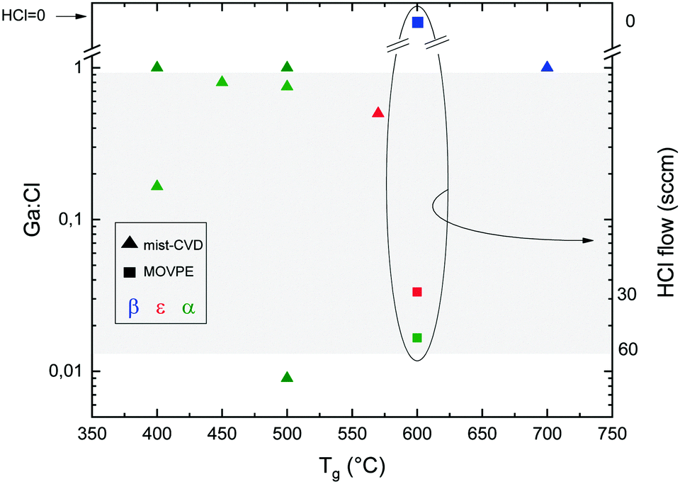 | ||
| Fig. 1 Ga2O3 phase on c-plane sapphire substrates as a function of the Ga:Cl ratio and temperature for the MOVPE (squares) and mist-CVD (triangles) techniques. Red symbols: ε-Ga2O3. Blue symbols: β-Ga2O3. Green symbols: α-Ga2O3. In the circle are summarized the data from ref. 42 using HCl along with O2 and TEG: for these points the HCl flow is reported on the right y axis. The grey area represents reasonable Ga:Cl ranges for HVPE growth. | ||
For HVPE it is more difficult to calculate the effective Ga:Cl ratio, because the reacting species (GaCl or GaCl3)29 are obtained by flowing HCl on liquid Ga and it is difficult to accurately estimate the yield of this reaction. Nevertheless, we can conceive that Ga:Cl is certainly less than 1. If one supposes that the yield of the reaction was 1, all the HCl would be converted either into GaCl or into GaCl3, with Ga:Cl = 1 or 1/3. If the yield was less than unity, there would still be some HCl present, again leading to Ga:Cl < 1. For this reason, in Fig. 1 only a reasonable range for Ga:Cl in HVPE is indicated in the grey area for comparison with the other techniques.
Since it is meaningless to plot arbitrary points from HVPE in Fig. 1, it is necessary to look for an additional parameter to compare some of the HVPE data found in the literature. Therefore, Fig. 2 reports the resulting Ga2O3 phase from samples grown by HVPE and MOVPE depending on the O2:HCl flow ratios as a function of the growth temperature. The values were obtained from ref. 26, 42, 53 and 54 and from private communications with their corresponding authors.
 | ||
| Fig. 2 Ga2O3 phase on c-plane sapphire substrates as a function of the O2:HCl ratio and growth temperature for HVPE-grown samples. Circles: HVPE growth. Squares: MOVPE growth. Red symbols: ε-Ga2O3. Blue symbols: β-Ga2O3. Green symbols: α-Ga2O3. | ||
While finding a trend between the Ga:Cl ratio and temperature is not straightforward, from Fig. 1 it can be noted that for mist-CVD Ga:Cl = 1 is the used condition, although the growth of the α polymorph is possible also with a lower Ga:Cl ratio. Mist-CVD is also more prone to provide α-Ga2O3 at lower temperatures. From Fig. 2 it is also evident that α-Ga2O3 is preferentially obtained by HVPE at lower temperatures, with the exception of the ε-phase obtained at 450 °C by Son et al.,54 and that the ε phase can be stabilized on sapphire by increasing the O2:HCl ratio both by MOVPE and HVPE at a particular temperature.42,53 Higher temperatures favour the β phase, as it happens for mist-CVD.50
Chlorine seems to play an important role in the stabilization of different Ga2O3 polymorphs. A secondary ion mass spectroscopy (SIMS) investigation on different Ga2O3 layers53 evidenced a higher amount of Cl incorporated in the ε-phase with respect to the α one (5 × 10¹⁷vs. 3 × 10¹⁵ atoms per cc, respectively); this happens despite the lower O2:HCl ratio employed to grow the α-Ga2O3 layer. Interestingly, in this work Cl seems to be confined at the Ga2O3/sapphire interface for the α phase layer (Fig. 3). However, because of the unknown value of the distribution coefficient of Cl in gallium oxide, it is not straightforward to relate a volumetric SIMS measurement to a surface concentration of Cl atoms, to understand if they may indeed change the surface energy of Al2O3. Density functional theory (DFT) models predict that at room temperature the saturation surface coverage of HCl on Al2O3 is approximately one adsorbed HCl molecule per five surface Al sites.55 A deeper understanding of the HCl-Al2O3 surface interaction at higher temperature may be useful to clarify this point. It should also be noted that the presence of Cl at the outset of growth could be related to the formation of very stable Al–Cl bonds at the Al2O3(0001) surface with bond dissociation energy ΔHf = 495 J mol−1. This may change both the surface energy of the sapphire and the interfacial energy between the two oxides53 and it may be one factor – but not the only one – promoting the growth of the metastable ε or α phases.
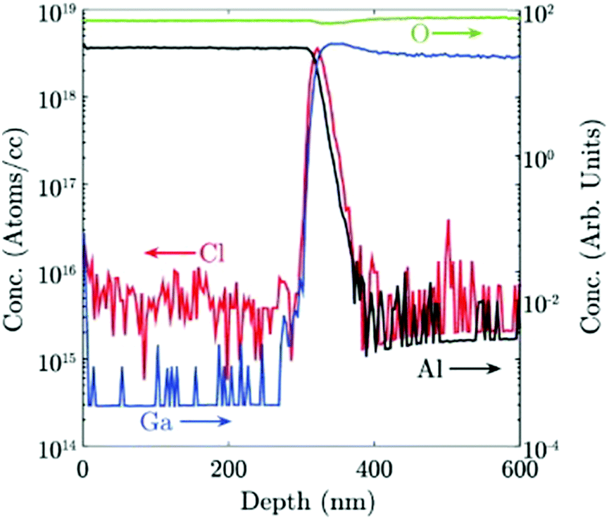 | ||
| Fig. 3 Cl concentration in atoms per cc and Ga, Al and O concentration in arbitrary units, measured by SIMS for an α-Ga2O3 sample grown by HVPE at 650 °C. Reproduced from ref. 53. | ||
Other authors report incorporation of Cl throughout the whole layer, with a concentration of about 5 × 10¹⁶ atoms per cc for α-Ga2O3 HVPE growth at 470 °C.54 Oshima et al.26 found higher hydrogen and chlorine concentration for ε-Ga2O3 grown on GaN(0001), AlN(0001), and β-Ga2O3(01) with respect to the one found in α-Ga2O3 grown on c-plane sapphire while maintaining the same synthesis conditions and in the same HVPE reactor (2 × 10¹⁸vs. 7 × 10¹⁶ atoms per cc for Cl and 1 × 10¹⁸vs. 4 × 10¹⁶ atoms per cc for H). In the same work it was observed that also H, resulting from HCl decomposition, is incorporated in the growing layer. As H is known to be a donor in Ga2O356,57 this is an important element to take into consideration for its electrical properties when the growth is performed under H-based carrier gases (H214 or HCl). It is also worth mentioning that the incorporation of Cl was reported with a concentration of about 1016 atoms per cc in β-Ga2O3 grown by HVPE at 800–1050 °C,58 indicating reasonably higher Cl desorption while increasing the deposition temperature.
For MOVPE, Sun et al.42 reported that the HCl flow does not affect the Cl concentration incorporated in the films regardless of the phase, speculating that HCl could just act as a catalyst for the growth.
Up to now, no study on the chemical details of the growth of Ga2O3 in the presence of HCl has been published; however, a theoretical study of the MOVPE growth of GaAs with HCl (without oxygen)59 concluded that the interaction of TEG and HCl results in the formation of a stable GaCl molecule in the gas phase. GaCl can be adsorbed on the growth surface up to a substrate temperature of 900 °C. On the other hand, the already mentioned AlCl termination expected at the sapphire substrate–Ga2O3 layer interface should be more energetically stable.
MOVPE growth of α- or ε-Ga2O3 is typically obtained with the use of trimethyl- or triethyl-gallium (TMG and TEG) and water or oxygen as an oxidizing agent. By gathering several sets of data on Ga2O3 MOVPE growth from ref. 9, 14, 42 and 60–64, and from the same studies but considering the Ga:H2O ratio (Fig. 1), it is possible to plot the relation between the growth temperature and the Ga:H2O or Ga:O2 ratio in the gas phase for the different growth methods (Fig. 4).
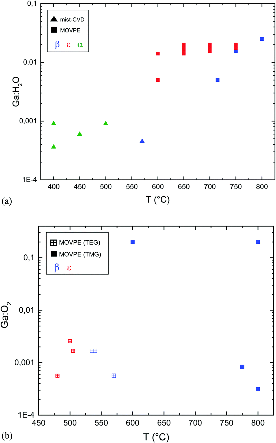 | ||
| Fig. 4 (a) Ga2O3 phase as a function of the growth temperature (Tg) and H2O:Ga ratio. All MOVPE points are from growth with H2O and TMG. (b) Ga2O3 phase as a function of the MOVPE growth temperature (Tg) and Ga:O2 ratio. All the growth processes are on c-plane sapphire substrates. Triangles: mist-CVD growth. Filled squares: MOVPE growth with trimethyl gallium. Crossed squares: MOVPE growth with triethyl gallium. Red symbols: ε-Ga2O3. Blue symbols: β-Ga2O3. Green symbols: α-Ga2O3. | ||
It should be noted that MOVPE growth with TEG and O2 at temperatures lower than 575 °C resulted in polycrystalline β-Ga2O3 layers.63
In MOVPE, the choice between TMG or TEG usually reflects a different growth rate and better accuracy in the gallium supply control, since TEG has a lower partial pressure with respect to TMG, allowing for easier control of lower gallium flow rates. It also produces lower carbon contamination (due to metalorganic decomposition) via β-hydride elimination rather than by a radical mechanism. TEG has lower stability compared to TMG and pyrolyses at significantly lower temperatures, thus allowing to grow higher purity layers at lower growth temperatures compared to TMG.65
Another consideration should be made regarding the use of H2O or O2; the chemistry of the two precursors is totally different, as discussed by Wagner et al. for the growth of β-Ga2O3 between 750 and 850 °C.9 When pure O2 is employed, the formation energy of oxygen vacancies is substantially increased, which in turn lowers their concentration. When H2O is employed, the oxygen partial pressure is considerably lower and oxygen vacancies are expected to form spontaneously.66 An additional mechanism can also take place: hydrogen may occupy oxygen vacancy sites by forming Ga–H species, thus reducing the surface state density. Therefore, the chemical potential of the surface will be more homogeneous and diffusion of desorbed atoms on the surface will be enhanced.9Fig. 5 shows the composition of the growth atmosphere for real growth conditions using the FactSage software package, as illustrated by Wagner et al.9 The main products of the reaction between TMG and pure oxygen are solid Ga2O3, gaseous oxygen, water, and carbon dioxide. If water is used as the oxygen source, H2 is present at high concentration, while O2 molecules are not present at all, because they are fully consumed by organic species. CO2 is also present, but at a concentration several orders of magnitude lower than H2. H2O dissociation and its chemisorption on the Ga2O3 surface can significantly influence the nature of the surface sites, which in turn affects the subsequent adsorption and surface mobility of other molecules. On the other hand, defects like oxygen vacancies (VO) can affect the surface chemistry of the Ga2O3 surface. H2O is preferably adsorbed in the form of molecules producing a hydrated Ga2O3 surface, while adsorbed CO2 is activated and results in the formation of carbonate species with a slightly endothermic reaction.67 In the framework of this reaction the presence of VO on the Ga2O3 surface plays an important role since (i) CO2 tends to occupy them, while (ii) H2O spontaneously dissociates at the oxygen vacancy side.
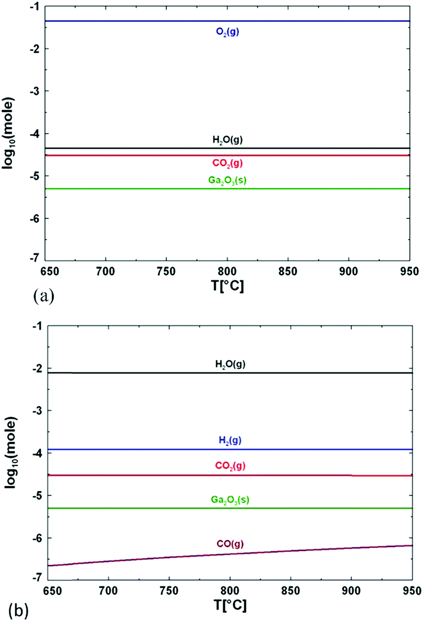 | ||
| Fig. 5 Calculated concentration of the main species formed during growth of Ga2O3 layers when using (a) oxygen and (b) water as an oxygen source. Reproduced with permission from ref. 9. | ||
Therefore, the choice of the precursor (i.e., H2O or O2) can directly affect the concentration of oxygen vacancies in the deposited Ga2O3 layers. This is an important information, since it has been reported that the VO concentration is related to the performances of β-Ga2O3 photodetectors; in particular, reducing the VO concentration enhances the carrier drift and recombination, resulting in a higher photodetector response speed and higher photo/dark current ratio.68,69 If the use of H2O leads to a different density of oxygen vacancy sites9 for the growth of β-Ga2O3, a comparison of the electrical properties of samples grown by mist-CVD and MOVPE with very different H2O content may give some hints in the understanding of the growth mechanisms.
On the other hand, the use of O2 or H2O leads to completely different results with MOVPE in a wide temperature range (square symbols in Fig. 4a and b). In particular, β-Ga2O3 grown at temperatures lower than 575 °C with TEG and O2 is polycrystalline, while single crystalline layers are obtained with TMG and O2 only at Tg higher than 600 °C. The ε phase is stabilized with the use of H2O in a wide range of temperatures between 600 and 750 °C. Nonetheless, β-Ga2O3 can also be grown using H2O at higher Tg by properly tuning the growth conditions, and ε-Ga2O3 can be obtained at lower temperatures by using O2 instead of H2O. To the best of the authors’ knowledge, no literature studies have been yet focused on the possibility to obtain different VO concentrations in orthorombic ε layers deposited with H2O or O2 and their possible role in photodetector performances.
From Fig. 4(a) and (b) it is evident that the use of H2O in the gas phase instead of gaseous O2 changes the MOVPE growth process and favours the growth of ε-Ga2O3. Very significant are the results obtained by Sun et al.42 (not reported in the graph): using O2 and TEG as reagents they obtained β-Ga2O3 at 600 °C, but when 30 sccm of HCl was added to the gas phase, it stabilised ε-Ga2O3. When the HCl flow was further increased up to 60 sccm, layers of the α phase were obtained. These results confirm the important role of HCl in the stabilization of different Ga2O3 crystal phases. As the use of H2O instead of O2 in MOVPE definitely promotes the growth of ε-Ga2O3 over β-Ga2O3, one may speculate that hydrogen, alongside HCl, has also a role in stabilizing the ε phase. This does not clash with the results by Sun et al.;42 on the contrary, it would suggest that both H and Cl are active factors in stabilizing the growth of ε-Ga2O3. However, since pushing more HCl flow in MOVPE promotes the growth of the α phase, it is not clear why the same does not happen with high H2O flow at similar Tg; there have been no studies reporting on the MOVPE growth of α-Ga2O3 with the use of H2O or O2 without the addition of HCl (which seems to be essential to dissolve GaCl). Nonetheless, α-Ga2O3 was obtained at T > 760 °C on sapphire using TMG, and N2O as an oxidizing agent, and adding boron or nitrogen in the lattice (with triethylboron and dimethylhydrazine) to adjust the mismatch;70 three monolayers of α-Ga2O3 were always observed at the interface with sapphire before the growth of β-Ga2O3 at 800 °C using TMG and H2O.60
Sun et al.42 reported DFT calculations with the relative energy difference for the formation of different polymorphs between pure Ga2O3 and hydrogenated gallium oxide, due to the introduction of H in the gas phase with HCl (Table 3). These DFT calculations considered the deposition of Ga2O3 at 600 °C in a MOVPE reactor with O2, TEG and HCl as precursors.
| α | ε | β | |
|---|---|---|---|
| Ga2O3 | 0.15 | 0.04 | 0.00 |
| Ga4O6H | 0.07 | 0.00 | 0.02 |
| Ga4O6H2 | 0.01 | 0.00 | 0.03 |
From Table 3 we notice that without H in the gas phase (reflecting the absence of H in the lattice), the β phase has the lowest formation energy in agreement with the experimental data previously discussed. Therefore, H may act as a catalyst for the stabilization of metastable phases, i.e., modifying the relative energy difference between the β phase and the other polymorphs and allowing, for instance, the deposition of ε layers at a Tg of 600 °C. Sun et al.42 suggested also that further studies regarding kinetic models may be required in order to understand the mechanism behind the crystallization process in the presence of HCl in order to: (1) fully understand the growth rate dependence on the HCl flow rates of Ga2O3 with the same phase, (2) consider the oversupply of HCl gas into the chamber to check the phases and growth rate, and (3) replace HCl with another gas to conduct similar studies, since increasing the HCl flow beyond a threshold results in the crystallization of α-Ga2O3. It is noteworthy that also Mist-CVD and HVPE show a similar tendency to obtain the α or ε phase at the growth temperatures reported by Sun et al.42 due to the presence of H2O and HCl in the gas phase.
In the case of physical vapour deposition (PVD) techniques like PLD and MBE it is not correct to talk about precursors since usually the only elements involved in the deposition process are the ones constituting the deposited layer (excluding the unavoidable presence of impurities), i.e., gallium and oxygen in the case of Ga2O3 growth. PVD heteroepitaxy of Ga2O3 on c-plane sapphire substrates mostly results in the formation of (01)-oriented monoclinic layers with six rotational domains.71–74 Nonetheless, a thin (≈1 nm) α-Ga2O3 interlayer can be usually identified at the substrate/β-Ga2O3 layer interface for both MBE and PLD films.60
Particularly, for MBE the growth window for (01) β-Ga2O3 heteroepitaxial layers on c-plane sapphire is limited to relatively low substrate temperatures (Tg ≈ 500–600 °C) and/or high oxygen-to-gallium flux ratios75 due to the high volatility of the Ga2O suboxide which is formed on the substrate surface as a first step of its peculiar growth kinetics.76 Outside of this growth window and with the employment of just Ga- and O-fluxes, no Ga2O3 layer can be deposited with MBE in either of its polymorphs on c-plane sapphire substrates. Notably, the stabilization of the orthorhombic ε-polymorph of Ga2O3 with PVD techniques like MBE and PLD specifically requires the introduction of a catalyst element during growth, i.e., In43 or Sn;44 the supply of an In- or a Sn-flux together with Ga and the activated oxygen (provided via an oxygen plasma source) helps to widen the narrow deposition window of Ga2O3 on c-plane sapphire to both (i) higher deposition temperatures (e.g., Tg = 700 °C) and (ii) lower oxygen-to-metal flux ratios. In particular, the deposition of phase-pure ε-Ga2O3 layers is limited to growth conditions that do not allow for any β-Ga2O3 formation (Fig. 6).44 Under these synthesis conditions the catalyzing element is not incorporated to a large extent inside the deposited layer. The presence of a (01) β-Ga2O3 nucleation layer at the c-plane sapphire/ ε-Ga2O3 interface is usually reported.43,44,77 As in the case of other growth techniques previously discussed in this article, also the PVD deposited ε-Ga2O3 layers on c-plane sapphire substrates are characterized by the presence of the same rotational domains giving rise to an (001)-oriented columnar structure.43,44,70
 | ||
| Fig. 6 Comparison of the growth rates as a function of the Ga-flux (expressed as beam equivalent pressure, BEP) during heteroepitaxial growth of Ga2O3 on c-plane sapphire substrates with and without the employment of an additional Sn flux (red triangles and black squares, respectively) via plasma-assisted MBE. The oxygen flow is kept constant at 0.5 standard cubic centimetres per minute with an oxygen plasma power of 150 W. Graph reproduced with permission from ref. 44. | ||
The reasons behind the stabilization of the ε phase during PVD growth of Ga2O3 are not fully understood yet. That is why it is worth briefly describing this peculiar growth mechanism based on the collaborative effect of kinetics and thermodynamics, i.e., metal-exchange catalysis (an extensive growth mechanism description is discussed in ref. 43, 44 and 78). The catalyzing element (i.e., In and Sn) is (i) characterized by a higher oxidation efficiency with respect to Ga and, even though its growth kinetics (i.e., In2O3 and SnO2) is based on a similar 2-step process,75,76 (ii) its volatile suboxide (i.e., In2O and SnO) which is initially formed and adsorbed on the substrate surface has a lower vapor pressure with respect to the Ga2O suboxide. As a matter of fact, both In2O3 and SnO2 can be grown in plasma-assisted MBE at higher temperatures and with relatively lower oxygen-to-metal flux ratios with respect to Ga2O3.43,75,76 Therefore, due to its kinetic advantage, the adsorbed suboxide of the catalyst element can be further oxidized to its solid oxide form on the substrate surface (i.e., In2O3 and SnO2). At this stage of the growth process, Ga is replacing the catalyst element (thermodynamic advantage of Ga over In and Sn), which can be either desorbed or re-utilized in the framework of an installed catalytic cycle. In both cases, under these conditions the catalytic cycle results in very limited incorporation of the catalyst element inside the deposited Ga2O3 layer.43,44 This is true even in the presence of large catalyst fluxes (e.g., In = 1/3 of the Ga-flux).43 In other words, in metal-exchange catalysis the catalyst element works as an oxygen getter/reservoir for Ga2O3 growth, efficiently expanding its deposition window. ε-Ga2O3 layers in the presence of the catalysing element Sn were also reported for PLD grown thin films on MgO(111), SrTiO3(111), and yttria-stabilized ZrO2(111) substrates.70,79 Notably, MBE In-mediated metal-exchange catalysis has been also applied to widen the growth window of Ga2O3 layers deposited on all the available β-Ga2O3 bulk substrate orientations [i.e., (010), (100), (001), and (01)]12,13,80 but differently from the discussed heteroepitaxial growth; in this case the deposited layers always preserved the monoclinic structure of the substrate.
2.2. Temperature
From Fig. 1, 2 and 4 it is evident that the growth temperature Tg plays a critical role in tailoring the crystal phases of Ga2O3. In particular for CVD growth, high temperatures are usually necessary for the crystallization of the thermodynamically stable β-Ga2O3 polymorph (regardless of the deposition techniques, precursors, and gas phase composition). However, the monoclinic phase has been already reviewed in depth in the literature1,40 and, therefore, we will not include a discussion on β in this review. Generally, at Tg between 400 and 700 °C the driving force for the crystallization of one particular phase can be found in the kinetics of the reactions and/or in the growth process itself; for example, by simply changing the precursor from H2O to O2 the Ga2O3 switches from ε to β (see Section 2.1).The growth temperature is a key factor in controlling α or ε phase stabilization by mist-CVD growth; in particular, Tg ≤ 500 °C favours the deposition of α-Ga2O3 layers, while higher temperatures (up to Tg < 700 °C) result in the synthesis of ε-Ga2O3 films (Fig. 1).
With HVPE (Fig. 2) it is generally easier to crystallize the α phase in a wider temperature range compared to the mist-CVD one. ε-Ga2O3 could be obtained by HVPE at similar temperatures to mist-CVD (Tg = 650 °C) by appropriately tuning the gas phase composition, with the exception of one article54 that reports the nucleation of an ε-Ga2O3 layer at a Tg of 450 °C.
Another interesting observation (Fig. 4) is that α-Ga2O3 is obtained by mist-CVD in a temperature range (400–550 °C) lower than the one typically used in MOVPE; one hypothesis may be related to the different kinetics of the reactions, due to the different precursors used. While in mist-CVD Ga3+ ions should be directly present in the gas phase so that no precursor decomposition has to occur, in MOVPE processes TMG (or TEG) may not have sufficient energy to form Ga2O3, and may tend to react directly with H2O in the vapour phase without leading to Ga2O3 crystallization. Low MOVPE deposition temperatures (550 °C) result in polycrystalline Ga2O3 using H2O and TMG. In this framework, it is worth noting that by using an ALD process instead of a standard MOVPE growth regime, crystalline ε-Ga2O3 could be obtained also at 550 °C;14 while the decomposition of the gallium precursor may have an important role in the growth process, the parasitic reactions in the gas phase between the metal–organic precursor and water may also play a role at lower temperatures. The use of water and TEG instead of TMG could be a possible route to obtain α-Ga2O3 by MOVPE at Tg comparable with mist-CVD without the use of Cl, as TEG has a lower decomposition temperature and prevents pre-reactions between Ga and water.65 However, Chen et al.64 reported the deposition of an ε-Ga2O3 layer at 500 °C by using O2 and TEG at 35 mbar. For this reason, it seems that the use of a particular Ga precursor is not sufficient to explain why mist-CVD at lower temperatures results in α-Ga2O3; other factors, such as the amount of H2O (or H) or the growth pressure may also play a role in this process. A possible explanation may be that, by changing the growth temperature, the relative energy differences between the phases reported in the presence of H (Table 3) may assume different values, with the α phase more favoured than the ε one. Theoretical calculations and DFT models may help in understanding these aspects.
In the case of PVD deposition techniques, both PLD and MBE independently showed that the stabilization of the ε phase over the β one is associated with the employment of higher growth temperatures (Tg ≥ 465 °C in PLD73 and Tg = 550–700 °C in MBE43,44) during the In/Sn-mediated deposition process. In the case of α-Ga2O3 the deposition temperature with MBE (no catalyst employed) has been so far limited to 500 °C ≤ Tg ≤ 640 °C.81–83
2.3. Growth rate
HVPE, MOVPE and mist-CVD all allow for comparable Ga2O3 growth rates of about 500–1000 nm h−1. Nonetheless, HVPE can also reach growth rates of about 10 μm h−1 by increasing the flow rates.53 If comparable synthesis parameters and similar growth rates are considered, the stabilization of different Ga2O3 polymorphs should be discussed in light of the chemical reactions triggered by the different employed precursors (Section 2.1).Generally, the growth rate can be related to the available time for lattice arrangement during Ga2O3 nucleation. In particular, a faster growth rate, typical of HVPE, may not allow the adatoms to rearrange on the layer/substrate surface, therefore not permitting the formation of the thermodynamically stable β-phase. In the case of heteroepitaxial growth on c-plane sapphire, the diffusing adatoms initially bonded to the oxygen and aluminium sites of the (0001) substrate surface are preferably ordering as α-Ga2O3 and are unable to undergo rearrangement to the β-Ga2O3 or ε-Ga2O3 phase before the next impinging atoms are adsorbed on the previously formed corundum surface; each layer of α-Ga2O3 is then constrained or buried by the rapidly depositing subsequent layers.53 In this situation also the substrate crystallography, the eventual presence of a nucleation layer, and therefore the resulting lattice mismatch play an important role in the stabilization of the Ga2O3 phase (see Section 2.4).
The role of the growth rate in stabilizing the Ga2O3 phase is evidenced also by comparing the studies of Dang et al. and Kim et al.,45,84 where mist-CVD growth at the same Tg of 400 °C results in the stabilization of different Ga2O3 phases as a function of different growth rates. In particular, a higher growth rate of about 860 nm h−1 resulted in the deposition of a phase-pure α-Ga2O3 layer,45 while a lower growth rate of 260 nm h−1 ended up in the synthesis of a mixed α and β phase sample as observed by bandgap measurements.84 This supports the idea that the time given to the adatoms to rearrange on the layer surface, i.e., before the atoms necessary to cover the next monolayer are adsorbed, may influence the stabilization of a particular phase.
A similar picture can be also valid for MBE growth, since the deposition of ε-Ga2O3 layers is associated with a higher growth rate with respect to the β ones (Fig. 6) under similar synthesis conditions (i.e., Tg ≈ 700 °C and a low oxygen-to-metal flux ratio).43,44 Usually the full incorporation of the impinging Ga-flux can be obtained in such a regime, with maximum growth rates in the range of 100 to 300 nm h−1. Nonetheless, it should be considered that the peculiar growth process associated with the stabilization of the ε-phase (metal exchange catalysis) specifically requires the employment of synthesis conditions where Ga2O3 would hardly grow without a catalyst (see Section 2.1). In fact, similar growth rates, characterized by full Ga-flux incorporation, could be obtained at lower growth temperatures and high O-flows in the case of β-Ga2O3 layers.
2.4. Substrate and lattice match
While in the previous paragraphs we mainly considered c-plane sapphire as the reference substrate to compare different growth methods, in this section we will discuss the influence of a different substrate and/or of a buffer layer.The growth of ε-Ga2O3 has been demonstrated on various substrates such as gadolinium gallium garnet (GGG) (cubic), MgO(111), yttria-stabilized ZrO2 (YSZ)(111), α-(AlxGa1−x)2O3(0001), NiO(111), AlN, and GaN.26,28,85,86 The synthesis conditions that allow for a particular Ga2O3 polymorph strongly depend on the crystallographic mismatch between the substrate and epilayer as well as the surface crystal structure.
Some authors have reported that substrates of a cubic material (MgO and YSZ) oriented along the (111) direction allow one to obtain single phase (001)-oriented ε-Ga2O3 layers by mist-CVD in a wide range of deposition temperatures (400–700 °C) where typically α-Ga2O3 is obtained on c-plane sapphire.86,87 On the other hand, the growth on c-sapphire proved to be more difficult, as mixed phases are obtained in standard growth conditions by Mist-CVD, either α–ε at low temperatures or ε–β at high temperatures, due to the crystal structure of α-Al2O3. It is noteworthy that the addition of a small buffer layer of NiO(111) on the sapphire substrate permits one to switch from α-Ga2O3 to ε-Ga2O3 growth in the whole 400–800 °C range.50
A lower mismatch between the substrate and the ε-Ga2O3 epilayer also appears to facilitate the growth of this phase; with the same HVPE growth conditions that resulted in α-Ga2O3 layers on c-plane sapphire substrates, (001)-oriented ε-Ga2O3 was obtained on GaN(0001), AlN(0001), and β-Ga2O3(01), the latter exhibiting superior crystal quality.29,88–90 A similar trend has been reported for Mist-CVD growth, where the use of MgO(111) instead of YSZ(111) substrates (with 2.5 and 20% nominal mismatch with ε-Ga2O3, respectively) allowed one to obtain single-phase (001)-oriented ε layers at much lower temperatures.86
However, a quantitative comparison of literature results based on the reported mismatch could be misleading, as the nominal lattice constant of the substrate might not be the parameter determining the effective mismatch. Furthermore, one should consider thermal mismatch, which leads to different lattice parameters for the substrate and epilayer at different temperatures. Indeed, as discussed in the introduction, epitaxial (001) ε-Ga2O3 grows by the formation of rotational domains, effectively altering the difference in lattice spacing between the epilayer and substrate. The most obvious example is the case of c-plane sapphire, where the nominal mismatch between α-Al2O3 and (001) ε-Ga2O3 is 65%, but by the effect of 120° lattice rotations the real mismatch is 4.8%.15 In this regard, it is interesting to mention that in spite of various tested substrates (and different crystal orientations), so far just (001)-oriented ε-Ga2O3 layers were reported in the literature. As mentioned, when proper structural characterization is given, all these samples are reported to be characterized by the presence of rotational domains resulting in columnar-like growth. Even if no dangling bonds are expected at the walls of the ε domains (differently from the case of rotational domains in β layers),91 it should be considered that their presence could result in a barrier for in-plane electronic conduction. There can be two effective strategies for growing pure ε-Ga2O3 single crystal layers, i.e., free of rotational domains: first, finding a properly matched substrate so to allow the accommodation of the orthorhombic structure of Ga2O3 in different crystal orientations [e.g., (010)] or, second, employing a proper in-plane substrate offcut, i.e., inducing the formation of properly spaced terraces whose kinks act as properly spaced nucleation sites (as already demonstrated for the growth of β layers on c-plane sapphire).92
As discussed in the previous section, heteroepitaxy of ε-Ga2O3 and α-Ga2O3 on sapphire may be favoured over the growth of β-Ga2O3 at lower temperatures due to reduced kinetical effects, allowing for the growth of a phase that is better lattice-matched to the substrate. In MOVPE, the growth on α-Al2O3 oriented along (1120), (1010), and (0112) allows for the growth of α-Ga2O370 at 700 °C using TEG and NO2 as an oxidizing agent.
ε-Ga2O3 was obtained by mist-CVD on an α-(Al0.4Ga0.6)2O3 buffer at temperatures lower than 600 °C, while the α phase was observed at higher temperatures, conceivably due to the lower lattice mismatch of 1.2% for the ε phase and 2.2% for the α phase. This effect was interpreted as due to a stepped surface: if the diffusion of adatoms is sufficiently high to reach step edges, the epitaxial layer grows with the α crystal structure of the buffer; if the growth temperature is not high enough, the lower-mismatch ε-Ga2O3 is favoured.48 Therefore, not only the substrate and its intrinsic mismatch with the relative polymorph lattice of the growing Ga2O3 layer should be considered as a growth parameter, but also its in-plane offcut and the associated terrace length. In this regard, the possible role of anisotropic diffusion lengths of the adsorbed species along different in-plane directions should also be considered, meaning that also the in-plane direction of the substrate offcut should be taken into account (i.e., both the terrace length and diffusion length along the offcut direction determine if the adsorbed species are able to reach the step edges and thus allow a step-flow growth mechanism), as already evidenced for β-Ga2O3.93
The indication that the α phase stabilization could be mainly driven by the mismatch with the underlying substrate lattice is also suggested by the MBE literature. In particular, corundum gallium oxide shares the same crystalline structure as sapphire and, therefore, it can in principle allow the growth of α-Ga2O3 along different sapphire orientations. In this case, the substrate–layer mismatch affects the maximum thickness that can be obtained: for c-plane sapphire (4.6% mismatch) only about a nanometer of α-Ga2O3 is achievable, while for a-plane sapphire layers of up to 10 nm were grown (3.4% mismatch).81 Nonetheless, the deposition of a Nd-doped α-Ga2O3 layer as thick as 100 nm has also been reported,83 suggesting that the presence of a dopant could affect the critical thickness of the layer on this orientation. Nonetheless, the thickest α-Ga2O3 films were obtained on r-plane sapphire:82 in this case a phase change to β-Ga2O3 was recorded after about 200 nm of α-Ga2O3, due to the formation of large exposed c-facets which favour subsequent monoclinic phase nucleation. Being the formation of facets also related to the chemical potential during the thin film deposition,94 we can argue that in the case of α-Ga2O3 layers on r-plane sapphire substrates the thickness limitation for the obtainment of phase-pure layers could be overcome by properly tuning the Ga-to-O flux ratio.
However, in the case of ε-Ga2O3 layers obtained via PVD techniques like MBE and PLD, the role of the substrate and the relative mismatch with the layer is less clear; there have been reports of layers grown on c-plane sapphire via MBE43,44 and PLD,73 while growth on substrates with a cubic structure [MgO(111), SrTiO3(111), and YSZ(111)] has just been reported for PLD.79 A buffer layer of β-Ga2O3 between c-sapphire and ε-Ga2O3 is usually present and evidenced by XRD and TEM. This could be an indication that an interlayer could be needed in order to accommodate the substrate–layer strain. The presence of a β-Ga2O3 buffer layer was observed also in the recent reports of ε-Ga2O3 layers on ITO/YSZ(111)87 and of van der Waals epitaxy of ε-Ga2O3 on synthetic mica,95 both via mist-CVD. In particular, the van der Waals epitaxy report of ε-Ga2O3 might hint at the fact that, in conditions with very weak chemical bonding between the substrate and epilayer, the growth of an initial layer of the most thermodynamically stable material in the β phase is needed, before obtaining epitaxial ε-Ga2O3. Moreover, the presence of an α-Ga2O3 buffer layer prior to ε-Ga2O3 deposition on c-plane sapphire has been reported for HVPE with the presence of Cl and interpreted to be related to semi-coherent growth of the α-phase, followed by ε-phase island nucleation and growth.53 Nonetheless, for both MBE and PLD where ε-Ga2O3 can be just obtained by In or Sn-mediated catalysed growth (see 2.1), also the crystal structure of the respective catalyst oxides (In2O3 or SnO2) – i.e., their oxygen atom distribution/coordination on the sample surface – could be at least partially responsible for the orthorhombic phase stabilization.
Moreover, it is worth mentioning that In-mediated MBE growth on (01) β-Ga2O3 single crystalline substrates under growth conditions that would otherwise allow for the synthesis of ε layers on c-plane sapphire substrates results in the preservation of the underlying substrate monoclinic structure.12,13 This is surprising considering that (i) the growth of ε-Ga2O3 on c-plane sapphire substrates is usually happening on top of (01) β-Ga2O3 interlayers, and (ii) the deposition of ε-Ga2O3 layers has been already previously reported on top of β-Ga2O3 bulk substrates via HVPE.26 One possible explanation relies on the formation of wide facets [i.e., different surfaces not parallel to the (01) one] during MBE (01)-homoepitaxy,12,13 which could favour the stabilization of the monoclinic polymorph, similarly to what has been previously discussed in the case of α-Ga2O3 on r-plane sapphire substrates.82
An interesting contribution about the role of the substrate in the nucleation of the α or ε phase is given in ref. 90 and 96, using HVPE to grow Ga2O3 on column-patterned sapphire. While the standard deposition on bare c-plane sapphire results in α-Ga2O3 with good crystallinity, the film on patterned substrates gives a mixture of α and ε-Ga2O3, with α-Ga2O3 vertical columns originating from the cones on the sapphire substrate, protruding up to the surface and capped with an irregular shape faceted pyramid on top. The ε-phase was located between these columns and had poorer crystallinity.
2.5. Pressure
Considering different deposition techniques that work in totally different pressure regimes (CVD vs. PVD) and with different oxidizing agents, a unified view towards the effect of pressure on the stabilization of Ga2O3 polymorphs is challenging. Nonetheless, internal comparisons among different pressure regimes (i.e., oxygen partial pressures) in the framework of the same deposition techniques can allow one to critically discuss this point.As a starting point, a simple consideration would be that MOVPE processes are usually performed at pressures from some tens up to some hundreds of mbar, while mist-CVD and HVPE generally use atmospheric pressure. As discussed above, by considering Fig. 1 and 2 it can be noticed that α-Ga2O3 is obtained by both HVPE and mist-CVD at low temperatures (up to 500–600 °C), while β or ε Ga2O3 is generally obtained in the same temperature range by MOVPE.
Regarding MOVPE with H2 and TEG, it was observed that a high pressure regime (>100 mbar) favours the nucleation of β-Ga2O3 in the gas phase, resulting in films with a mosaic surface, while ε-Ga2O3 is obtained at lower pressures, as already discussed in Section 2.3.64
For PLD, a flux of molecular oxygen is employed for the growth of oxide layers; for Sn-mediated growth of Ga2O3 it has been shown that the stabilization of the ε phase over the β one requires lower oxygen fluxes (pO2 ≤ 1 × 10⁻² mbar).79 For MBE growth it is complicated to discuss absolute oxygen partial pressure values; in fact, as this deposition technique must work at significantly lower pressure regimes during deposition processes (≤10−5 mbar), it therefore requires a flow of highly reactive oxygen so to allow for oxide layer deposition. This can be obtained either by an O-plasma source or by ozone, whose efficiencies are strongly dependent on every single experimental apparatus (e.g., distance of the sources from the substrate, purity of the provided ozone flux, efficiency of the O-plasma source). As already mentioned in Section 2.1, and consistently with the discussed PLD data, the stabilization via MBE of the ε phase over the β one requires lower oxygen-to-metal flux ratios.44 In both PLD and MBE, growing phase-pure ε-layers through metal-exchange catalysis (see Section 2.1) not only requires the presence of the catalyst element during growth, but also the employment of synthesis conditions that would not otherwise allow for β-Ga2O3 deposition (i.e., substrate temperatures >550 °C coupled with low oxygen fluxes). Otherwise, the competition between the normal growth regime (i.e., without a catalyst) and the catalysed one would result in mixed β–ε phase formation (see Fig. 6).44 Moreover, higher oxygen-to-metal flux ratios in MBE growth lead to remarkable incorporation of the catalyst element in the Ga2O3 layer, even though it is not clear if the incorporation can also be affected by the actual crystalline phase (i.e., ε or β).12,97
Differently from the ε-phase, the stability of α-Ga2O3 layers is apparently only weakly affected by different oxygen-to-metal flux ratios, as shown for heteroepitaxial growth by MBE on r-plane sapphire substrates.82
3. Conclusions
In this work we critically discussed the main aspects that rule the stabilization of different Ga2O3 polymorphs during growth. We considered and discussed all the main chemical and physical vapour phase deposition techniques and identified that the use of different precursors/catalysts (2.1), the deposition temperature (2.2), the growth rate (2.3), the substrate/nucleation layer (2.4), and the partial pressure of the processes (2.5) are all key parameters to be carefully considered for the synthesis of β, α, or ε Ga2O3 thin films. Naturally, it is very complicated to disentangle the effect of one single variable, but we were nevertheless able to highlight and critically examine several chemical/physical reasons behind different observations reported in the vast literature on Ga2O3 growth.In particular, we can here briefly summarize guidelines for the stabilization of different Ga2O3 polymorphs prepared by different deposition techniques (limited to growth on sapphire substrates for simplicity):
• Chemical vapour deposition techniques (HVPE, MOCVD, and Mist-CVD) on c-plane sapphire: β-Ga2O3 can be usually obtained at growth temperatures above 500 °C with O2 as a precursor, while at higher growth temperatures (Tg > 700 °C) it can be obtained also with H2O. ε-Ga2O3 can be grown (i) with an H2O precursor in a temperature window from 600 °C to 750 °C or (ii) if Cl is added at temperatures in the 600 °C range; however, the absolute Tg depends on the growth technique (e.g., MOVPE allows one to grow at lower Tg than MIST-CVD). α-Ga2O3 is generally grown at lower temperatures. In particular, MIST-CVD, which generally uses a high content of H2O precursor, allows for lower growth temperatures (400–550 °C) than MOVPE (600 °C); in HVPE, which makes use of O2, the addition of Cl favours the stabilization of this phase at temperatures up to 650 °C.
• Physical vapour deposition techniques (MBE and PLD): referring to c-plane sapphire substrates, (01)-oriented β-Ga2O3 can be usually synthesized at low substrate temperatures (e.g., Tg ≤ 600 °C) and/or at high oxygen-to-metal flux ratios (oxygen-rich regime). Single phase (001)-oriented ε-Ga2O3 can be deposited under growth conditions where the β polymorph would not grow – i.e., higher substrate temperatures (600 °C ≤ Tg ≤ 700 °C) and lower oxygen-to-metal flux ratios (metal-rich regime) – through the employment of a catalyst element (In and Sn) provided during the deposition process. α-Ga2O3 layers can be obtained on c-plane sapphire substrates just with limited thickness (≈3 nm), while on a-plane and especially r-plane sapphire substrates single phase thicker films can be deposited (maintaining the substrate orientation); no catalyst element is needed, Tg can be in the range of 500 °C to 650 °C, and no limitations on the oxygen-to-metal flux ratio are reported.
From a fundamental point of view, some questions arise about the exact chemical mechanisms that result in the stabilization of the ε phase, in particular concerning the role of additional elements involved in the growth process such as Cl and H (for CVD techniques) and Sn and In (PVD techniques). Additional insight into these processes could allow one to expand the range of useful elements to stabilize ε-Ga2O3 and other metastable polymorphs.
The role of the growth kinetics in the stabilization of the phase is also an important topic, if one aims to optimize the synthesis conditions. Indeed, some results indicate that the growth rate might be an important parameter to control the nature of the polymorphs; with its higher growth rate, HVPE could be the most convenient solution to stabilize α-Ga2O3 in a wide range of temperatures.
Moreover, despite the different substrates adopted for Ga2O3 heteroepitaxy, just (001) oriented ε-Ga2O3 and (01) oriented β-Ga2O3 layers were so far deposited. For both polymorphs these particular growth orientations result in the formation of domains which lead, in the case of β, to the formation of dangling bonds at the domain interfaces, while, in the case of ε, even without dangling bonds there could be negative effects on the transport properties of the layers. The use of different substrates and/or of proper offcuts could allow one to investigate this issue.
The identification of a well-defined growth window (e.g., oxygen- or metal-rich) and the employment of different precursors or catalysts for any particular polymorph can generate different point defects during growth, with a possible great impact on electronic devices (e.g., higher photodetector response speed and higher photo/dark current ratio).
As a final remark, we believe that particular effort should be made in the direction of the clear determination of the physical properties of the α and ε polymorphs, from both a theoretical and experimental point of view.
Therefore, we believe that this work could represent a landmark for the synthesis of different Ga2O3 polymorphs, which could help to unveil the full potential of this material for future applications.
Conflicts of interest
There are no conflicts to declare.Acknowledgements
This review summarizes the experience of about five years of research on MOVPE growth of Ga2O3, particularly of the ε polymorph, as well as the study of the literature relevant to different epitaxial technologies. We wish to thank many people at Parma University who contributed at different stages of the Ga2O3 research: A. Baraldi, A. Bosio, A. Parisini, M. Pavesi and R. Vantaggio from the SMFI Dept. – Physics Unit; G. Calestani and F. Mezzadri, from the SCVSA Dept. – Chemistry Unit, and the PhD students F. Boschi, C. Borelli, and V. Montedoro. The authors are also grateful to Dae-Woo Jeon, Haiding Sun and Usman Ul Muazzam for sharing useful information about their growth process and to G. Attolini of IMEM-CNR for useful discussion. This paper was written during the lockdown for the COVID-19 pandemic in Italy.References
- Gallium Oxide: Technology, Devices and Application, ed. S. Pearton, F. Ren and M. Mastro, Elsevier, 2018, ISBN: 9780128145210 (ebook), ISBN: 9780128145227 (Imprint) Search PubMed.
- R. Roy, V. G. Hill and E. F. Osborn, Polymorphism of Ga2O3 and the System Ga2O3–H2O, J. Am. Chem. Soc., 1952, 74, 719 CrossRef.
- H. Y. Playford, A. C. Hannon, E. R. Barney and R. I. Walton, Structures of Uncharacterised Polymorphs of Gallium Oxide from Total Neutron Diffraction, Chem. – Eur. J., 2013, 19, 2803–2813 CrossRef PubMed.
- M. Baldini, et al., Heteroepitaxy of Ga2(1−x)In2xO3 layers by MOVPE with two different oxygen sources, Cryst. Res. Technol., 2014, 49, 552–557 CrossRef CAS.
- S. Krishnamoorthy, et al., Modulation-doped β-(Al0.2Ga0.8)2O3/Ga2O3 field-effect transistor, Appl. Phys. Lett., 2017, 111, 023502 CrossRef.
- Z. Guo, et al., Anisotropic thermal conductivity in single crystal β-gallium oxide, Appl. Phys. Lett., 2015, 106, 111909 CrossRef.
- F. Ricci, et al., Theoretical and experimental investigation of optical absorption anisotropy in β-Ga2O3, J. Phys.: Condens. Matter, 2016, 28, 224005 CrossRef CAS PubMed.
- M. H. Wong, K. Sasaki, A. Kuramata, S. Yamakoshi and M. Higashiwaki, Electron channel mobility in silicon-doped Ga2O3 MOSFETs with a resistive buffer layer, Jpn. J. Appl. Phys., 2016, 55, 1202B9 CrossRef.
- G. Wagner, et al., Homoepitaxial growth of β-Ga2O3 layers by metal-organic vapor phase epitaxy, Phys. Status Solidi, 2014, 211, 27–33 CrossRef CAS.
- R. Schewski, et al., Evolution of planar defects during homoepitaxial growth of β-Ga2O3 layers on (100) substrates – a quantitative model, J. Appl. Phys., 2016, 120, 011107 CrossRef.
- K. Sasaki, et al., Device-Quality beta-Ga2O3 Epitaxial Films Fabricated by Ozone Molecular Beam Epitaxy, Appl. Phys. Express, 2012, 5, 035502 CrossRef.
- P. Mazzolini,
et al., Substrate-orientation dependence of β-Ga2O3 (100), (010), (001), and (01) homoepitaxy by indium-mediated metal-exchange catalyzed molecular beam epitaxy (MEXCAT-MBE), APL Mater., 2020, 8, 021104 CrossRef.
- A. Mauze, Y. Zhang, T. Itoh, F. Wu and J. S. Speck, Metal oxide catalyzed epitaxy (MOCATAXY) of β-Ga2O3 films in various orientations grown by plasma-assisted molecular beam epitaxy, APL Mater., 2020, 8, 021104 CrossRef.
- F. Boschi, et al., Hetero-epitaxy of ε-Ga2O3 layers by MOCVD and ALD, J. Cryst. Growth, 2016, 443, 25–30 CrossRef CAS.
- F. Mezzadri, et al., Crystal structure and ferroelectric properties of ε-Ga2O3 films grown on (0001)-sapphire, Inorg. Chem., 2016, 55, 031114 CrossRef PubMed.
- M. B. Maccioni and V. Fiorentini, Phase diagram and polarization of stable phases of (Ga1−xInx)2O3, Appl. Phys. Express, 2016, 9, 041102 CrossRef.
- S. B. Cho and R. Mishra, Epitaxial engineering of polar ε-Ga2O3 for tunable two-dimensional electron gas at the heterointerface, Appl. Phys. Lett., 2018, 112, 1–6 Search PubMed.
- S. Leone, et al., Epitaxial growth of GaN/Ga2O3 and Ga2O3/GaN heterostructures for novel high electron mobility transistors, J. Cryst. Growth, 2020, 534, 125511 CrossRef CAS.
- A. Hassa, et al., Solubility limit and material properties of a κ-(AlxGa1−x)2O3 thin film with a lateral cation gradient on (001)Al2O3 by tin-assisted PLD, APL Mater., 2020, 8, 0–6 CAS.
- H. Nishinaka, N. Miyauchi, D. Tahara, S. Morimoto and M. Yoshimoto, Incorporation of indium into ε-gallium oxide epitaxial thin films grown: Via mist chemical vapour deposition for bandgap engineering, CrystEngComm, 2018, 20, 1882–1888 RSC.
- P. Ranga, S. B. Cho, R. Mishra and S. Krishnamoorthy, Highly tunable, polarization-engineered two-dimensional electron gas in ε-AlGaO3/ε-Ga2O3 heterostructures, Appl. Phys. Express, 2020, 13, 061009 CrossRef.
- A. Parisini, et al., Si and Sn doping of ε-Ga2O3 layers, APL Mater., 2019, 7, 1509 CrossRef.
- M. Mulazzi, et al., The electronic structure of ε-Ga2O3, APL Mater., 2019, 7, 1–7 CrossRef.
- H. J. Von Bardeleben, J. L. Cantin, A. Parisini, A. Bosio and R. Fornari, Conduction mechanism and shallow donor properties in silicon-doped ε-Ga2O3 thin films: An electron paramagnetic resonance study, Phys. Rev. Mater., 2019, 3, 84601 CrossRef CAS.
- M. Pavesi, et al., ε-Ga2O3epilayers as a material for solar-blind UV photodetectors, Mater. Chem. Phys., 2018, 205, 502–507 CrossRef CAS.
- Y. Oshima, E. G. Víllora, Y. Matsushita, S. Yamamoto and K. Shimamura, Epitaxial growth of phase-pure ε-Ga2O3 by halide vapor phase epitaxy, J. Appl. Phys., 2015, 118, 5–10 CrossRef.
- I. Cora, et al., The real structure of ε-Ga2O3 and its relation to κ-phase, CrystEngComm, 2017, 19, 1509 RSC.
- H. Nishinaka, H. Komai, D. Tahara, Y. Arata and M. Yoshimoto, Microstructures and rotational domains in orthorhombic ε-Ga2O3 thin films, Jpn. J. Appl. Phys., 2018, 57, 115601 CrossRef.
- Y. Oshima, E. G. Víllora and K. Shimamura, Halide vapor phase epitaxy of twin-free α-Ga2O3 on sapphire (0001) substrates, Appl. Phys. Express, 2015, 8, 0–4 CAS.
- X. Chen, et al., Solar-Blind Photodetector with High Avalanche Gains and Bias-Tunable Detecting Functionality Based on Metastable Phase α-Ga2O3/ZnO Isotype Heterostructures, ACS Appl. Mater. Interfaces, 2017, 9, 36997 CrossRef CAS PubMed.
- M. Oda, et al., Schottky barrier diodes of corundum-structured gallium oxide showing on-resistance of 0.1 mOhm cm2 grown by MIST EPITAXY®, Appl. Phys. Express, 2016, 9, 021101 CrossRef.
- M. Higashiwaki, K. Sasaki, A. Kuramata, T. Masui and S. Yamakoshi, Gallium oxide (Ga2O3) metal-semiconductor field-effect transistors on single-crystal β-Ga2O3 (010) substrates, Appl. Phys. Lett., 2012, 100, 013504 CrossRef.
- J. Furthmüller and F. Bechstedt, Quasiparticle bands and spectra of Ga2O3 polymorphs, Phys. Rev. B: Condens. Matter Mater. Phys., 2016, 93, 1–16 CrossRef.
- H. He, et al., First-principles study of the structural, electronic, and optical properties of Ga2O3 in its monoclinic and hexagonal phases, Phys. Rev., 2006, 74, 195123 Search PubMed.
- H. Peelaers, J. B. Varley, J. S. Speck and C. G. Van De Walle, Structural and electronic properties of Ga2O3–Al2O3 alloys, Appl. Phys. Lett., 2018, 112, 242101 CrossRef.
- J. Zhang, J. Shi, D. C. Qi, L. Chen and K. H. L. Zhang, Recent progress on the electronic structure, defect, and doping properties of Ga2O3, APL Mater., 2020, 8, 020906 CrossRef.
- R. Fornari, et al., Thermal stability of ε-Ga2O3 polymorph, Acta Mater., 2017, 140, 411 CrossRef CAS.
- I. Cora, et al., In situ TEM study of κ → β and κ → γ phase transformations in Ga2O3, Acta Mater., 2020, 183, 216–227 CrossRef CAS.
- S. D. Lee, K. Akaiwa and S. Fujita, Thermal stability of single crystalline alpha gallium oxide films on sapphire substrates, Phys. Status Solidi C, 2013, 10, 1592 CrossRef CAS.
- Gallium Oxide Materials Properties, Crystal Growth, and Devices, ed. M. Higashiwaki and S. FujitaI, Springer Series in Materials Science, 2020 Search PubMed.
- M. A. Herman, W. Richter and H. Sitter, Epitaxy, Springer Berlin Heidelberg, 2004, vol. 62 Search PubMed.
- H. Sun, et al., HCl Flow-Induced Phase Change of α-, β-, and ε-Ga2O3 Films Grown by MOCVD, Cryst. Growth Des., 2018, 18, 2370–2376 CrossRef CAS.
- P. Vogt, O. Brandt, H. Riechert, J. Lähnemann and O. Bierwagen, Metal-Exchange Catalysis in the Growth of Sesquioxides: Towards Heterostructures of Transparent Oxide Semiconductors, Phys. Rev. Lett., 2017, 119, 6–10 CrossRef.
- M. Kracht, et al., Tin-Assisted Synthesis of ε-Ga2O3 by Molecular Beam Epitaxy, Phys. Rev. Appl., 2017, 8, 1–8 Search PubMed.
- G. T. Dang, T. Kawaharamura, M. Furuta and M. W. Allen, Mist-CVD Grown Sn-Doped α-Ga2O3 MESFETs, IEEE Trans. Electron Devices, 2015, 62, 3640–3644 CAS.
- S. Yusa, D. Oka and T. Fukumura, High-: κ dielectric ε-Ga2O3 stabilized in a transparent heteroepitaxial structure grown by mist CVD at atmospheric pressure, CrystEngComm, 2019, 22, 381–385 RSC.
- T. Ma, et al., Heteroepitaxial growth of thick α-Ga2O3 film on sapphire (0001) by MIST-CVD technique, J. Semicond., 2019, 40, 012804 CrossRef CAS.
- R. Jinno, T. Uchida, K. Kaneko and S. Fujita, Control of Crystal Structure of Ga2O3 on Sapphire Substrate by Introduction of α-(AlxGa1−x)2O3 Buffer Layer, Phys. Status Solidi B, 2018, 255, 3–7 CrossRef.
- T. Uchida, R. Jinno, S. Takemoto, K. Kaneko and S. Fujita, Evaluation of band alignment of α-Ga2O3/α-(AlxGa1−x)2O3 heterostructures by X-ray photoelectron spectroscopy, Jpn. J. Appl. Phys., 2018, 57, 6–9 Search PubMed.
- Y. Arata, H. Nishinaka, D. Tahara and M. Yoshimoto, Heteroepitaxial growth of single-phase ε-Ga2O3 thin films on c-plane sapphire by mist chemical vapor deposition using a NiO buffer layer, CrystEngComm, 2018, 20, 6236–6242 RSC.
- U. U. Muazzam, P. Chavan, S. Raghavan, R. Muralidharan and Di. N. Nath, Optical Properties of Mist CVD Grown α-Ga2O3, IEEE Photonics Technol. Lett., 2020, 32, 422–425 Search PubMed.
- K. Uno, Y. Yamasaki and I. Tanaka, Growth mechanisms of zinc oxide and zinc sulfide films by mist chemical vapor deposition, Appl. Phys. Express, 2017, 10, 015502 CrossRef.
- Y. Yao, et al., Growth and characterization of α -, β -, and ε-phases of Ga2O3 using MOCVD and HVPE techniques, Mater. Res. Lett., 2018, 6, 268–275 CrossRef CAS.
- H. Son and D. W. Jeon, Optimization of the growth temperature of α-Ga2O3 epilayers grown by halide vapor phase epitaxy, J. Alloys Compd., 2019, 773, 631–635 CrossRef CAS.
- S. Alavi, D. C. Sorescu and D. L. Thompson, Adsorption of HCl on single-crystal α-Al2O3(0001) surface: A DFT study, J. Phys. Chem. B, 2003, 107, 186–195 CrossRef CAS.
- M. J. Tadjer, et al., Theory and Characterization of Doping and Defects in β-Ga2O3, ECS J. Solid State Sci. Technol., 2019, 8, Q3187–Q3194 CrossRef.
- Y. Qin, M. Stavola, W. B. Fowler, P. Weiser and S. J. Pearton, Hydrogen Centers in β-Ga2O3: Infrared Spectroscopy and Density Functional Theory, ECS J. Solid State Sci. Technol., 2019, 8, Q3103–Q3110 CrossRef CAS.
- H. Murakami, et al., Homoepitaxial growth of β-Ga2O3 layers by halide vapor phase epitaxy, Appl. Phys. Express, 2015, 8, 3–7 Search PubMed.
- C. Cavallotti, I. Lengyel, M. Nemirovskaya and K. F. Jensen, A computational study of gas-phase and surface reactions in deposition and etching of GaAs and AlAs in the presence of HCl, J. Cryst. Growth, 2004, 268, 76 CrossRef CAS.
- R. Schewski, et al., Epitaxial stabilization of pseudomorphic α-Ga2O3 on sapphire (0001), Appl. Phys. Express, 2015, 8, 011101 CrossRef.
- S. H. Park, H. S. Lee, H. S. Ahn and M. Yang, Crystal Phase Control of ε-Ga2O3 Fabricated using by Metal-Organic Chemical Vapor Deposition, J. Korean Phys. Soc., 2019, 74, 502–507 CrossRef CAS.
- M. J. Tadjer, et al., Structural, Optical, and Electrical Characterization of Monoclinic β-Ga2O3 Grown by MOVPE on Sapphire Substrates, J. Electron. Mater., 2016, 45, 2031–2037 CrossRef CAS.
- Y. Zhuo, et al., β-Ga2O3 versus ε-Ga2O3: Control of the crystal phase composition of gallium oxide thin film prepared by metal-organic chemical vapor deposition, Appl. Surf. Sci., 2017, 420, 802–807 CrossRef CAS.
- Y. Chen, et al., Growth Pressure Controlled Nucleation Epitaxy of Pure Phase ε And β-Ga2O3 Films on Al2O3via Metal-Organic Chemical Vapor Deposition, Cryst. Growth Des., 2018, 18, 1147–1154 CrossRef CAS.
- C. Plass, H. Heinecke, O. Kayser, H. Lüth and P. Balk, A comparative study of Ga(CH3)3, Ga(C2H5)3 and Ga(C4H9)3 in the low pressure MOCVD of GaAs, J. Cryst. Growth, 1988, 88, 455–464 CrossRef CAS.
- Y. X. Pan, C. J. Liu, D. Mei and Q. Ge, Effects of hydration and oxygen vacancy on CO2 Adsorption and activation on β-Ga2O3(100), Langmuir, 2010, 26, 5551–5558 CrossRef CAS PubMed.
- Y. X. Pan, D. Mei, C. J. Liu and Q. Ge, Hydrogen adsorption on Ga2O3 surface: A combined experimental and computational study, J. Phys. Chem. C, 2011, 115, 10140–10146 CrossRef CAS.
- S. H. Lee, et al., Sub-microsecond response time deep-ultraviolet photodetectors using α-Ga2O3 thin films grown via low-temperature atomic layer deposition, J. Alloys Compd., 2019, 780, 400–407 CrossRef CAS.
- D. Guo, et al., Decrease of oxygen vacancy by Zn-doped for improving solar-blind photoelectric performance in β-Ga2O3 thin films, Electron. Mater. Lett., 2017, 13, 483–488 CrossRef CAS.
- V. Gottschalch, et al., Heteroepitaxial growth of α-, β-, γ- and κ-Ga2O3 phases by metalorganic vapor phase epitaxy, J. Cryst. Growth, 2019, 510, 76–84 CrossRef CAS.
- M.-Y. Tsai, O. Bierwagen, M. E. White and J. S. Speck, β-Ga2O3 growth by plasma-assisted molecular beam epitaxy, J. Vac. Sci. Technol., A, 2010, 28, 354–359 CrossRef CAS.
- E. G. Víllora, K. Shimamura, K. Kitamura and K. Aoki, Rf-plasma-assisted molecular-beam epitaxy of β-Ga2O3, Appl. Phys. Lett., 2006, 88, 031105 CrossRef.
- M. Orita, H. Hiramatsu, H. Ohta, M. Hirano and H. Hosono, Preparation of highly conductive, deep ultraviolet transparent β-Ga2O3 thin film at low deposition temperatures, Thin Solid Films, 2002, 411, 134–139 CrossRef CAS.
- S. Nakagomi and Y. Kokubun, Crystal orientation of β-Ga2O3 thin films formed on c-plane and a-plane sapphire substrate, J. Cryst. Growth, 2012, 349, 12–18 CrossRef CAS.
- P. Vogt and O. Bierwagen, The competing oxide and sub-oxide formation in metal-oxide molecular beam epitaxy, Appl. Phys. Lett., 2015, 106, 1–5 CrossRef.
- P. Vogt and O. Bierwagen, Quantitative subcompound-mediated reaction model for the molecular beam epitaxy of III–VI and IV–VI thin films: Applied to Ga2O3, In2O3, and SnO2, Phys. Rev. Mater., 2018, 2, 1–5 Search PubMed.
- Y. Cai, et al., Tin-assisted growth of ε-Ga2O3 film and the fabrication of photodetectors on sapphire substrate by PLD, Opt. Mater. Express, 2018, 8, 3506 CrossRef CAS.
- O. Bierwagen, P. Vogt and P. Mazzolini, Plasma-Assisted Molecular Beam Epitaxy 2, in Gallium Oxide: Materials Properties, Crystal Growth, and Devices, ed. M. Higashiwaki and S. Fujita, Springer International Publishing, 2020, pp. 95–121 DOI:10.1007/978-3-030-37153-1_6.
- M. Kneiß, et al., Tin-assisted heteroepitaxial PLD-growth of κ-Ga2O3 thin films with high crystalline quality, APL Mater., 2019, 7, 022516 CrossRef.
- P. Mazzolini, et al., Faceting and metal-exchange catalysis in (010) β-Ga2O3 thin films homoepitaxially grown by plasma-assisted molecular beam epitaxy, APL Mater., 2019, 7, 022511 CrossRef.
- Z. Cheng, M. Hanke, P. Vogt, O. Bierwagen and A. Trampert, Phase formation and strain relaxation of Ga2O3 on c-plane and a-plane sapphire substrates as studied by synchrotron-based X-ray diffraction, Appl. Phys. Lett., 2017, 111, 1–5 Search PubMed.
- M. Kracht, et al., Anisotropic Optical Properties of Metastable (0112) α-Ga2O3 Grown by Plasma-Assisted Molecular Beam Epitaxy, Phys. Rev. Appl., 2018, 10, 1–7 Search PubMed.
- R. Kumaran, T. Tiedje, S. E. Webster, S. Penson and W. Li, Epitaxial Nd-doped α-AlGaO3 films on sapphire for solid-state waveguide lasers, Opt. Lett., 2010, 35, 3793 CrossRef CAS PubMed.
- K.-H. Kim, et al., Growth of 2-Inch α-Ga2O3 Epilayers via Rear-Flow-Controlled Mist Chemical Vapor Deposition, ECS J. Solid State Sci. Technol., 2019, 8, Q3165–Q3170 CrossRef CAS.
- D. Tahara, H. Nishinaka, S. Morimoto and M. Yoshimoto Heteroepitaxial growth of ε-Ga2O3 thin films on cubic (111) GGG substrates by mist chemical vapor deposition, IMFEDK 2017 – Int. Meet. Futur. Electron Devices, Kansai, 2017, pp. 48–49 DOI:10.1109/IMFEDK.2017.7998036.
- H. Nishinaka, D. Tahara and M. Yoshimoto, Heteroepitaxial growth of ε-Ga2O3 thin films on cubic (111) MgO and (111) yttria-stablized zirconia substrates by mist chemical vapor deposition, Jpn. J. Appl. Phys., 2016, 55, 1202BC CrossRef.
- S. Yusa, D. Oka and T. Fukumura, Yusa 2020 – High-κ dielectric ε-Ga2O3 by mist CVD.pdf, CrystEngComm, 2020, 22, 381 RSC.
- Y. Oshima, et al., Quasi-heteroepitaxial growth of β-Ga2O3 on off-angled sapphire (0001) substrates by halide vapor phase epitaxy, J. Cryst. Growth, 2015, 410, 53–58 CrossRef CAS.
- A. E. Romanov, S. I. Stepanov, V. I. Nikolaev and V. E. Bougrov, Gallium Oxide: Properties and Applications – A review, Rev. Adv. Mater. Sci., 2016, 44, 63–86 Search PubMed.
- V. Nikolaev, et al., HVPE Growth and Characterization of ε-Ga2O3 Films on Various Substrates, ECS J. Solid State Sci. Technol., 2020, 9, 045014 CrossRef.
- A. Fiedler, et al., Influence of incoherent twin boundaries on the electrical properties of β-Ga2O3 layers homoepitaxially grown by metal-organic vapor phase epitaxy, J. Appl. Phys., 2017, 122, 165701 CrossRef.
- S. Rafique, et al., Towards High-Mobility Heteroepitaxial β-Ga2O3 on Sapphire − Dependence on The Substrate Off-Axis Angle, Phys. Status Solidi A, 2018, 215, 1–9 CrossRef.
- P. Mazzolini and O. Bierwagen, Towards smooth (010) β-Ga2O3 films homoepitaxially grown by plasma assisted molecular beam epitaxy: The impact of substrate offcut and metal-to-oxygen flux ratio, J. Phys. D: Appl. Phys., 2020, 53, 354003 CrossRef.
- O. Bierwagen, J. Rombach and J. S. Speck, Faceting control by the stoichiometry influence on the surface free energy of low-index bcc-In2O3 surfaces, J. Phys.: Condens. Matter, 2016, 28, 224006 CrossRef.
- Y. Arata, H. Nishinaka, D. Tahara and M. Yoshimoto, van der Waals epitaxy of ferroelectric ε -gallium oxide thin film on flexible synthetic mica, Jpn. J. Appl. Phys., 2020, 59, 025503 CrossRef CAS.
- V. I. Nikolaev, et al., HVPE growth of α-and ε-Ga2O3 on patterned sapphire substrates, J. Phys.: Conf. Ser., 2019, 1400, 055049 CrossRef.
- P. Vogt and O. Bierwagen, Kinetics versus thermodynamics of the metal incorporation in molecular beam epitaxy of (InxGa1−x)2O3, APL Mater., 2016, 4, 086112 CrossRef.
- A. I. Pechnikov, et al., Thick α-Ga2O3 Layers on Sapphire Substrates Grown by Halide Epitaxy, Semiconductors, 2019, 53, 780–783 CrossRef CAS.
- R. Schewski, et al., Epitaxial stabilization of pseudomorphic α-Ga2O3 on sapphire (0001), Appl. Phys. Express, 2015, 8, 011101 CrossRef.
- T. Kawaharamura, G. T. Dang and M. Furuta, Successful growth of conductive highly crystalline Sn-doped α-Ga2O3 thin films by fine-channel mist chemical vapor deposition, Jpn. J. Appl. Phys., 2012, 51, 2–5 Search PubMed.
- D. Shinohara and S. Fujita, Heteroepitaxy of corundum-structured α-Ga2O3 thin films on α-Al2O3 substrates by ultrasonic mist chemical vapor deposition, Jpn. J. Appl. Phys., 2008, 47, 7311–7313 CrossRef CAS.
- Y. Xu, et al., Influence of carrier gases on the quality of epitaxial corundum-structured α-Ga2O3 films grown by mist chemical vapor deposition method, Materials, 2019, 12, 3670 CrossRef CAS PubMed.
- D. Tahara, H. Nishinaka, M. Noda and M. Yoshimoto, Use of mist chemical vapor deposition to impart ferroelectric properties to ε-Ga2O3 thin films on SnO2/c-sapphire substrates, Mater. Lett., 2018, 232, 47–50 CrossRef CAS.
- V. Gottschalch, et al., Growth of β-Ga2O3 on Al2O3 and GaAs using metal-organic vapor-phase epitaxy, Phys. Status Solidi A, 2009, 206, 243–249 CrossRef CAS.
- H. Sun, et al., HCl Flow-Induced Phase Change of α-, β-, and ε-Ga2O3 Films Grown by MOCVD, Cryst. Growth Des., 2018, 18, 2370–2376 CrossRef CAS.
- Z. Chen, et al., Layer-by-layer growth of ε-Ga2O3 thin film by metal-organic chemical vapor deposition, Appl. Phys. Express, 2018, 11, 101101 CrossRef.
| This journal is © The Royal Society of Chemistry 2020 |