
 Open Access Article
 This Open Access Article is licensed under a Creative Commons Attribution-Non Commercial 3.0 Unported Licence
A fast response, self-powered and room temperature near infrared-terahertz photodetector based on a MAPbI3/PEDOT:PSS composite†
Yifan
Li
 ,
Yating
Zhang
*,
Tengteng
Li
,
Xin
Tang
,
Mengyao
Li
,
Zhiliang
Chen
,
Qingyan
Li
,
Quan
Sheng
,
Wei
Shi
and
Jianquan
Yao
*
,
Yating
Zhang
*,
Tengteng
Li
,
Xin
Tang
,
Mengyao
Li
,
Zhiliang
Chen
,
Qingyan
Li
,
Quan
Sheng
,
Wei
Shi
and
Jianquan
Yao
*
Key Laboratory of Optoelectronics Information Technology, Institute of Laser & Opto-Electronics, School of Precision Instruments and Optoelectronics Engineering, Tianjin University, Tianjin 300072, China. E-mail: yating@tju.edu.cn
First published on 27th July 2020
Abstract
Organic–inorganic halide perovskites with low thermal conductivity, high Seebeck coefficients and high carrier mobilities are promising thermoelectric materials for near infrared (NIR) and terahertz (THz) photodetectors (PDs). Here, we report a novel rapid response and self-powered NIR and THz photothermoelectric PD based on a CH3NH3PbI3 (MAPbI3) and poly(3,4-ethylenedioxythiophene):poly(4-styrenesulfonate) (PEDOT:PSS) composite. An order of magnitude enhancement in the Seebeck coefficient was observed that resulted from the addition of PEDOT:PSS. Under 1064 nm and 2.52 THz illumination, the device displays a stable and repeatable photoresponse at room temperature under a zero bias voltage. The frequency response shows a −3 dB frequency band of 5 kHz, corresponding to a fast response time of 28 μs, which is approximately three orders of magnitude faster than the previously reported results. These results demonstrate that MAPbI3/PEDOT:PSS is a promising composite material for fast response and self-powered NIR-THz PTE PDs operating at room temperature.
1. Introduction
Broadband photodetectors (PDs) that offer operation over the range from the near infrared (NIR) to terahertz (THz) region in a single device with simple structures are promising for applications including imaging, remote sensing, communications and spectroscopy.1–3 In particular, with the continuing development of THz technology, self-powered, fast response and room temperature THz PDs are urgently required for space network communication and biomedical imaging.4–6 However, the current commercial detectors can hardly meet these requirements; for example, the detection range of Ge photodiodes is limited to 400–2000 nm, the Bolometer must work at low temperature (1.5–4.2 K), Golay cells always show a slow response time of about 100 ms and Schottky diodes can only detect frequency below 0.33 GHz. To date, many physical mechanisms have been found to be responsible for the photoresponse in broadband PDs, including the photoconductive (PC) effect, photovoltaic (PV) effect, and thermoelectric effects (bolometric, photothermoelectric (PTE) and pyroelectric effects).7–10 It is well known that PC and PV effects are limited to a detection range in which the photon energy is larger than the band gap of the effective material. In contrast, thermoelectric effects are related to photoinduced hot carriers, which are independent of the incident light wavelength.11PDs based on the PTE effect also called the Seebeck effect have shown potential applications in broadband detection benefiting from their simple synthesis strategies, self-powered ability, low power consumption and room temperature operation, which makes these devices good candidates for NIR-THz detection.12,13 In recent years, many semiconductor nanomaterials have been considered as potential light-sensitive materials for PTE PDs.10,13–15 Typically, graphene-based PTE PDs have been studied widely, including single-bilayer interface junction formation, antenna array structure construction, and the preparation of reduced graphene oxide.12,16,17 In our recent work, we have reported the PTE photoresponses of three-dimensional graphene foam (3D GF)3 and reduced graphene oxide/CsPbrBr3.18 However, limited by their complex structure and slow response time, graphene-based PTE PDs are still hardly used. Additionally, in view of the fact that previously reported PTE devices with millimetric channels have presented slow response times (>1 ms), fast response PTE PDs are urgently required.3,12,13 Therefore, it is desirable to explore novel thermal materials for PTE PDs.
In recent years, organic–inorganic hybrid perovskite CH3NH3PbI3 (MAPbI3) with the characteristics of a wide absorption range, large light absorption coefficient and high carrier mobility has been demonstrated to exhibit considerable superiority in ultraviolet (UV)-visible (Vis) range optoelectronic devices and solar cells.19–23 In our recent work,24 MAPbI3 was demonstrated to offer a high Seebeck coefficient and low thermal conductivity, which are both desirable properties for thermoelectric materials.25,26 Moreover, Ling Xu's group investigated the Seebeck effect in MAPbI3 polycrystalline thin films and they demonstrated that the low conductivity of these films can be beneficial for heat harvesting and proved a large temperature gradient.26 In general, the most effective strategy is to construct a heterojunction using two materials with different Seebeck coefficients to improve the overall PTE response.16,27 Polymer-based PTE PDs such as poly(3,4-ethylenedioxythiophene):poly(styrenesulfonate) (PEDOT:PSS) devices are receiving increasing attention because of their excellent thermoelectric properties, solution processing capability and high flexibility.27–30 The high Seebeck coefficient of up to 436 μV K−1![[thin space (1/6-em)]](https://www.rsc.org/images/entities/char_2009.gif) 30 and high electrical conductivity of up to ∼104 S m−1 of PEDOT:PSS28 can be beneficial for electron transmission in PTE devices.
30 and high electrical conductivity of up to ∼104 S m−1 of PEDOT:PSS28 can be beneficial for electron transmission in PTE devices.
In this work, we fabricated a self-powered, high response speed and room temperature PTE PD using a MAPbI3/PEDOT:PSS composite that can be operated in both NIR and THz ranges. The photoelectric testing demonstrates that this MAPbI3/PEDOT:PSS PD exhibits stable and repeatable photoresponses under both 1064 nm and 2.52 THz irradiation at room temperature. As a result, the device shows a fast response time of 28 μs under a zero bias voltage. In addition, the relationship between the temperature distribution and photocurrent confirms that the PTE effect dominates the photocurrent generation in the device. Although the performance of the MAPbI3/PEDOT:PSS PD needs to be improved, it still provides a new approach to the construction of NIR-THz broadband detectors.
2. Results and discussion
Fig. 1a shows a schematic of the MAPbI3/PEDOT:PSS PD. Details of the device fabrication process are provided in the Methods section. The cross-sectional morphology of the device was measured by scanning electron microscopy (SEM), with the results shown in Fig. 1b. The multilayers composed of Au (∼60 nm), MAPbI3 (∼130 nm), PEDOT:PSS (∼40 nm) and ITO (∼1800 nm) can be seen clearly in the cross-sectional image. The surface morphology of the MAPbI3/PEDOT:PSS film was obtained by using SEM, as shown in Fig. 1c. The morphology shows numerous uniform grain boundaries that are closely packed with neighboring grains. An average gran size of about 60–70 nm was observed in the atomic force microscopy (AFM) surface morphology of the MAPbI3 film, as shown in Fig. S1. (ESI†). The crystal structure of the MAPbI3/PEDOT:PSS thin film was characterized via X-ray diffraction (XRD) measurement, as shown in Fig. 1d. The XRD pattern exhibits the main diffraction peaks at 2θ = 14.1°, 28.42°, 31.86° and 43.18°, which match with the (110), (220), (310), and (330) crystallographic planes of MAPbI3,31,32 respectively. Fig. 1e shows the broadband absorption spectra of the MAPbI3, PEDOT:PSS and MAPbI3/PEDOT:PSS thin films over the range from 400 to 2200 nm. The MAPbI3 and MAPbI3/PEDOT:PSS films exhibit strong absorption characteristics within the UV and visible range from 400 to 780 nm and weak absorption characteristics in the NIR range from 780 to 2200 nm. This can be explained as follows. In the wavelength range from 400 to 780 nm, because the incident light energy is larger than that of the MAPbI3 and MAPbI3/PEDOT:PSS films’ band gap, the absorption of photon energy is mainly dependent on the electron interband transition and thus the PD shows high absorption. In contrast, at wavelengths beyond 780 nm, the laser energy is lower than that of the optical band gap. In this case, the PD mainly relies on hot electrons to absorb photon energy, which results in low absorption. The PEDOT:PSS absorption spectrum shows an increasing absorbance from UV to NIR, which is consistent with previous results.29 The photoluminescence (PL) spectrum of the device is shown in Fig. S2 (ESI†). Fig. 1f shows the TDS absorption spectra of the MAPbI3, PEDOT:PSS and MAPbI3/PEDOT:PSS thin films in the THz range. Broadband THz absorption is obtained within 0.2 to 2.59 THz. Two strong absorption peaks at 0.89 and 1.87 THz with absorbance of 14% and 32%, respectively, can be clearly observed in the MAPbI3 and MAPbI3/PEDOT:PSS thin films. PEDOT:PSS shows a relatively low and stable absorption spectrum within the range from 0.2 to 2.59 THz. The absorption results reveal that MAPbI3 is a good light harvester over the UV to THz range.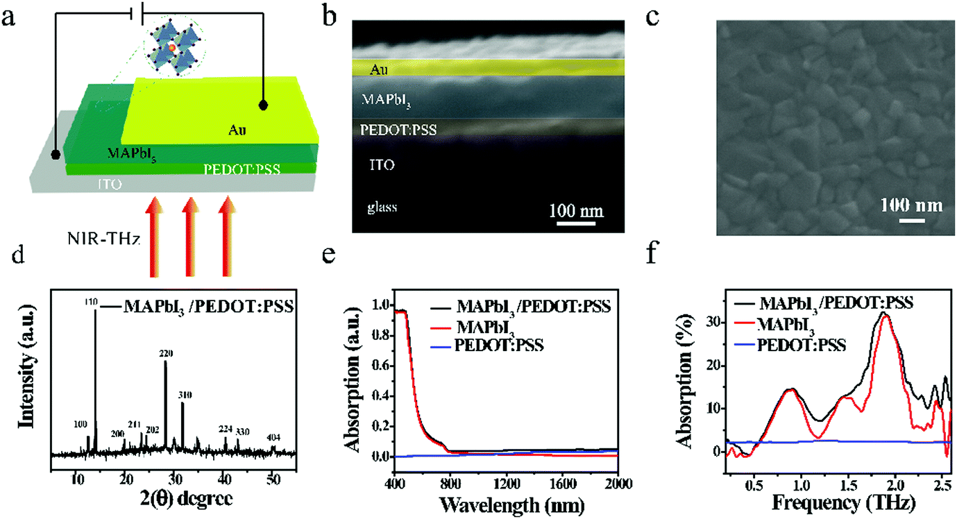 | ||
| Fig. 1 (a) Schematic illustration of the MAPbI3/PEDOT:PSS PD. (b) Cross-sectional image of the device with the structure of ITO/PEDOT:PSS/MAPbI3/Au. (c) Surface SEM image of the MAPbI3/PEDOT:PSS film. (d) XRD pattern of the MAPbI3/PEDOT:PSS film. (e) UV-NIR absorption spectra of MAPbI3, PEDOT:PSS and MAPbI3/PEDOT:PSS. (f) THz TDS spectra of MAPbI3, PEDOT:PSS and MAPbI3/PEDOT:PSS. | ||
The photoelectric characteristics of the MAPbI3/PEDOT:PSS PD were investigated under dark conditions and at different laser powers at 1064 nm and 2.52 THz. The I–V curves obtained from the MAPbI3/PEDOT:PSS PD under 1064 nm and 2.52 THz laser irradiation at different laser power densities are shown in Fig. 2a and b, respectively. It is obvious that in the small bias voltage range, the I–V curves exhibit an Ohmic characteristic and the curves shift upon light illumination, which are typical PTE effect features.13,33 The curves indicate that photocurrent increases with increasing laser power intensity in the −5 mV to 5 mV range of bias voltage. The I–V curves obtained over a wider bias voltage range from −1 V to 1 V are shown in Fig. S3 (ESI†). Under excitation of a large bias voltage, a Schottky barrier was formed in the device, because of different functions, which is consistent with the previously reported results.26 To quantify the junction current of the device under light illumination, logarithmic I–V characteristics of the device under 1064 nm and 2.52 THz illumination are shown in Fig. 2c and d, respectively. As shown in Fig. 2c and d, under dark conditions, a −0.31 V open circuit voltage Voc can be observed. And a net photocurrent is generated by the built in field even at zero bias. With the laser power increasing, the Voc shifts to a low negative voltage, which could be attributed to the generation of PTE voltage. Moreover, with increasing power intensity, the short-circuit current Isc changed, indicating an increase in the number of hot carriers under light illumination. The photocurrent generation mechanism is discussed fully here. Fig. 2e illustrates the band energy of the device and the charge transfer under dark conditions. Holes transfer towards the PEDOT:PSS layer while electrons tend to drift to the Au electrode, because of the different functions of the different layers. A built in field Ein forms in the device and its direction is from the Au electrode to the ITO electrode. This Ein direction of the device is opposite to the external circuit, as shown in Fig. 1a, and this results in the negative Voc being obtained under dark conditions. Under light illumination on the ITO electrode, a photo induced temperature gradient is produced, as shown in Fig. 2f. Upon thermal excitation, the hot carriers are transported from the PEDOT:PSS layer to the MAPbI3 layer, forming a Seebeck field, which is also called a PTE field EPTE. The direction of EPTE points from the ITO electrode towards the Au electrode. This PTE field is opposite in orientation to the built-in field, which leads to the positive shift of Voc. In this device, the photocurrent generation is mainly determined by the hot carrier transport. According to the Seebeck effect, the PTE voltage can be defined as ΔV = ΔS × ΔT, where ΔS is the Seebeck difference between the different layers and ΔT is the temperature gradient of the device under light irradiation.
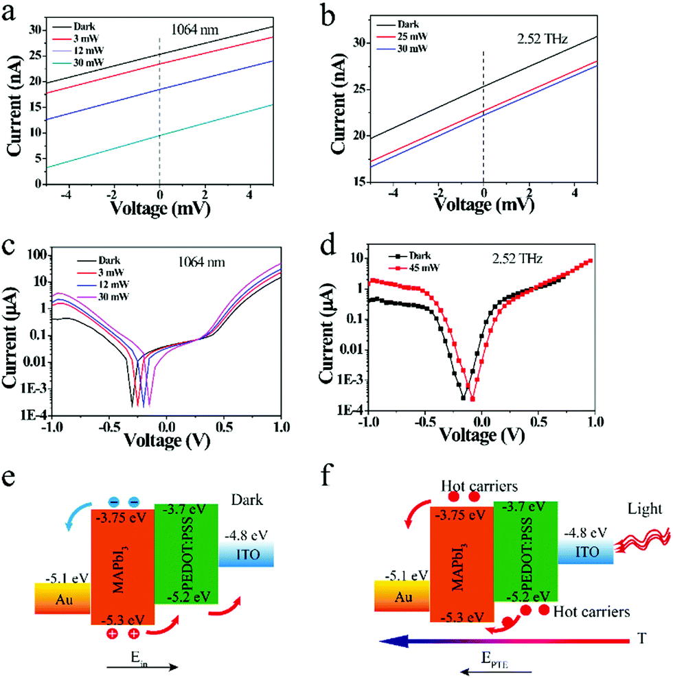 | ||
| Fig. 2 Current–voltage (I–V) characteristics of the MAPbI3/PEDOT:PSS device in the dark and under light illumination with different power intensities at (a) 1064 nm and (b) 2.52 THz. The logarithmic I–V characteristics of the device in the dark and under light illumination with different power intensities at (c) 1064 nm and (d) 2.52 THz. Schematic of the energy band and charge transfer at the MAPbI3/PEDOT:PSS interface (e) in the dark and (f) under light illumination. | ||
Additionally, the photoresponses of the MAPbI3/PEDOT:PSS PD were investigated under irradiation at 1064 nm and 2.52 THz. Fig. 3a shows the time-dependent photocurrent responses of the device produced by periodically turning the light illumination on and off under 1064 nm laser illumination at 0 V bias voltage. It is obvious that the device photocurrent increased with increasing power, thus demonstrating good on/off switching behaviors. The photocurrent increases from 0.8 nA to 6 nA when the incident light intensity varies from 0.8 mW to 11.5 mW. Moreover, the time-dependent photocurrents exhibit stable and repeatable characteristics, thus indicating the excellent stability of the device under 1064 nm laser irradiation. According to the obtained photocurrents under different laser power, the device responsivity (R) was calculated by the formula (1):
 | (1) |
 | (2) |
| NEP = √A/D* | (3) |
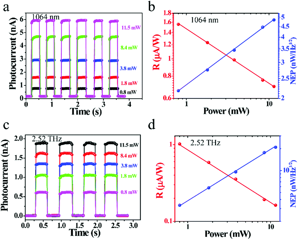 | ||
| Fig. 3 (a) Time-dependent photocurrents of the device under switching on/off 1064 nm illumination. (b) R and NEP of the device as a function of 1064 nm laser power intensity. (c) Time-dependent photocurrents of the devices under switching on/off 2.52 THz illumination. (d) R and NEP of the device as a function of 2.52 THz laser power intensity. | ||
Fig. 3c shows the optical switched on/off photocurrents of the device under 2.52 THz irradiation with varying power intensities at 0 V bias voltage. The photocurrents present stable and repeatable characteristics under different power intensities and increase from 0.6 to 1.8 nA with increasing laser power from 0.8 to 11.5 mW. Similarly, the photocurrents illustrate the good stability of the device under 2.52 THz laser irradiation. R and NEP are both plotted as a functions of power intensity in Fig. 3d. It shows that the R curve displays a decreasing trend while the NEP curve shows an increasing tendency with increasing power intensity, revealing the highest R value of 1.0 μA W−1 and the lowest NEP value of 3.3 nW Hz−1/2. R and P present a linear relationship when plotted in the double-logarithmic coordinates and can be expressed as log R ∼ αlogP, where α is a parameter without units. According to the reported results, the PTE photocurrent has a nonlinear dependence of 1/Tβ−1,10 while T has a power law dependence on Pγ.3 Then, R can be expressed as log R ∼ αlogP. The D curves with units of cm Hz1/2 W−1 under irradiation at 1064 nm and 2.52 THz are plotted as a function of power intensity in Fig. S4 (ESI†).
Based on the photoresponses obtained under NIR and THz illumination, the photocurrent generation mechanism can now be discussed fully. Many physical mechanisms may be responsible for the photoresponse of the MAPbI3/PEDOT:PSS PD, including the PC effect, PV effect, bolometric effect, pyroelectric effect and PTE effect. PC and PV effects are limited to the detection wavelength range wherein the photon energies are larger than the band gap of the effective material.11 The photon energy of NIR and THz is smaller than the 1.5 eV energy band gap of the device, as shown in Fig. 2e. Therefore, PC and PV effects cannot be used to explain the photocurrent generation. In contrast, thermoelectric effects are related to photoinduced hot carriers, which are independent of the incident wavelength. It is well known that the bolometric effect must work under the application of a bias voltage.8 Since the MAPbI3/PEDOT:PSS PD operates at zero bias, the bolometric effect thus does not apply to the device. According to the time-dependent photocurrent characteristics of the device obtained when switching the 1064 nm and 2.52 THz illumination on and off, which are shown in Fig. 3a and c, respectively, the pyroelectric effect can be excluded.34 Therefore, the PC, PV, bolometric and pyroelectric effects are eliminated, meaning that the PTE effect is responsible for the photoresponse of the device.
To aid in further understanding the PTE effect in our proposed device, temperature distribution and changes of the device under 1064 nm and 2.52 THz light illumination were measured using a FLIR infrared imaging device. As shown in Fig. 4a and b, under dark conditions, the MAPbI3/PEDOT:PSS PD shows a relatively low temperature of about 22.6 °C. Under 1064 nm laser illumination at a power of 1 mW, the surface temperature (24.7 °C) increased by 2.1 °C. The photocurrent and temperature gradient ΔT of the device measured under 1064 nm optical switching on/off at 0 V bias voltage are shown in Fig. 4c. The results show that over multiple optical switching cycles, the trend of photocurrent changes is consistent with that of temperature change. Similarly, the infrared images in Fig. 4d and e clearly show the surface temperature distribution of the device under 2.52 THz irradiation. The device shows a relatively low temperature of approximately 22.6 °C in the dark. Under 2.52 THz laser illumination at a power of 0.3 mW, the surface temperature (23 °C) increased by 0.4 °C. Furthermore, photocurrent at 0 V and temperature switching curves with the same tendency were acquired and are presented in Fig. 4f. As illustrated in Fig. 2f, upon light irradiation, a temperature gradient forms throughout the device; meanwhile, photocurrent generation depends on the hot carrier transport. The Seebeck coefficient values of MAPbI3, PEDOT:PSS and MAPbI3/PEDOT:PSS films are plotted as a function of temperature in Fig. S5 (ESI†). By constructing a heterojunction structure, the Seebeck coefficient of the device increases greatly. The highest value of ∼532 μV K−1 at 45 °C is one order of magnitude higher than that of the pure MAPbI3 device.26 As shown in Fig. 4c and f, the device displays 2 K and 0.4 K temperature differences under 1064 nm (1 mW) and 2.52 THz (0.3 mW) illumination, respectively. According to the PTE effect, the photovoltage can be defined as ΔV = ΔS × ΔT (ΔV1064 nm = 1.05 mV and ΔV2.52 THz = 0.199 mV) under 1064 nm and 2.52 THz illumination. The photocurrent can be expressed as I = ΔV/Rh, where Rh is the device resistance and the value of Rh is approximately 1 × 10⁶ Ω, as shown in Fig. 2a and b. Then, the photocurrents of the device can be calculated to be 1 nA and 0.2 nA under 1064 nm (1 mW) and 2.52 THz (0.3 mW) illumination, respectively, and these values are consistent with the experimental values given in Fig. 4c and f. Therefore, both the experimental results and the theoretical analysis confirm that the PTE effect dominates the photocurrent generation in the MAPbI3/PEDOT:PSS PD.
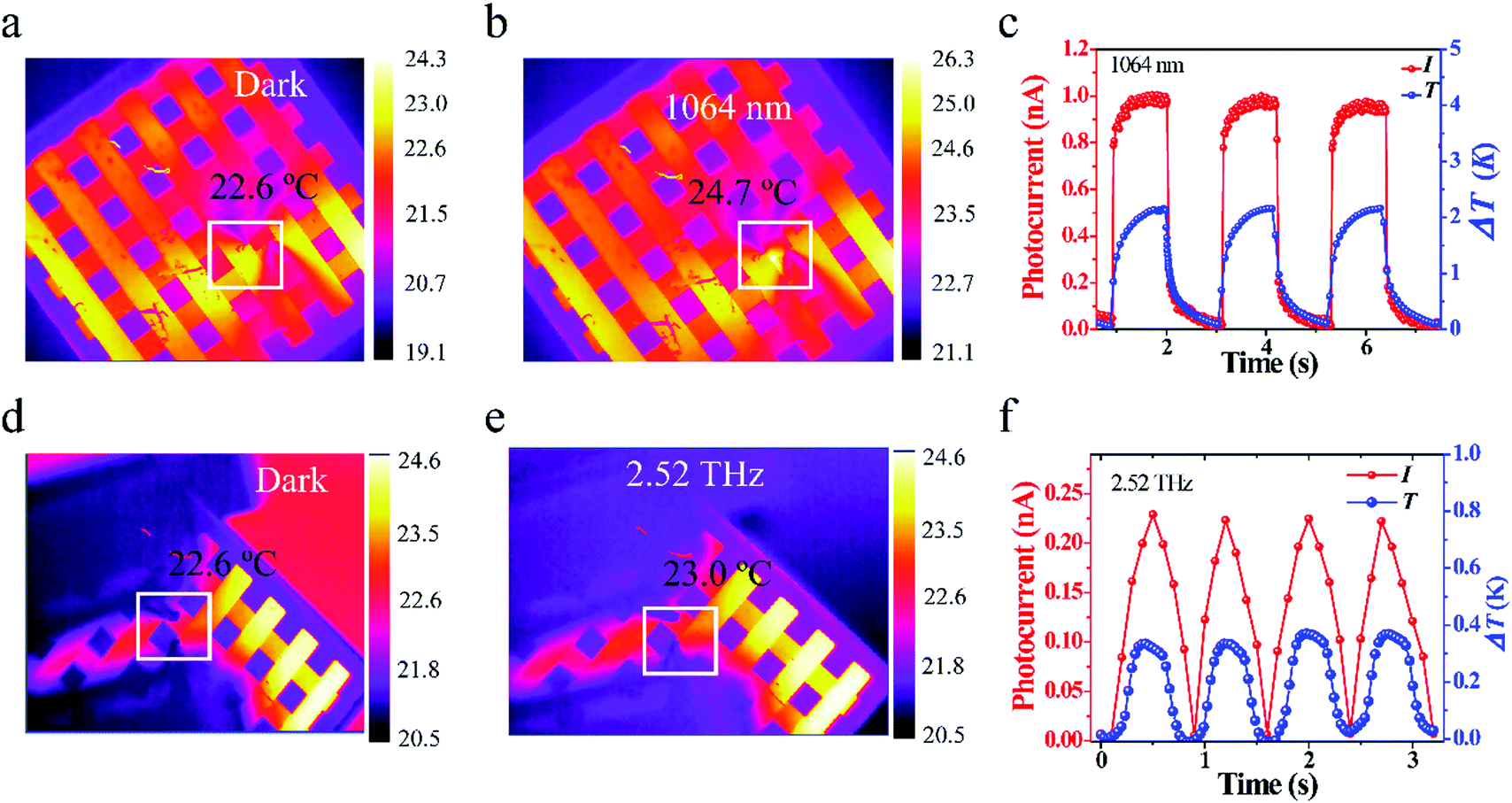 | ||
| Fig. 4 Thermoelectric response mechanism of the device. (a and b) Temperature (T) distributions of the device in the dark and under 1064 nm laser illumination (0.8 mW), respectively. (c) Photocurrent and ΔT of the device under switching on/off 1064 nm at 0.8 mW. (d and e) Temperature (T) distributions of the device in the dark and under 2.52 THz laser illumination (0.8 mW), respectively. (f) Photocurrent and ΔT of the device under switching on/off 2.52 THz at 0.8 mW. | ||
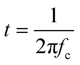
Response speed is another important performance parameter for a PD. Fig. 5a shows a schematic diagram of the response time test system used for the device. The 1064 nm laser was modulated by a wave generator to produce specific frequency switching laser. A resistor with equivalent resistance to that of the MAPbI3/PEDOT:PSS PD is used in the series circuit. Then, the response time can be recorded by using an oscilloscope. Fig. 5b displays the normalized responsivity with respect to the modulation frequency under 1064 nm irradiation at 0 V bias voltage. The −3 dB bandwidth of the device was acquired at 5 kHz. The relationship between the response time and the −3 dB bandwidth frequency is shown below:
 | (4) |
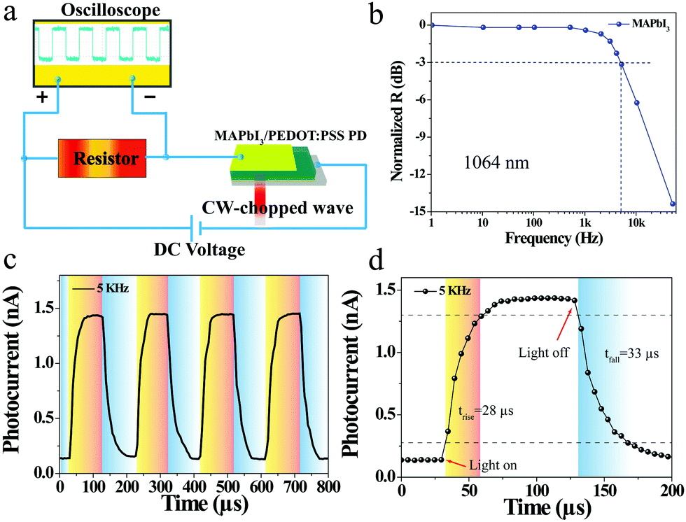 | ||
| Fig. 5 (a) Schematic diagram of time response test system of the device. (b) Normalized responsivity as a function of modulation frequency under 1064 nm irradiation and the f−3 dB bandwidth of the device. Photocurrent response of the device under 1064 nm laser irradiation with the frequency of 5 kHz: (c) multiple cycles and (d) one cycle with the rise and fall time. | ||
The Seebeck coefficients of MAPbI3, PEDOT:PSS and MAPbI3/PEDOT:PSS under different light irradiation with 0.8 mW power are shown in Table S1 (ESI†). The carrier concentration (n), Hall mobility (μH), and calculated conductivity (σH) of the MAPbI3/PEDOT:PSS PD obtained by using a Hall test system are shown in Table S2 (ESI†). Moreover, a comparison of the critical parameters of PEDOT:PSS based composite photodetectors is presented in Table 1.27,37–40 And the comparison of the critical parameters of PTE photodetectors based on thermoelectric materials is presented in Table 2.3,12,13,27,41 When compared with the reported results, the MAPbI3/PEDOT:PSS PD displays the fastest response speed and a relatively high detectivity. Moreover, the detection band of the MAPbI3/PEDOT:PSS device is extended to the THz range, which is advantageous for THz detection.
| Description | Wavelength | Responsivity (mA W−1) | Detectivity (Jones) | Response time | Ref. |
|---|---|---|---|---|---|
| PEDOT:PSS/graphene | 7.8 μm IR | 2.3 V W−1 (0 V bias) | 1.4 × 10⁷ | 20 s | 27 |
| Al: MgZnO/PEDOT:PSS | 278 nm UV-B | 19.1 mA W−1 (0 V bias) | — | 3.5 s | 37 |
| Single ZnO/PEDOT:PSS | 325 nm UV | 6.8 × 10⁻³ (0 V bias) | 9.3 × 10⁹ | 4.5 s | 38 |
| MAPbI3−xClx/PEDOT:PSS | 598–895 nm UV-NIR | 1.91 × 10⁹ (0.5 V bias) | 1.4 × 10¹⁴ | >50 s | 39 |
| PEDOT:PSS/ZnO | 300–400 nm UV | 2.5 × 10⁵ (−1 V bias) | 2.5 × 10¹¹ | 0.94 s | 40 |
| MAPbI3/PEDOT:PSS | 1064 nm–118 μm NIR-THz | 1.6 × 10⁻³ (0 V bias) | 1.2 × 10⁷ | 28 μs | This work |
| Description | Wavelength | Responsivity (mA W−1) | Detectivity (Jones) | Response time | Ref. |
|---|---|---|---|---|---|
| 3D graphene foams | 405 nm–118 μm UV-THz | 0.2–0.05 (0.05 bias) | 7.7 × 10⁶ | 48 ms | 3 |
| RGO films | 375 nm–118 μm UV-THz | 87.3–2.8 mV W−1 (0 V bias) | 4.23 × 10⁶ | 34 ms | 12 |
| EuBiSe3 crystal | 405 nm–118 μm UV-THz | 1.25–0.69 V W−1 (0 V bias) | 2.91 × 10⁸ | 207 ms | 13 |
| PEDOT:PSS/graphene | 7.8 μm IR | 2.3 V W−1 (0 V bias) | 1.4 × 10⁷ | 20 s | 27 |
| 3D MG | 118 μm THz | 5.1 mV W−1 (0 V bias) | 2.5 × 10⁵ | 23 ms | 41 |
| MAPbI3/PEDOT:PSS | 1.064–118 μm NIR-THz | 1.6 × 10⁻³ (0 V bias) | 1.2 × 10⁷ | 28 μs | This work |
3. Conclusions
In summary, we proposed a fast response self-powered NIR and THz PTE PD that was assembled using a structure of ITO/PEDOT:PSS/MAPbI3/Au. By constructing the PEDOT:PSS/MAPbI3 junction, the enhanced Seebeck coefficient and high electrical conductivity were investigated. Subsequently, the photoresponse and response speed of the device were optimized under 1064 nm and 2.52 THz irradiation. Furthermore, the PTE PD shows a high response speed of 28 μs with a −3 dB bandwidth of 5 kHz. These results indicate that the PEDOT:PSS/MAPbI3 composition is a good candidate material for fabricating high speed, self-powered and room temperature operation NIR and THz optoelectronic devices.4. Experimental details
Synthesis of MAPbI3
The MAPbI3 thin film was grown by using an antisolvent method. The MAPbI3 perovskite precursor solution was prepared by dissolving a mixture of PbI2 (99.99%) and MAI (99%) by using a molar ratio of 1:1. The mixture dissolved in a mixed solvent DMF (99.5%) and DMSO (99.5%) with a volume ratio of 7:3. The precursor solution was spin-coated on the substrate with a rotate speed of 6000 rpm. After a delay time of 40 s, 150 μL of the antisolvent CB was dripped onto the films. Then, the film was annealed in a glove box at 100 °C for 40 s.
Fabrication process of the Au/MAPbI3/PEDOT:PSS/ITO PD
The Au/MAPbI3/PEDOT:PSS/ITO PDs were fabricated as follows. A quartz glass sheet coated with an indium tin oxide (ITO) film served as the substrate. The ITO/glass substrate with dimensions of 14 × 14 × 2 mm was handled within a UV-ozone system for 15 min. Then, a PEDOT:PSS aqueous solution (bought from Xi'an Polymer Light Technology Corp) was deposited onto the substrate via spin coating at a rotation speed of 5000 rpm, 50 s. Subsequently, the PEDOT:PSS film was heated at 150 °C for 30 min and was then transferred into a glove box. The MAPbI3 perovskite film was then spin-coated onto the ITO/PEDOT:PSS film substrate. After the coating process was complete, the samples were placed in a vacuum chamber with a vacuum of 10−4 Pa. The electrodes were then prepared by the thermal evaporation method on the MAPbI3 perovskite film from Cr/Au (10/200 nm) layers using a shadow mask.Characterization and testing
The device's cross and surface morphologies were examined by using scanning electron microscopy (SEM) and Atomic Force Microscopy (AFM). The structure of the device was obtained by X-Ray Powder Diffraction (XRD). The photoluminescence (PL) spectrum was recorded using 374 nm laser. The I–V characteristics and the photocurrents of the device were tested by using a Keithley 2400 source meter with Labview software. The light sources were 1064 nm semiconductor lasers and a 118 μm terahertz source (FIRL 100). The light power was measured by using a power meter with an RS232 port (Ophir Vega). The broadband absorption spectra of the device were recorded using a Zolix Omni-λ 3007 spectrophotometer with Si and InGaSn photodetectors. The absorption performance of MAPbI3 in the THz range was tested using a terahertz time-domain spectroscopy system. The temperature images of the device were obtained by using an Infrared thermal imager (FLIR T630sc). The Seebeck coefficient was measured by using a self-built test system. A heating band was used to produce a temperature difference of the channel. The voltage difference (ΔV) between the two electrodes was measured by using a Keithley 2400 source meter and the temperature distribution was obtained by using the Infrared thermal imager. The Seebeck coefficient was calculated as S = ΔV/ΔT, where ΔT = Thot − Tcold, meaning the temperature difference between the hot side and cold side.Conflicts of interest
There are no conflicts to declare.Acknowledgements
This work was supported by the National Natural Science Foundation of China (No. 61675147, 61735010 and 91838301), the National Key Research and Development Program of China (No. 2017YFA0700202), Basic Research Program of Shenzhen (JCYJ20170412154447469), and Beiyang yong junior faculties of Tianjin university (No. 2019XRG-0056).References
- Y. Cao, J. Zhu, J. Xu, J. He, J. L. Sun, Y. Wang and Z. Zhao, Small, 2014, 10, 2345–2351 CrossRef CAS PubMed.
- Y. Liu, J. Yin, P. Wang, Q. Hu, Y. Wang, Y. Xie, Z. Zhao, Z. Dong, J.-L. Zhu, W. Chu, N. Yang, J. Wei, W. Ma and J.-L. Sun, ACS Appl. Mater. Interfaces, 2018, 10, 36304–36311 CrossRef CAS PubMed.
- Y. Z. Yifan Li, Y. Yu, Z. Chen, Q. Li, T. Li, J. Li, H. Zhao, Q. Sheng, F. Yan, Z. Ge, Y. Ren, Y. Chen and J. Yao, Photonics Res., 2020, 8, 368–374 CrossRef.
- H. C. Zhiyu Huang, Y. Huang, Z. Ge, Y. Zhou, Y. Yang, P. Xiao, J. Liang, T. Zhang, Q. Shi, G. Li and Y. Chen, Adv. Funct. Mater., 2017, 28, 8 Search PubMed.
- C. Liu, L. Wang, X. Chen, J. Zhou, W. Hu, X. Wang, J. Li, Z. Huang, W. Zhou, W. Tang, G. Xu, S.-W. Wang and W. Lu, Carbon, 2018, 130, 233–240 CrossRef CAS.
- M. S. Vitiello, D. Coquillat, L. Viti, D. Ercolani, F. Teppe, A. Pitanti, F. Beltram, L. Sorba, W. Knap and A. Tredicucci, Nano Lett., 2012, 12, 96–101 CrossRef CAS PubMed.
- Y. Chen, X. Wang, G. Wu, Z. Wang, H. Fang, T. Lin, S. Sun, H. Shen, W. Hu, J. Wang, J. Sun, X. Meng and J. Chu, Small, 2018, 14, 1703293 CrossRef PubMed.
- Q. Han, T. Gao, R. Zhang, Y. Chen, J. Chen, G. Liu, Y. Zhang, Z. Liu, X. Wu and D. Yu, Sci. Rep., 2013, 3, 3533 CrossRef PubMed.
- C. C. E. Peytavit and J.-F. Lampin, J. Appl. Phys., 2011, 109, 016101 CrossRef.
- X. Xu, N. M. Gabor, J. S. Alden, A. M. Van Der Zande and P. L. Mceuen, Nano Lett., 2010, 10, 562–566 CrossRef CAS PubMed.
- F. H. Koppens, T. Mueller, P. Avouris, A. C. Ferrari, M. S. Vitiello and M. Polini, Nat. Nanotechnol., 2014, 9, 780–793 CrossRef CAS PubMed.
- Y. N. Jianguo Wen, P. Wang, M. Chen, W. Wu, Y. Cao, J.-L. Sun, M. Zhao, D. Zhuang and Y. Wang, Carbon, 2019, 153, 274–284 CrossRef.
- Y. N. Yingxin Wang, M. Chen, J. Wen, W. Wu, Y. Jin, D. Wu and Z. Zhao, ACS Photonics, 2019, 6, 895–903 CrossRef.
- M. Buscema, M. Barkelid, V. Zwiller, H. S. Van Der Zant, G. A. Steele and A. Castellanos-Gomez, Nano Lett., 2013, 13, 358–363 CrossRef CAS PubMed.
- S. Limpert, A. Burke, I. J. A. Chen, N. S. Lehmann, S. Fahlvik, S. Bremner, G. Conibeer, C. Thelander, M. E. Pistol and H. Linke, Nano Lett., 2017, 17, 4055–4060 CrossRef CAS PubMed.
- A. V. Emelianov, D. Kireev, A. Offenhäusser, N. Otero, P. M. Romero and I. I. Bobrinetskiy, ACS Photonics, 2018, 5, 3107–3115 CrossRef.
- X. Cai, A. B. Sushkov, R. J. Suess, M. M. Jadidi, G. S. Jenkins, L. O. Nyakiti, R. L. Myers-Ward, S. Li, J. Yan, D. K. Gaskill, T. E. Murphy, H. D. Drew and M. S. Fuhrer, Nat. Nanotechnol., 2014, 9, 814–819 CrossRef CAS PubMed.
- Y. F. Li, Y. T. Zhang, Z. Chen, Q. Li, T. Li, M. Li, H. Zhao, Q. Sheng, W. Shi and J. Q. Yao, Photon. Res., 2020, 8, 1301–1308 CrossRef.
- N. Alwadai, M. A. Haque, S. Mitra, T. Flemban, Y. Pak, T. Wu and I. Roqan, ACS Appl. Mater. Interfaces, 2017, 9, 37832–37838 CrossRef CAS PubMed.
- F. Huang, Y. Peng and G. Liu, J. Phys. Chem. C, 2019, 123, 11073–11080 CrossRef CAS.
- S. Tong, J. Sun, C. Wang, Y. Huang, C. Zhang, J. Shen, H. Xie, D. Niu, S. Xiao, Y. Yuan, J. He, J. Yang and Y. Gao, Adv. Electron. Mater., 2017, 3, 1700058 CrossRef.
- M. Kim, G.-H. Kim, T. K. Lee, I. W. Choi, H. W. Choi, Y. Jo, Y. J. Yoon, J. W. Kim, J. Lee, D. Huh, H. Lee, S. K. Kwak, J. Y. Kim and D. S. Kim, Joule, 2019, 3, 2179–2192 CrossRef CAS.
- S. S. Shin, S. J. Lee and S. I. Seok, Adv. Funct. Mater., 2019, 29, 1900455 CrossRef CAS.
- Y. Li, Y. Zhang, T. Li, M. Li, Z. Chen, Q. Li, H. Zhao, Q. Sheng, W. Shi and J. Yao, Nano Lett., 2020 DOI:10.1021/acs.nanolett.0c00082.
- A. Pisoni, J. Jacimovic, O. S. Barisic, M. Spina, R. Gaal, L. Forro and E. Horvath, J. Phys. Chem. Lett., 2014, 5, 2488–2492 CrossRef CAS PubMed.
- Y. Xiong, L. Xu, P. Wu, L. Sun, G. Xie and B. Hu, Adv. Funct. Mater., 2019, 29, 1900615 CrossRef.
- J. T. W. Y. Mingyu Zhang, Carbon, 2020, 156, 339–345 CrossRef.
- K. C. Choongho Yu, L. Yin and J. C. Grunlan, ACS Nano, 2011, 5, 7885–7892 CrossRef PubMed.
- N. Massonnet, A. Carella, O. Jaudouin, P. Rannou, G. Laval, C. Celle and J.-P. Simonato, J. Mater. Chem. C, 2014, 2, 1278–1283 RSC.
- T.-C. Tsai, H.-C. Chang, C.-H. Chen and W.-T. Whang, Org. Electron., 2011, 12, 2159–2164 CrossRef CAS.
- C. Xieand and F. Yan, ACS Appl. Mater. Interfaces, 2017, 9, 1569–1576 CrossRef PubMed.
- C. Xieand and F. Yan, J. Mater. Chem. C, 2018, 6, 1338–1342 RSC.
- Y. S. Lai, C. Y. Tsai, C. K. Chang, C. Y. Huang, V. K. Hsiao and Y. O. Su, Adv. Mater., 2016, 28, 2644–2648 CrossRef CAS PubMed.
- L. Jin, Y. Zhang, Y. Yu, Z. Chen, Y. Li, M. Cao, Y. Che and J. Yao, Adv. Opt. Mater., 2018, 6, 1800639 CrossRef.
- F.-X. Liang, J.-Z. Wang, Z.-X. Zhang, Y.-Y. Wang, Y. Gao and L.-B. Luo, Adv. Opt. Mater., 2017, 5, 1700654 CrossRef.
- H. Zhao, Y. Zhang, T. Li, Q. Li, Y. Yu, Z. Chen, Y. Li and J. Yao, Nanotechnology, 2020, 31, 035202 CrossRef PubMed.
- Q. Zheng, J. Huang, C. Han and Y. Chen, IEEE Electron Device Lett., 2017, 38, 79–82 CAS.
- F. Yi, Q. Liao, Y. Huang, Y. Gu and Y. Zhang, Semicond. Sci. Technol., 2013, 28, 105023 CrossRef.
- C. Xie, P. You, Z. Liu, L. Li and F. Yan, Light: Sci. Appl., 2017, 6, e17023 CrossRef PubMed.
- S. Dhar, T. Majumder, P. Chakraborty and S. P. Mondal, Org. Electron., 2018, 53, 101–110 CrossRef CAS.
- Y. W. Meng Chen, J. Wen, H. Chen, W. Ma, F. Fan, Y. Huang and Z. Zhao, ACS Appl. Mater. Interfaces, 2019, 11, 6411–6420 CrossRef PubMed.
Footnote |
| † Electronic supplementary information (ESI) available: The AFM surface morphology of the MAPbI3 film, the PL spectra of the MAPbI3/PEDOT:PSS thin film, the I–V curves in a wider range of −1 V to 1 V bias voltage, the D curve under 1064 nm and 2.52 THz irradiation as a function of power intensity, and the Seebeck coefficient of the MAPbI3/PEDOT:PSS device. See DOI: 10.1039/d0tc02399j |
| This journal is © The Royal Society of Chemistry 2020 |