
 Open Access Article
 This Open Access Article is licensed under a
 Creative Commons Attribution 3.0 Unported Licence
Near infrared organic photodetectors based on enhanced charge transfer state absorption by photonic architectures†
Martí
Gibert-Roca
 ,
Pau
Molet
,
Agustín
Mihi
* and
Mariano
Campoy-Quiles
*
,
Pau
Molet
,
Agustín
Mihi
* and
Mariano
Campoy-Quiles
*
Institut de Ciència de Materials de Barcelona (ICMAB-CSIC), E-08193 Cerdanyola del Vallès, Spain. E-mail: amihi@icmab.es; mcampoy@icmab.es; m.campoy@csic.es
First published on 15th June 2020
Abstract
Near infrared photodetectors are a widespread and fundamental technology in many disciplines, from astronomy and telecommunications to medical sciences. Current technologies are now striving to include new aspects in this technology such as wearability, flexibility and tunability. Organic photodetectors easily offer many of those advantages but their relatively high bandgaps hinder NIR operation. In this work, we demonstrate solution processed organic photodetectors with improved NIR response thanks to a nanostructured active layer in the shape of a photonic crystal. The latter strongly increases the charge transfer state absorption, which is normally weak but broadband, increasing the optical path of light and resulting in remarkable photoresponse significantly below the band gap of the blend. We show responsivities up to 50 mA W−1 at 900 nm for PBTTT:PC71BM based photodetectors. On top of that, by varying the lattice parameter of the photonic crystal structure, the spectral response of the photodetectors can be tuned beyond 1000 nm. Furthermore, our photonic structure can be easily implemented in the device in a single nanoimprinting step, with minimal disruption on the fabrication process, which makes this approach very promising for upscaling.
1. Introduction
Nowadays, near infrared (NIR) photodetectors are a ubiquitous technology, used on a daily basis in applications such as automatic sliding doors, NIR cameras, remote controls, telecommunications, spectrophotometers, and medical diagnosis.1,2 Current NIR photodetector technologies rely on combining silicon or, to a lesser extent, III–V (InGaAs) with color filters or gratings.3,4 This approach has proven to be functional and reliable, however, such wafer based photodetectors with extra filtering components fail to satisfy the new demands for wearable, cheap and flexible devices. In this direction, organic photodetectors (OPDs) are emerging as an appealing alternative, thanks to their flexibility, low embedded energy processing and high compatibility with available and easily scalable techniques such as roll to roll processing.5–8 Ease and cost of manufacture is not the sole advantage, since the composing organic polymers and/or small organic molecules, can be chemically tuned to provide a variety of absorption ranges.9–11 While this approach has worked well in the visible range, extending the photoresponse towards the NIR range has been challenging. Lower bandgap polymers and small molecules with responses that go deeper into the infrared are being synthesized,12,13 however, these new materials are complex and expensive, both in time and energy, reducing their potential to be used in real devices.12 Moreover, new molecules have to be developed for each targeted wavelength range, strongly increasing the required synthetic efforts.Alternatively, some effort has been devoted to extend and increase the absorption in the NIR region with inexpensive and readily available materials using new inventive designs.14,15 One approach that rendered promising results is the filtering effect in thick polymer layers, also known as charge collection narrowing,16 to obtain narrow and high external quantum efficiencies (EQE) in the NIR. However, since this approach relies on the intrinsic absorption of the materials, it still requires relatively low bandgap materials to reach into the NIR region.
A recently proposed elegant alternative is to take advantage of the direct intermolecular charge transfer state (CTS) absorption, extending the photoresponse into the NIR region without the need of low bandgap materials.17–20 The CTS is the result of the interaction between the highest occupied molecular orbital (HOMO) of the donor and the lowest unoccupied molecular orbital (LUMO) of the acceptor. This state appears only at the donor–acceptor interface, where the different electronic orbitals come together forming a new, intermediate state. The latter usually has a significantly lower transition energy than the corresponding constituents in a type II heterojunction, such as typical donor/acceptor blends. In other words, the HOMO energy level of the donor is higher than that of the acceptor and the LUMO energy level of the acceptor is lower than that of the donor (staggered gap). Since the CTS has a lower transition energy, the blend can potentially absorb light with photon energies below the bandgaps of each of its separate components. The CTS absorption strength depends on the intermixing of the molecules and, unfortunately, is around two orders of magnitude lower than singlet absorption due to the fact that it is an intermolecular state.13 The intrinsic low oscillator strength of the CTS often requires the use of very thick active layers at high reverse voltages in order to obtain a significant photoresponse.21 In a traditional device configuration, in order to enhance the absorption of the CTS, the thickness of the active layer must be increased enormously (tenths of microns); this implies the usage of hundreds of Volts applied bias to extract charges efficiently.21 In order to avoid such high voltages and thick layers, light trapping schemes offer an interesting alternative to greatly enhance the CTS absorption. Recently, the use of metal cavities has led to an impressive photoresponse in OPDs beyond the bandgaps of the composing materials.22–25 When using optical micro-cavities the detection wavelength can be tuned by accurately controlling the cavity dimensions, i.e., the active layer thickness. While these devices exhibit a very good performance, the resonant frequency critically depends on film thickness, thus they may not be compatible with techniques such as roll to roll, in which thickness usually fluctuates within a certain tolerance.
Inspired by the micro-cavity devices, in this work we propose a device configuration that will enhance the CTS absorption effect via a nanostructured active layer in the shape of a photonic crystal.26 Major accomplishments have been achieved already in photovoltaics by structuring the device with photonic crystals.27–30 In the case of 2D photonic crystals, its periodic structure diffracts incident light and enhances the optical path within the active layer, thus rendering higher efficiencies. In this work we will provide our photodetector with a back-electrode structured as a 2D photonic crystal engineered to couple incident light to photonic modes with enhanced electric field concentration in the active medium at those wavelengths of interest for the CTS absorption effect. To fulfill real application demands, the designed device has been fabricated with low cost blend materials using inexpensive and scalable techniques such as blade coating for the photodetector manufacturing and nanoimprinting soft-lithography for the active layer nanostructuration. The active layer blends are composed of a bulk heterojunction (BHJ) of an electron donor PBTTT or P3HT and an electron acceptor PC71BM or PC61BM. We show that these active layers can be easily and seamlessly nanostructured via soft nanoimprinting lithography, enhancing the EQE response from 750 to 1000 nm and from 775 to 1075 nm, for P3HT:PC61BM and PBTTT:PC71BM, respectively. We attribute this photoresponse, significantly beyond the band gap of the active layer, to the absorption of the CTS. Different photonic lattice parameters have been used to enhance the absorption at specific wavelengths, and thus to provide wavelength tuneability on the NIR region. Furthermore, since the enhanced photodetection wavelength is thickness independent, the processing tolerances can be higher, making this device attractive for further development and commercialization. In summary, the designed light trapping configuration implemented enables us to use inexpensive organic materials for photodetection into the NIR with minimal disruption of the fabrication process and where the nanostructuring step does not negatively affect the electrical performance of the photodetector.
2. Results and discussion
2.1 Device fabrication
The organic NIR photodetectors were fabricated from P3HT:PC61BM and PBTTT:PC71BM BHJ blends (chemical structure in Fig. 1a) for three main reasons: first, they are inexpensive materials, which makes them appealing for large scale applications; second, they exhibit a significant CTS absorption that extends into the NIR region, so we can extend the response of the devices beyond their band gaps; and third, they have sufficiently high carrier mobilities that allow us to deposit thick active layers, which is essential to take maximum profit of the CTS low absorption coefficient.13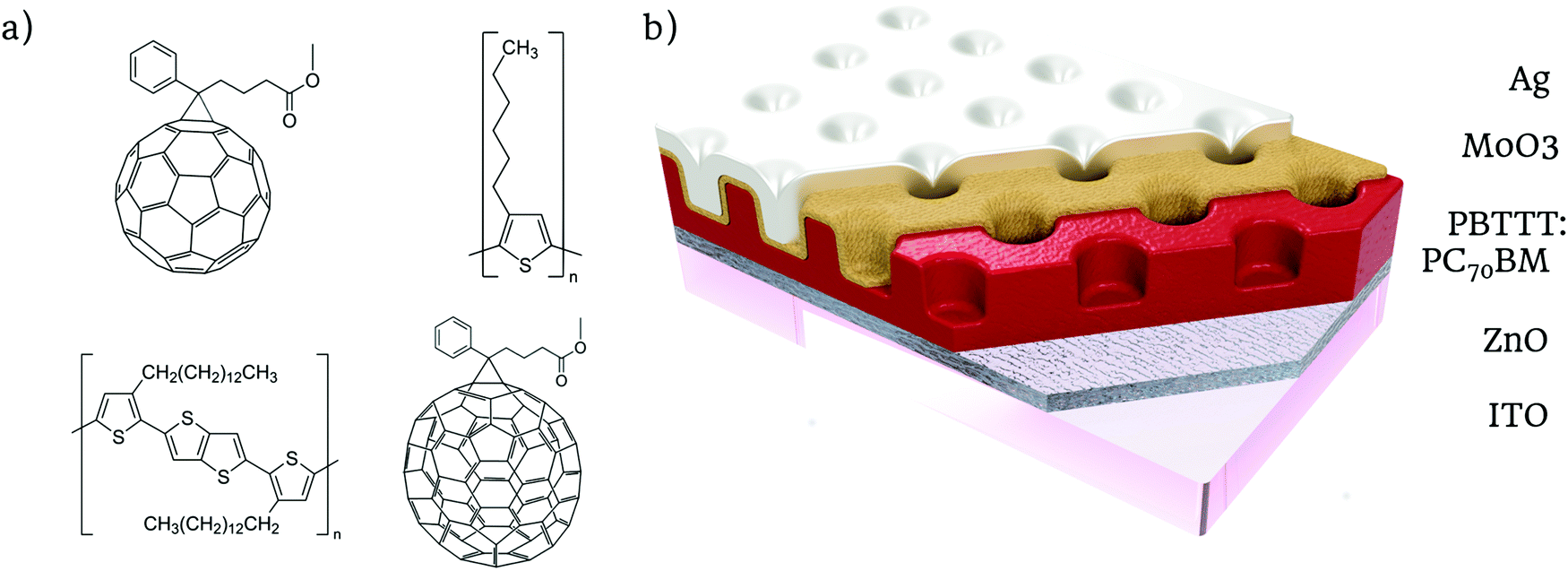 | ||
| Fig. 1 Schematics of the nanostructured organic NIR photodetector. (a) Phenyl-C61-butyric acid methyl ester (PC61BM) (>99.5%), poly(3-hexylthiophene-2,5-diyl) (P3HT), [6,6]-phenyl C71 butyric acid methyl ester (PC71BM) and poly[2,5-bis(3-tetradecylthiophen-2-yl)thieno[3,2-b]thiophene] (PBTTT-C14). (b) Diagram the organic photodetector structure and each layer's material. | ||
First, we deposited a ZnO electron transport layer (ETL) over the ITO covered glass substrates by blade coating a technique that is often used as a pre-upscaling method.
After annealing the film, we deposited a thick layer of active material also by blade coating. Then, we nanostructured the dry active layer via soft nanoimprinting lithography (Fig. 2a). This technique is reliable, cleanroom free, inexpensive and can produce extended nanostructured areas with high fidelity, plus it is highly scalable and compatible with roll to roll processes.31,32
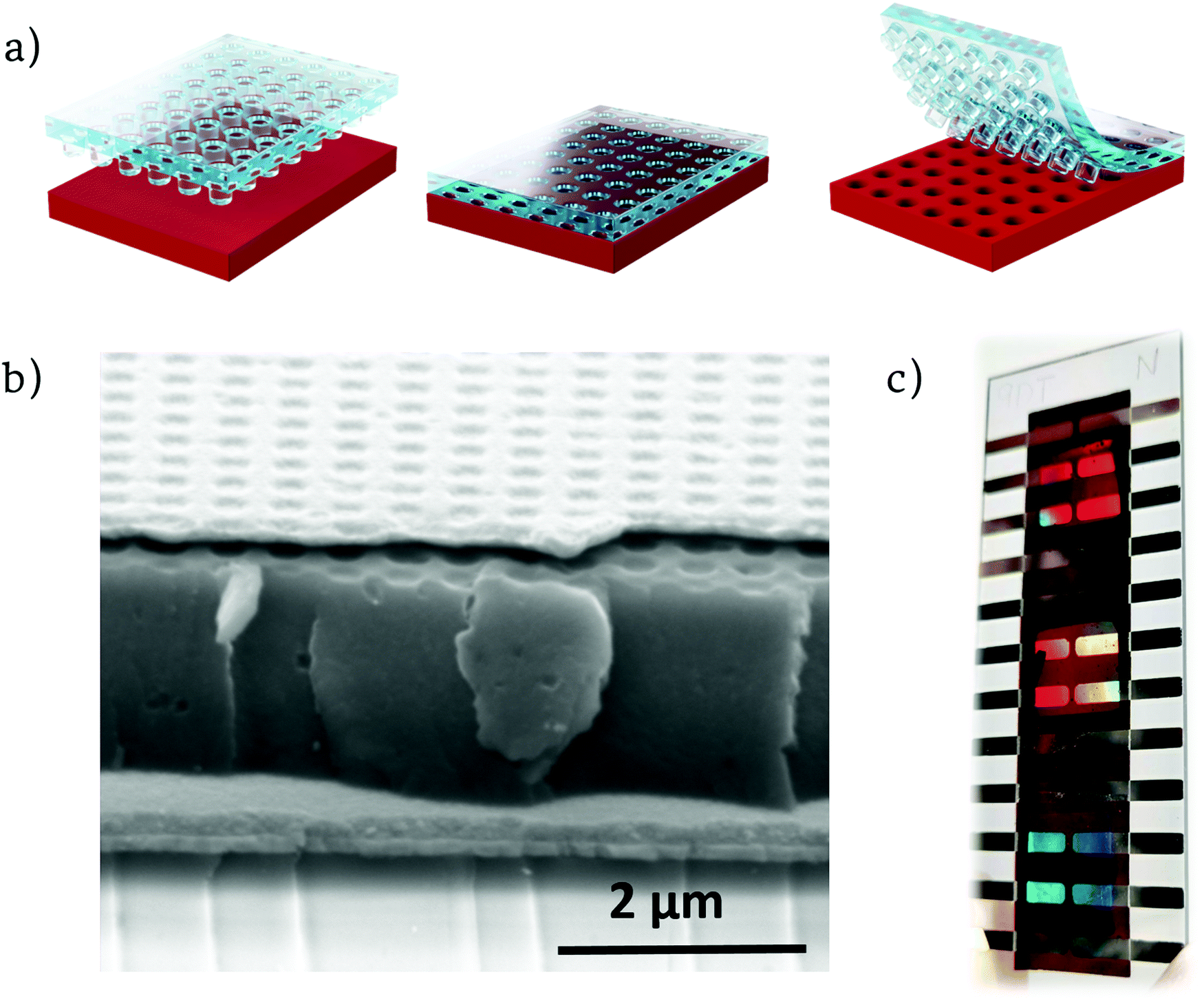 | ||
| Fig. 2 (a) Soft nanoimprinting lithography process steps. (b) SEM image of one of the finished nanostructured photodetectors. (c) Picture of the finished device showing different iridescence for each nanostructuration; L = 600, L = 500, L = 400 from top to bottom. | ||
Moreover, this non-disruptive technique avoids using aggressive nanostructuring processes, such as reactive ion etching, that could deteriorate the electrical properties of the device. Pressing a pre-patterned PDMS (polydimethyl siloxane) stamp mold onto the active layer at a temperature over the glass transition of the polymer blend is enough to produce the negative photonic crystal imprint on the device (see Experimental section). Our pattern consists of a square array of cylindrical pillars that acts as a diffraction grating, coupling the incident light into propagating modes of the active layer. We used Finite-Differences Time-Domain method (FDTD) to engineer the optimal photonic structures for our active materials and provide insight on the light propagation within the device (Fig. S1, ESI†). We concluded that, array lattice parameters (L) of 400, 500 and 600 nm (from now on also referred to as L = 400, L = 500 and L = 600) place their first orders of diffraction inside the range of absorption of the CTS. This would then provide efficient light trapping at NIR frequencies below the band gap of the BHJ materials, thus amplifying the CTS absorption. The thermally evaporated MoO3 layer thickness was set to 10 nm, enough to have a uniform film with good electrical performance while maintaining the optical properties of the device (Fig. S2, ESI†). Finally, a thick 200 nm Ag back electrode contact was evaporated onto the samples followed by a thermal annealing to increase their crystallinity (Fig. 2b and c). Since the back electrode was deposited onto the nanostructured active layer, it followed the corrugation resulting in a nanostructured back electrode (Fig. 2b) with a strong optical response (Fig. S3, ESI†).
2.2 Proof of concept photonic NIR device
The electrical characterization of our devices starts with EQE measurements. The EQE measurements of the devices with the photonic back electrode revealed several peaks in the NIR region that were absent in the reference flat samples (Fig. 3), for both active layer compositions.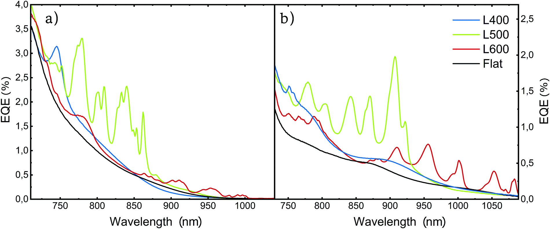 | ||
| Fig. 3 External quantum efficiency measurements for non-structured (flat) and differently nanostructured photodetectors (L = 400, L = 500 and L = 600) with an active layer of (a) P3HT:PC61BM, (b) PBTTT:PC71BM. | ||
As predicted by our simulations, the spectral range at which this enhanced EQE appears depends on the lattice parameter of the 2D array and the refractive index of the active layer. Both larger lattice parameters and higher active layer refractive indexes induce a redshift in the position of the peaks (Fig. 3b and a respectively).
For both active layer compositions, the devices with the smallest lattice parameter of 400 nm present a narrow peak at the tail of the singlet absorption (Fig. 3a and b blue lines) located at 750 nm for P3HT:PC61BM and two small peaks between 750 nm and 775 nm for PBTTT:PC71BM. This represents an enhancement in EQE of 60% and 70% for each blend respectively (Fig. S4 and S5, ESI†).
The devices imprinted with nanostructures with L = 500 nm exhibit several peaks in the EQE into the NIR range below the bandgap of both blends. The EQE reaches over 2% for both PBTTT:PC71BM and P3HT:PC61BM (Fig. 3a and b green lines). The P3HT:PC61BM devices exhibit photoresponse in the 800–850 nm region (Fig. 3a), with a 4-fold enhancement factor at its maximum at 837 nm (Fig. S4, ESI†) with respect to the planar reference, achieving a maximum EQE value of 2.4%. In the case of PBTTT:PC71BM, the EQE shows peaks deeper into the NIR (850–920 nm), where a 5-fold increase on conversion efficiency can be seen at 907 nm, with EQE maximum values of 2% (Fig. 3b and Fig. S5, ESI†).
Finally, those devices incorporating the L = 600 nm array show EQE enhancement peaks with maximum values around 0.5%, deep into the NIR reaching wavelengths of 1000 nm and almost 1100 nm for P3HT:PC61BM and PBTTT:PC71BM, respectively (Fig. 3a and b red lines). It is worth noting that the EQE performance is lower for L = 600 nm compared to other lattice configurations.
This is mainly due to the lower values of the CTS absorption coefficient at higher wavelengths, being more pronounced in P3HT:PC61BM than in PBTTT:PC71BM.25 In P3HT:PC61BM based devices, the EQE peaks, for L = 600 nm, are located around 900–1050 nm, with a local maximum at 1000 nm where a 5.8-fold enhancement is reached (Fig. S4, ESI†). In the case of PBTTT:PC71BM, the devices show photoresponse at the 950–1100 nm region, for the same lattice parameter, where the local maximum enhancement, located at 1083 nm, is 6 times better than its flat counterpart (Fig. S5, ESI†).
We illustrate the optical light trapping scheme responsible for the enhanced response in the devices for the case of a 500 nm lattice parameter nanostructure (Fig. 4). The calculated absorption spectrum (Fig. 4a) of the L = 500 nm PBTTT:PC71BM device is in good agreement with the measured external quantum efficiency spectrum (Fig. 4b) allowing us to validate the effect of the photonic architecture through the examination of the spatial distribution of the electric fields at the wavelengths of maximum response. The electric field profile at 862 nm and 907 nm is presented for both the nanostructured (Fig. 4c) and the flat (Fig. 4d) devices. The fields in the planar device present a standard plane wave distribution (Fig. 4f and h), while the patterned devices show a diffraction pattern inside the active layer with field enhancements over 6 times the incident power (Fig. 4e and g). In sum, the enhanced optical path in the active layer, generated by the diffraction modes of the array, provides a higher absorption of the CTS at the selected wavelengths.
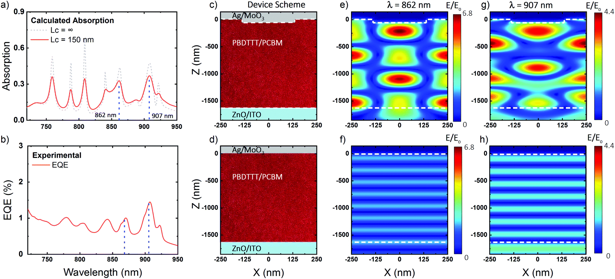 | ||
| Fig. 4 (a) Calculated absorption of the fabricated devices with fully coherent light (grey dashed) and 150 micron coherent light (red). (b) External quantum efficiency measurements for a PBTTT:PC71BM nanostructured photodetector with a lattice parameter of L = 500 nm. Sample scheme for nanostructured and flat devices (c), (d) and calculated electric fields at wavelengths 862 and 907 nm (e), (f) and (g), (h). | ||
2.3 Additional design rules
In this section, we explore the influence of additional geometrical parameters on the performance of the devices. We first start by looking at the thickness of the active layer (Fig. S6 and S7, ESI†). Two main observations can be made. First, the enhanced frequencies are mainly given by the lattice parameter, almost independently of the active layer thickness (in the range considered here). This is a remarkable difference with respect to micro-cavity-based photodetectors.25Second, the optimum active layer thickness in terms of the enhancement factor, arising from the compromise between the optical and electrical properties of the device. Thin active layers (on the order of 100 nm) exhibit high EQEs in the visible but negligible CTS absorption in the NIR. Thicker active layers exhibit enhanced CTS absorption, but often deteriorated electrical response. This is due to the non-uniform charge generation distribution across the film thickness, which implies that the travel path for half of the charges is significantly longer, leading to high recombination probabilities, and finally decreasing the overall electrical response.16 We have found optimum active layer thicknesses of 700 nm for P3HT:PC61BM and of 1600 nm for PBTTT:PC71BM. The optimum thickness is higher for PBTTT because of its higher mobility with respect to P3HT.33
Another important parameter to take into account when designing the nanostructure is the depth of the array of holes imprinted on the active layer. Deeper holes lead to features exhibiting stronger diffraction and thus provide more efficient light trapping. However, if the imprinted holes are too deep, the MoO3 electron blocking layer that is evaporated on top may not form a continuous film, leading to pinholes that disrupt the electrical properties of the device (e.g. unacceptably high dark currents). For this reason, we limited the height of the features in our architecture to 60 nm, avoiding pinhole generation with a complete coverage of the active layer by each of the subsequent layers. This effect is illustrated by comparing devices with different MoO3 layer thicknesses in Fig. S2 (ESI†).
The active layer morphology is often a very important parameter for the performance of organic based diodes.33–36 While a full study of morphological effects on the response of NIR photodiodes goes beyond the scope of this manuscript, we have evaluated the role of thermal annealing on the EQE of the devices. Indeed, we have found that annealing the samples has a significant effect on its performance, increasing its response by 10–20 times (Fig. S8, ESI†).
2.4 Advanced photodiode characterization
In this section, we show the performance of the photonic NIR photodetectors as a function of bias, illumination, time response as well as illustrating the spatial homogeneity of the performance.First, we start by evaluating the photodetectors under reverse V bias to evaluate the charge generation and collection capacity of our nanostructured devices compared to the flat reference samples. The photodetector with the imprinted L = 500 nm structure on the PBTTT:PC71BM active layer presented an increase in EQE from 2% to 7.5% at 907 nm while the reference device still lays below 2% under a 23 V reverse bias (Fig. 5a and b). At this high reverse bias, practically all charges generated are extracted, further improving the charge extraction from CTS. This is translated into a 4 times efficiency increase in our photonically enhanced devices under reverse bias, compared to the unbiased case. The saturation of the charge extraction, upon applying a reverse V bias, occurs much earlier in planar devices (12 V) than in our imprinted devices (28 V) confirming the important difference in charge generation between our nanostructured photodetector and the reference one (Fig. 6a). At high applied bias, the photoresponse of the device is only limited by the absorption of the material, since the bias helps to dissociate charges. It is here where the effect of the improved absorption in the photonic case is most evident.
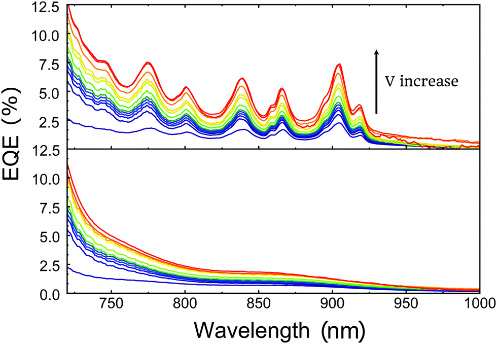 | ||
| Fig. 5 EQE measurements with various reverse V bias from 0 V to 23 V for (a) nanostructured and (b) non-structured (flat) PBTTT:PC71BM photodetectors. | ||
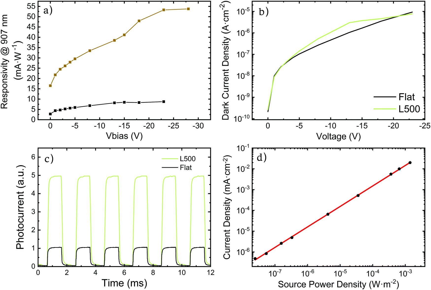 | ||
| Fig. 6 (a) Responsivity at 907 nm for different V bias of L = 500 (nanostructured) and non-structured (flat) PBTTT:PC71BM photodetector. (b) Dark current of both flat and L = 500 nanostructured devices at various reverse V bias. (c) Time dependent normalized photoresponse measurement for both flat and L = 500 nanostructured devices at 0 V bias. (d) Linear dynamic range of PBTTT:PC71BM nanostructured photodetector. | ||
This enhancement can also be observed on the responsivity of the photodetectors, where the L = 500 nm PBTTT:PC71BM device shows a responsivity of 15 mA W−1 in contrast with the 3 mA W−1 for their flat counterpart at 907 nm. (Fig. S9, ESI†). When a reverse V bias is applied the responsivity also increases significantly reaching 54 mA W−1 for the nanostructured devices at 23 V versus the response of 9 mA W−1 of their flat counterparts at the same voltage (Fig. 6a).
While the performance of our OPDs is one order of magnitude lower than that of singlet absorption based OPDs, the values obtained are on the same order of magnitude as other OPDs based on similar strategies, such as the ones reported by Meredith et al.16 Also they exhibit a similar performance on the NIR to previously reported CTS based photodetectors that worked under high reverse V biases of 200 V.21,37
Nanoimprinted and flat devices exhibit similar dark currents, indicating that we successfully avoided pinhole formation and have a good conformal layer deposition (Fig. 6b). Obtained values are around 10 nA cm−2 at 1 V and 1 μA cm−2 at 15 V. We consider this dark current values low considering the large area of photodetection (8 mm2). Taking into account the fact that, especially with solution processing, dark current does not scale up on a linear fashion. That meaning that maintaining low current densities at high areas is much more difficult due to higher probability of having defects on the production of larger devices.
Thanks to these low dark currents, the on/off ratio of our nanostructured photodetectors at 3.5 mW cm2 is around 850 for L = 500 nm at −1 V and 907 nm, being 5.5 times higher than in flat photodetectors (150). These values are comparable to other organic photodiodes, such as those reported by Zhu et al. and Jahnel et al.38,39 For L = 600 nm photodetectors, the on/off ratio decreases down to 15 at a wavelength of 1080 nm and under 1 V of reverse bias, but they still outperform their flat counterparts, with on/off ratios of 3 at the same conditions. Under higher reverse biases the on/off ratio is still consistently superior for the nanostructured devices when compared with their flat reference (Fig. S10, ESI†). While a full frequency response study has not been performed, the transient photocurrent experiments revealed that these devices show rise times on the order of microseconds at 0 V bias, for both nanostructured and flat devices as shown in Fig. 6c. These results show that the nanostructure does not significantly affect the frequency response of the devices.
The response of the nanostructured photodetectors is highly linear as illustrated by the linear dynamic range measurement of the L = 500 structure at 907 nm, which exhibits r2 values of 0.999 over more than 50 dB and a slope of 0.98565, in the whole range available to our set up (Fig. 6d). The fact that the slope is so close to one guarantees a linear response of the photodetector on the given range.
Finally, in order to evaluate the spatial homogeneity of the devices, we fabricated large area devices with patterned areas of 1 cm2 surrounded by flat regions and we performed light beam induced photocurrent (LBIC) mapping. For this, we used a PBTTT:PC71BM sample which included areas structured with three different lattice parameters. The photocurrent maps in Fig. 7 clearly demonstrate that the photocurrent is enhanced where the active layer has been structured. Moreover, the cm squared areas are relatively homogeneous, with the modulations in photocurrent intensity arising from small thickness variations produced during the blade coating of an entire microscope slide.
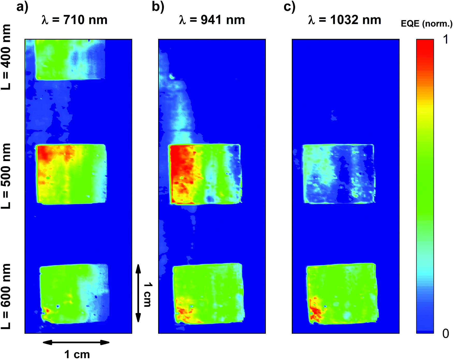 | ||
| Fig. 7 Light beam induced photocurrent (LBIC) maps of a large area continuous back electrode photodetector, at 3 different excitation wavelengths: (a) 710 nm, (b) 941 nm and (c) 1032 nm, with 3 different nanostructured zones. From top to bottom: L = 400, L = 500 and L = 600. | ||
The inspection of the devices at three different wavelength excitations showed how the absorption of the CTS depended greatly on the lattice parameter, in agreement with the EQE data (Fig. 3). When excited with a wavelength of 710 nm, all three patterns offer similar responses because they all provide diffraction at these wavelengths, where the singlet tail absorption is still present (Fig. 7a). Although no significant difference is observed between the three patterns, they all outperform the flat non-patterned regions that can be seen in between the patterns, revealing the importance of the nanostructuration. When the excitation wavelength is set to 941 nm, where there is no contribution of the singlet tail absorption, only CTS absorption, the difference between the three fabricated structures becomes more relevant (Fig. 7b). At this wavelength, the pattern of L = 400 nm does not provide diffraction orders capable to enhance the absorption the CTS and produce a noticeable photocurrent, so its response is equal to the flat zones.
Meanwhile, regions with L = 600 nm and 500 nm still show good photocurrents, being the last one the optimum for this wavelength, as studied before with the spectral EQE. Finally, at 1031 nm, only the region patterned with the 600 nm lattice parameter offers good enhancement with respect to the planar reference.
Interestingly, the response for each lattice parameter presents a series of peaks. For a given wavelength, each effective pixel has a different response. If each pixel is calibrated using the EQE data, one could think of a spectrometer based on three pixels, emulating the RGB strategy, but for the NIR. Fig. 7 can be considered, therefore, as an artificial NIR eye.
3. Conclusions
We report a new organic BHJ based photodetector architecture that is capable of detecting light at wavelengths significantly below the bandgap of its components. This was achieved by boosting the absorption of the long CTS absorption tail present in P3HT:PC61BM and PBTTT:PC71BM blends. Their CTS absorption was enhanced by incorporating a photonic architecture within the device via the nanostructuration of the active layer. Both the active layer and the patterning are carried out using roll to roll compatible and highly scalable techniques. The wavelength at which the photodetectors response is enhanced proved to be quite insensitive to thickness variations, offering appealing fabrication tolerances.Furthermore, the used polymers and small molecules are inexpensive and easy to produce, making them ideal for large scale production. The performance of the photodetectors was tested through several techniques, showing that our nanostructured OPDs are significantly superior than flat OPDs on the NIR thanks to our strategy to enhance the CTS absorption. In addition, we demonstrated that different nanostructuration configurations enhance the response of the photodetectors at different wavelengths, rendering any of our devices wavelength tunable within a wide region on the NIR. In summary, we have developed wavelength tunable NIR photodetectors exploiting the CTS absorption, which opens new opportunities for the operation of organic based devices beyond their bandgaps.
4. Experimental section
4.1 Materials and devices
Poly(3-hexylthiophene-2,5-diyl) (P3HT) (99.995%) (regioregular 95%, average Mn 54![[thin space (1/6-em)]](https://www.rsc.org/images/entities/char_2009.gif) 000–75000) was bought from Sigma Aldrich. Phenyl-C61-butyric acid methyl ester (PC61BM) (>99.5%) and [6,6]-phenyl C71 butyric acid methyl ester (PC71BM) (>99%), were purchased from OSSILA.
000–75000) was bought from Sigma Aldrich. Phenyl-C61-butyric acid methyl ester (PC61BM) (>99.5%) and [6,6]-phenyl C71 butyric acid methyl ester (PC71BM) (>99%), were purchased from OSSILA.
We have manufactured two main types of photodetectors; either with the pixelated substrates or with a continuous ITO back electrode, to be used in the EQE and LBIC measurements respectively.
On top of a pre-cleaned ITO covered glass substrate, we have deposited the ZnO electron transport layer from a nanoparticle solution (Avantama N-10) via Blade coating (Zehntner ZAA 2300). The parameters we have used are the following: droplet volume 50 μl, blade gap 50 μm, blade temperature 40 °C and speed 5 mm s−1. After the layer had been deposited we anneal it at 100 °C to fully dry and improve crystallinity. This procedure was repeated four times. Each time the deposition was performed on the opposite direction to the prior deposition. After this step, we proceeded to deposit the active layer, for the two different mixtures, the P3HT:PC61BM (1:0.8) and the PBTTT:PC71BM (1:4) (30 mg ml−1) which had been dissolved in a mixture of chlorobenzene and dichlorobenzene (1:1). It was deposited via blade coating, with the following parameters: droplet volume 50 μl, blade gap 50 μm, blade temperature 90 °C and speed 84 mm s−1. The active layer was also deposited four times sequentially on opposite directions each time. Afterwards, the active layer was nanostructured via Nanoimprinting lithography, where we pressed with a prepatterned PDMS stamp at 4 bars while heating at 135 °C under vacuum conditions. This procedure was done with a Nanoimprinting Lithography setup (CNI v2.1 from NIL technologies). Afterwards we gently and slowly pulled the PDMS stamp away from the substrate, revealing the nanostructured surface that was visibly iridescent. On top of the active layer we deposited a layer of 10 nm of MoO3 by thermal evaporation at a rate of 0.1 nm s−1. And then we evaporated a back electrode of 200 nm of silver at an initial rate of 0.1 nm s−1 until 40 nm and then at a rate of 0.3 nm s−1. Later on we proceed to encapsulate the samples with a glass coverslip and epoxy resin. Finally, we annealed the samples at 135 °C during 20 minutes.
4.2 Organic photodetector characterization
Conflicts of interest
The authors declare no conflicts of interest.Acknowledgements
We greatly acknowledge financial support from the Ministerio de Ciencia, Innovación y Universidades MICINN with projects PGC2018-095411-B-I00, MAT2016-79053-P and MAT2015-70850-P and the “Severo Ochoa” excellence program SEV-2015-0496; Generalitat de Catalunya program AGAUR 2017-SGR-00488; and the European Research Council (ERC) under the European Union's Horizon 2020 research and innovation programme (grants no. CoG648901 and StG637116). P. M. acknowledges financial support from an FPI contract (2017) of the MICINN (Spain) cofounded by the ESF. M. G. R. acknowledges financial support from an FPU grant (no. 16/02631) (2017) of the MICINN (Spain). M. G. R. and P. M. B. acknowledge the departments of Physics, Chemistry and Geology of the Autonomous University of Barcelona (UAB) as coordinators of the PhD programme in Materials Science. We acknowledge support of the publication fee by the CSIC Open Access Publication Support Initiative through its Unit of Information Resources for Research (URICI).References
- X. Gong, M. Tong, Y. Xia, W. Cai, J. S. Moon, Y. Cao, G. Yu, C. L. Shieh, B. Nilsson and A. J. Heeger, Science, 2009, 325, 1665–1667 CrossRef CAS PubMed.
- H. Wang and D. H. Kim, Chem. Soc. Rev., 2017, 46, 5204–5236 RSC.
- R. J. Bruening, Appl. Opt., 1987, 26, 1051–1057 CrossRef CAS PubMed.
- L. R. Canfield, R. E. Vest, T. N. Woods and R. S. Korde, Proc. SPIE, 1994, 2282, 31–38 CrossRef CAS.
- R. R. Søndergaard, M. Hösel and F. C. Krebs, J. Polym. Sci., Part B: Polym. Phys., 2013, 51, 16–34 CrossRef.
- C. Brabec (Linz) and E. Hauch (Erlangen), US Pat., 7476278 B2, 2009 Search PubMed.
- S. Tong, J. Yuan, C. Zhang, C. Wang, B. Liu, J. Shen, H. Xia, Y. Zou, H. Xie, J. Sun, S. Xiao, J. He, Y. Gao and J. Yang, npj Flexible Electron., 2018, 2, 1–8 CrossRef CAS.
- T. Yokota, P. Zalar, M. Kaltenbrunner, H. Jinno, N. Matsuhisa, H. Kitanosako, Y. Tachibana, W. Yukita, M. Koizumi and T. Someya, Sci. Adv., 2016, 2, 1–9 Search PubMed.
- Y. Li, Acc. Chem. Res., 2012, 45, 723–733 CrossRef CAS PubMed.
- M. R. Antognazza, U. Scherf, P. Monti and G. Lanzani, Appl. Phys. Lett., 2007, 90, 21–24 CrossRef.
- N. Strobel, N. Droseros, W. Köntges, M. Seiberlich, M. Pietsch, S. Schlisske, F. Lindheimer, R. R. Schröder, U. Lemmer, M. Pfannmöller, N. Banerji and G. Hernandez-Sosa, Adv. Mater., 2020, 32, 1908258 CrossRef CAS PubMed.
- L. Dou, Y. Liu, Z. Hong, G. Li and Y. Yang, Chem. Rev., 2015, 115, 12633–12665 CrossRef CAS PubMed.
- X. Liu, Y. Lin, Y. Liao, J. Wu and Y. Zheng, J. Mater. Chem. C, 2018, 6, 3499–3513 RSC.
- C. Battaglia, C. M. Hsu, K. Söderström, J. Escarré, F. J. Haug, M. Charrière, M. Boccard, M. Despeisse, D. T. L. Alexander, M. Cantoni, Y. Cui and C. Ballif, ACS Nano, 2012, 6, 2790–2797 CrossRef CAS PubMed.
- G. Konstantatos and E. H. Sargent, Nat. Nanotechnol., 2010, 5, 391–400 CrossRef CAS PubMed.
- A. Armin, R. D. Jansen-Van Vuuren, N. Kopidakis, P. L. Burn and P. Meredith, Nat. Commun., 2015, 6, 6343 CrossRef CAS PubMed.
- E. T. Hoke, K. Vandewal, J. A. Bartelt, W. R. Mateker, J. D. Douglas, R. Noriega, K. R. Graham, J. M. J. Fréchet, A. Salleo and M. D. Mcgehee, Adv. Energy Mater., 2013, 3, 220–230 CrossRef CAS.
- K. Vandewal, K. Tvingstedt, A. Gadisa, O. Inganäs and J. V. Manca, Nat. Mater., 2009, 8, 904–909 CrossRef CAS PubMed.
- C. Deibel, T. Strobel and V. Dyakonov, Adv. Mater., 2010, 22, 4097–4111 CrossRef CAS PubMed.
- P. Panda, D. Veldman, J. Sweelssen, J. J. A. M. Bastiaansen, B. M. W. Langeveld-Voss and S. C. J. Meskers, J. Phys. Chem. B, 2007, 111, 5076–5081 CrossRef CAS PubMed.
- C. M. Yang, P. Y. Tsai, S. F. Horng, K. C. Lee, S. R. Tzeng, H. F. Meng, J. T. Shy and C. F. Shu, Appl. Phys. Lett., 2008, 92, 7–10 Search PubMed.
- H. Chalabi, D. Schoen and M. L. Brongersma, Nano Lett., 2014, 14, 1374–1380 CrossRef CAS PubMed.
- S. Li, D. Xue, W. Xu, Y. Feng, J. Wang, G. Zhang, X. Meng, C. Wang, Y. Song and C. Shu, J. Mater. Chem. C, 2014, 2, 1500–1504 RSC.
- A. G. MacEdo, F. Zanetti, A. Mikowski, J. C. Hummelen, C. M. Lepienski, M. G. E. Da Luz and L. S. Roman, J. Appl. Phys., 2008, 104, 033714 CrossRef.
- Z. Tang, Z. Ma, A. Sánchez-Díaz, S. Ullbrich, Y. Liu, B. Siegmund, A. Mischok, K. Leo, M. Campoy-Quiles, W. Li and K. Vandewal, Adv. Mater., 2017, 29, 1–8 Search PubMed.
- E. Yablonovitch, J. Mod. Opt., 1994, 41, 173–194 CrossRef CAS.
- S. W. Baek, P. Molet, M. J. Choi, M. Biondi, O. Ouellette, J. Fan, S. Hoogland, F. P. García de Arquer, A. Mihi and E. H. Sargent, Adv. Mater., 2019, 31, 1901745 CrossRef PubMed.
- P. Shen, G. Wang, B. Kang, W. Guo and L. Shen, ACS Appl. Mater. Interfaces, 2018, 10, 6513–6520 CrossRef CAS PubMed.
- L. Xu, C. Aumaitre, Y. Kervella, G. Lapertot, C. Rodríguez-Seco, E. Palomares, R. Demadrille and P. Reiss, Adv. Funct. Mater., 2018, 28, 1706291 CrossRef.
- M. Mariano, G. Kozyreff, L. G. Gerling, P. Romero-Gomez, J. Puigdollers, J. Bravo-Abad and J. Martorell, Light Sci. Appl., 2016, 5, e16216–e16216 CrossRef CAS PubMed.
- Y. Xia and G. M. Whitesides, Angew. Chem., Int. Ed., 1998, 37, 550–575 CrossRef CAS PubMed.
- Y. Xia, J. A. Rogers, K. E. Paul and G. M. Whitesides, Chem. Rev., 1999, 99, 1823–1848 CrossRef CAS PubMed.
- I. McCulloch, M. Heeney, C. Bailey, K. Genevicius, I. MacDonald, M. Shkunov, D. Sparrowe, S. Tierney, R. Wagner, W. Zhang, M. L. Chabinyc, R. J. Kline, M. D. McGehee and M. F. Toney, Nat. Mater., 2006, 5, 328–333 CrossRef CAS PubMed.
- I. C. Ghosekar and G. C. Patil, Microelectron. Eng., 2020, 221, 111195 CrossRef.
- J. Munshi and G. Balasubramanian, Soft Mater., 2020, 1–14 Search PubMed.
- W. Zhang, H. Shen, B. W. Guralnick, B. J. Kirby, N. A. Nguyen, R. Remy, C. F. Majkrzak and M. E. Mackay, Sol. Energy Mater. Sol. Cells, 2016, 155, 387–396 CrossRef CAS.
- Y. Yao, Y. Liang, V. Shrotriya, S. Xiao, L. Yu and Y. Yang, Adv. Mater., 2007, 19, 3979–3983 CrossRef CAS.
- H. L. Zhu, W. C. H. Choy, W. E. I. Sha and X. Ren, Adv. Opt. Mater., 2014, 2, 1082–1089 CrossRef CAS.
- M. Jahnel, M. Thomschke, S. Ullbrich, K. Fehse, J. D. An, H. Park, K. Leo, C. Im and V. Kirchhoff, Microelectron. Eng., 2016, 152, 20–25 CrossRef CAS.
Footnote |
| † Electronic supplementary information (ESI) available: Theoretical photonic analysis, and supplementary figures. See DOI: 10.1039/d0tc02295k |
| This journal is © The Royal Society of Chemistry 2020 |