
 Open Access Article
 This Open Access Article is licensed under a
 Creative Commons Attribution 3.0 Unported Licence
Epitaxial GaN using Ga(NMe2)3 and NH3 plasma by atomic layer deposition†
Polla
Rouf
 *a,
Nathan J.
O’Brien
a,
Sydney C.
Buttera
b,
Ivan
Martinovic
a,
Babak
Bakhit
a,
Erik
Martinsson
a,
Justinas
Palisaitis
a,
Chih-Wei
Hsu
a and
Henrik
Pedersen
a
*a,
Nathan J.
O’Brien
a,
Sydney C.
Buttera
b,
Ivan
Martinovic
a,
Babak
Bakhit
a,
Erik
Martinsson
a,
Justinas
Palisaitis
a,
Chih-Wei
Hsu
a and
Henrik
Pedersen
a
aDepartment of Physics, Chemistry and Biology, Linköping University, SE-58183 Linköping, Sweden. E-mail: polla.rouf@liu.se
bDepartment of Chemistry, Carleton University, 1125 Colonel By Drive, Ottawa, Ontario K1S 5B6, Canada
First published on 25th May 2020
Abstract
Low temperature deposition of high-quality epitaxial GaN is crucial for its integration in electronic applications. Chemical vapor deposition at approximately 800 °C using SiC with an AlN buffer layer or nitridized sapphire as substrate is used to facilitate the GaN growth. Here, we present a low temperature atomic layer deposition (ALD) process using tris(dimethylamido)gallium(III) with NH3 plasma. The ALD process shows self-limiting behaviour between 130–250 °C with a growth rate of 1.4 Å per cycle. The GaN films produced were crystalline on Si (100) at all deposition temperatures with a near stochiometric Ga/N ratio with low carbon and oxygen impurities. When GaN was deposited on 4H-SiC, the films grew epitaxially without the need for an AlN buffer layer, which has never been reported before. The bandgap of the GaN films was measured to be ∼3.42 eV and the Fermi level showed that the GaN was unintentionally n-type doped. This study shows the potential of ALD for GaN-based electronic devices.
Introduction
Gallium nitride (GaN) is a key material in microelectronics based on the group 13-nitride materials. This is due to its favourable properties of wide and direct bandgap, high thermal stability, high breakdown field and good electron mobility.1–4 In high frequency electronics, GaN films are preferably deposited on SiC due to its high thermal conductivity.5 However, it is difficult to deposit GaN directly on SiC by CVD due to poor wetting of GaN on SiC.6 Therefore, an AlN buffer layer is used to facilitate GaN growth.7–9 Currently, thin films of electronic grade epitaxial GaN are deposited by chemical vapor deposition (CVD) processes using trimethylgallium (TMG) and ammonia (NH3) at temperatures between 800–1000 °C.10 The high deposition temperatures are required to obtain highly crystalline films but also to overcome the poorly suited precursor combination of TMG and NH3, which leads to high N/Ga precursor ratios of 103. CVD also hinder the deposition of highly conformal GaN films on topographically complex surfaces and on temperature sensitive materials. To meet these challenges, the low temperature time-resolved CVD route known as atomic layer deposition (ALD) has been studied for GaN. Deposition of GaN by ALD has been achieved using TMG or triethylgallium (TEG) with N2/H2 plasma,11 NH3 plasma11,12 or thermally with NH3.13 However, these processes suffer non-stoichiometric Ga/N ratios and high carbon and oxygen impurities. Additionally, thermal ALD with TMG and NH3 requires deposition temperatures of 400 °C, which is relatively high for an ALD process.13 Similar issues has been reported for ALD of GaN using TEG, were impurities of C and O was the primary issue.14,15 ALD routes using GaCl and GaCl3 together with NH3 deposited at high temperature (>400 °C) have also been investigated, but render films with Cl impurities.16,17The disadvantage of TMG and TEG for ALD of GaN is their strong M–C bonds, which makes it difficult to remove all of their ligands from the deposited precursor at low temperatures.18 Amides (M–NR2) have more reactive and desirable M–N bonds, which would improve the surface chemistry during the NH3 precursor pulse. Herein, we report low temperature deposition of GaN using tris(dimethylamido)gallium(III), Ga(N(CH3)2)31, with NH3 plasma by ALD. Precursor 1 has been previously used for ALD of Ga2O319,20 and Ga2S321 and CVD of GaN,22 but not for ALD of GaN. Notably, all previous reports using 1 has resulted in amorphous films at all deposition temperatures.19,21,22 We show that 1 displayed self-limiting behaviour in a temperature range from 130–250 °C on Si (100). Deposition of GaN on 4H-SiC(0001) rendered epitaxial films with near stochiometric composition and very low impurity levels of carbon and oxygen. To the best of our knowledge, this is the first report of GaN grown epitaxially directly on SiC substrate.
Experimental details
Precursor synthesis
The reaction and manipulations were carried out under a N2 atmosphere on a Schlenk line using Schlenk air-free techniques and in a Glovebox-Systemtechnik dry box. All anhydrous solvents were purchased from Sigma-Aldrich™ and further dried with 4 Å molecular sieves. All NMR spectra were measured with an Oxford Varian 300 spectrometer. Solvents peaks were used as an internal standard for the 1H NMR (300 MHz) spectrum. The melting point was determined in a capillary sealed under N2 with a Stuart® SMP10 melting point apparatus and is uncorrected. GaCl3 (99.99%) was purchased from ACROS-Organics™ and lithium dimethylamide (95%) from Sigma-Aldrich™, and both were used without further purification.Synthesis of tris(dimethylamido)gallium(III) dimer (1)
Tris(dimethylamido)gallium(III) dimer 1 was synthesised using the literature procedure (Fig. 1).23 A room temperature suspension of lithium dimethylamide (5.2 g, 102 mmol) in n-hexanes (150 mL) was slowly added to a –20 °C solution of GaCl3 (6.0 g, 34.1 mmol) in n-hexanes (100 mL) via cannula and the mixture was stirred at this temperature for 1 h. The reaction was slowly warmed to room temperature and stirred for a further 16 h. The reaction mixture was filtered through a pad of Celite and concentrated under reduced pressure to give a solid. The solid was purified by recrystallisation from Et2O at −35 °C to give the compound 1 as a solid (4.61 g, 63%).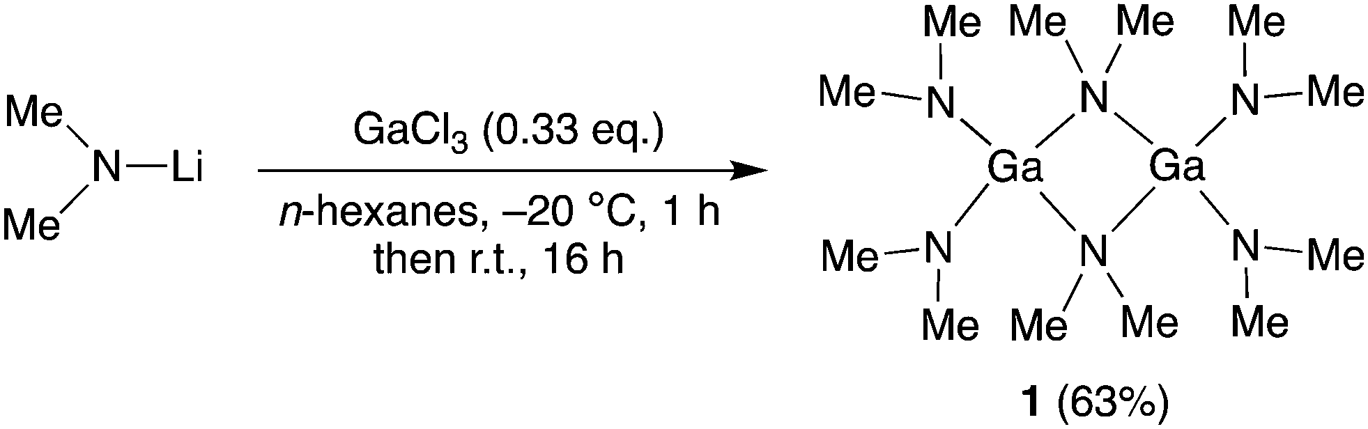 | ||
| Fig. 1 Synthesis of tris(dimethylamido)gallium(III) 1. | ||
1: Colourless solid, m.p. 101–104 °C. 1H NMR (300 MHz, C6D6) δ 2.34 (s, 12H, μ-NMe2), 2.68 (24H, μ-NMe2).
Thermogravimetric analysis and differential scanning calorimetry
The volatilization curve was collected using a TA Instruments thermogravimetric analysis Q500 tool. The ramp experiment of 1 was undertaken inside a N2 glovebox in a tared aluminum pan loaded with 18 mg of 1. The furnace was heated at a rate of 10 °C min−1 to 400 °C with a maintained N2 flow rate of 60 sccm. The differential scanning calorimetry (DSC) measurement for 1 was performed on a TA Instruments DSC Q10 tool. The sample was prepared in a sealed aluminum pan in a N2 filled glovebox and weighed approximately 0.2 mg. The experiments heated the sample of 1 and a blank reference pan at a rate of 10 °C min−1 to 400 °C.Film deposition
The films were deposited in a Picosun R-200 ALD system equipped with a Litmas Remote Inductively Coupled Plasma Source. The system used a base pressure of 400 Pa with continuous N2 (99.999%, further purified with a getter filter to remove moisture) flow through the deposition chamber. The Si (100) and 4H-SiC (0002) substrates were cut into 1.5 × 1.5 cm pieces and Si (100) was used without further cleaning whilst 4H-SiC was cleaned with RCA-1 (solution of 1 part H2O2 (30%), 1 part NH3 (25%) and 5 parts H2O) and RCA-2 (1 part H2O2 (30%), 1 part HCl (37%) and 6 parts H2O)24 solutions to remove organic and inorganic contaminants on the surface prior to deposition. The substrates were loaded into the reactor onto a heated substrate holder and the system was heated to 450 °C for 120 minutes before each run with a continuous N2 flow (300 sccm) to minimize the oxygen content in the chamber. Approximately 500 mg of 1 was placed in a glass vial in a stainless-steel bubbler without a dip-tube for incoming carrier gas. The temperature of the bubbler was set at 120 °C with a N2 flow of 100 sccm to aid transporting the precursor vapor into the deposition chamber. A 10 s N2 purge was used after the pulse of 1. The NH3 (AGA/Linde, 99.999%) plasma used as the nitrogen source was an Ar (99.999%, further purified with a getter filter to remove moisture)/NH3 (100/75 sccm) mixture, ignited using a plasma power of 2800 W. These plasma parameters was previously investigated to be optimal for our reactor and deposition of nitrides.25 A plasma pulse of 9 s followed by a 10 s purge was used with the above parameters unless otherwise stated. The thickness of the GaN film was 70 nm unless otherwise stated.Characterisation
The crystallinity of deposited films was studied using a PANalytical EMPYREAN MRD XRD with a Cu-anode X-ray tube and 5-axis (x-y-z-v-u) sample stage both in θ–2θ and grazing incidence (GIXRD) configuration. Strain in the films was estimated from the GIXRD measurement for each diffraction peak values of sin2ψ and ε was obtained using the software X’Pert Stress. PANalytical X’Pert PRO with a Cu-anode tube and Bragg–Brentano HD optics was used for θ–2θ measurement and in X-ray Reflectivity (XRR) mode to measure the film thickness. The software PANalytical X’Pert reflectivity was used to fit the XRR data using a two-layer model of the GaN film and the substrate (GaN/substrate). A LEO 1550 Scanning electron microscope (SEM) with an acceleration energy of 10–20 kV was used to characterise the morphology of the film. The film composition and chemical bonding environments of the atoms in the film were characterized with a Kratos AXIS Ultra DLD X-ray photoelectron spectroscopy (XPS) equipped with Ar (0.5 keV) sputtering source. CasaXPS software was used to evaluate the data. Gaussian–Laurentius functions and Shirley background were used to fit the experimental XPS data. The absorption spectroscopy measurements were conducted using a custom fibre optical setup consisting of a light source (Ocean Optics DH-2000-BAL), a detector (Avantes AvaSpec-Dual) and a bifurcated optical fibre (Ocean Optics BIFBORO-2-1000). An absorption spectrum for the GaN film was collected using a custom software based on LabView (National Instruments) with a Si (100) substrate used as a reference.Elemental composition of the films was obtained using Rutherford backscattering spectrometry (RBS) and time-of-flight elastic recoil detection analyses (ToF-ERDA). The measurements were carried out in a 5-MV NEC-5SDH-2 pelletron tandem accelerator. 2 MeV 4He+ ions were employed for RBS and detected in a scattering angle of 170°. Two different geometries, azimuth angle 5° + tilt angle 2° and azimuth angle 40° + tilt angle 2°, were chosen in order to minimize channelling effects. In addition, more suppression of the probable channelling effects was undertaken by multiple small random-angular movements around the equilibrium angles within a range of 2°. RBS spectra were fitted by SIMNRA 7.02 code26 with an ∼1% statistic uncertainty to determine elemental compositions. Recoils, in ToF-ERDA, were detected at 45° angle between the primary beam and a ToF-E detector telescope in a gas ionization chamber (GIC) using a 36 MeV 127I8+ beam incident at 67.5° with respect to the sample surface normal. The ToF-E detector telescope consisted of two circular carbon foils with 8 and 5 μg cm−2 thicknesses, 6 mm radius, a 0.05 msr solid angle (ΔΩ), and a flight distance of 425 mm between the foils. Utilizing a ToF-GIC setup provides the system with a good energy resolution and enhanced ion species separation in terms of mass and energy.27 Average elemental compositions were also obtained from ToF-ERDA time-energy coincidence spectra using two different software packages, CONTES28 and Potku.29 Systematic uncertainties of the experiment, discussed in more detail elsewhere30 in particular for light elements, were estimated to be a maximum of 5–10%, whereas statistic uncertainties arisen from the number of experimental counts were <2.3%. However, the relative elemental concentrations were obtained with higher accuracy.31,32 The stopping power data required for both RBS and ERDA simulations was retrieved from SRIM2013 code.33
Cross-sectional transmission electron microscope (TEM) samples were prepared by the traditional sandwich approach, which includes sample cutting, gluing, polishing and ion milling. A Gatan Precision Ion Polishing System Model 691 operated at 5 kV and 40 mA, with an Ar ion source, was used to make the samples electron transparent. Scanning transmission electron microscopy (STEM) and selective area electron diffraction (SAED) characterization were performed using the Linköping double Cs corrected FEI Titan3 60–300 operated at 300 kV.
Results and discussion
Tris(dimethylamido)gallium(III) dimer 1 has been previously used in ALD studies,19–21 however its thermal properties have not been reported as far as we know. Thermogravimetric analysis (TGA) showed 1 evaporated in a single step from 140–230 °C, with only 5% of residual mass (Fig. 2a). The 1 torr vapour pressure of 1 was shown to occur at 109 ± 5 °C its ΔH of vaporization was 59.5 kJ mol−1 (Fig. S1, ESI†). Differential scanning calorimetry (DSC) showed an endothermic peak at 103 °C and a small broad exothermic event with a peak at 193 °C (Fig. 2b). The endothermic event peak corresponds to the melting point of 1 (103–106 °C), which matches our observed DSC value, whilst the exothermic event indicates high temperature decomposition. These results show that 1 is a thermally stable precursor and has favourable properties for use in ALD of GaN.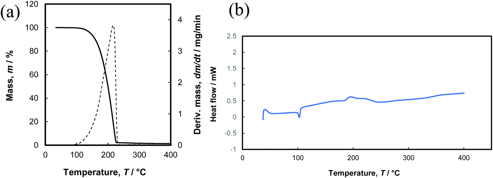 | ||
| Fig. 2 (a) Thermogravimetric analysis and (b) differential scanning calorimetry of 1. | ||
To study if 1 could be used in self-limiting deposition of GaN, ALD experiments on Si (100) substrates were undertaken using varied pulse times for 1 and NH3 plasma whilst the temperature was maintained at 200 °C. The GaN growth per cycle (GPC) saturates at 1.4 Å per cycle when the pulse time of 1 is 4 s or longer (Fig. 3a). The GPC saturates at the same value for NH3 plasma when pulse times of 6 s or longer were used. This is indicative of a self-limiting growth and surface chemistry between 1 and NH3 plasma. The growth per cycle was constant between 130–250 °C when using a 4 s pulse time for 1 and 9 s NH3 plasma pulse time (Fig. 3b). As the bubbler temperature was set to 120 °C, lower deposition temperature was not conducted due to the risk of condensation of 1 on the substrate. Reactor temperatures of ≥250 °C resulted in a decreased GPC, indicating desorption of the precursor from the substrate.
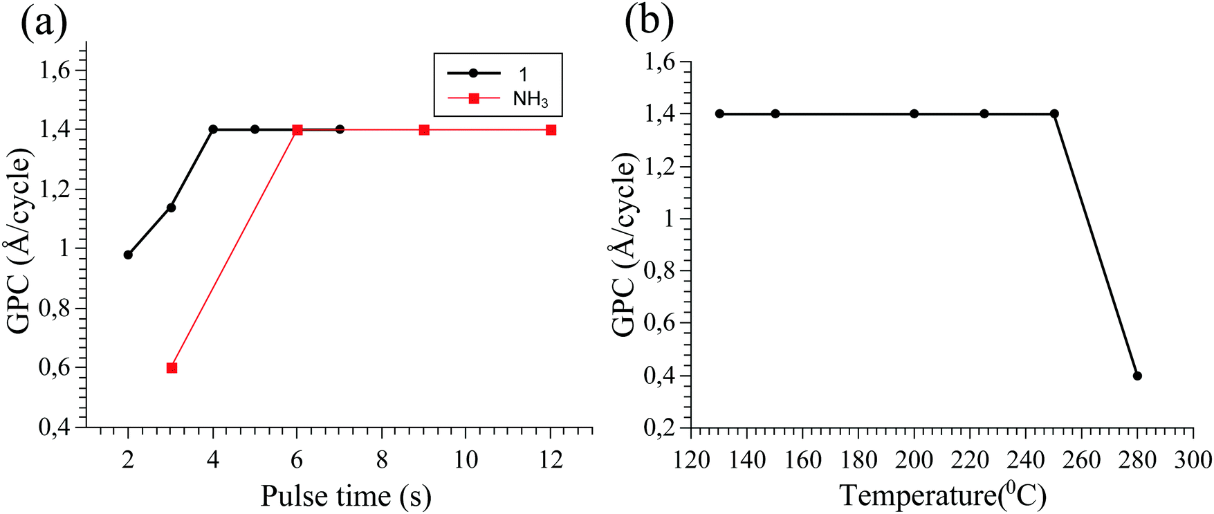 | ||
| Fig. 3 (a) The saturation curves of 1 (black circles) with 9 s NH3 plasma pulse and NH3 plasma (red squares) with 4 s pulse of 1 deposited at 200 °C. (b) The GPC dependence on temperature using 9 s pulses of NH3 plasma and 4 s pulses of 1. | ||
This GPC is roughly 3–5 times that of previous reports of GaN plasma processes with TMG/TEG.11,12,14 It can be noted here that the wurtzite GaN lattice has a c lattice constant of 5.182 Å. To obtain such a unit cell, three monolayers are required (Ga source, N source followed by Ga source) which corresponds to 1.5 ALD cycles and therefore the theoretical maximum growth per cycle is approximately 3.45 Å per cycle. The growth of 1.4 Å per cycle obtained with the M–N bonded precursor 1 is lower than the theoretical growth making it reasonable despite its higher growth rate compared to other GaN processes.
The films deposited in the temperature window with constant GPC rendered crystalline GaN with a preferred (002) orientation on Si (100) (Fig. 4a). The intensity of the XRD peaks, which is especially clear from the GIXRD measurements (Fig. 4b), increases with higher deposition temperature suggesting that film crystallinity increases with temperature. The (002) plane is present in both the θ–2θ XRD and the GIXRD indicating that grains tilted with respect to the substrate normal are present in the film. The stress and strain in the 70 nm GaN films were estimated from the GIXRD measurement by a ε–sin2ψ plot (Fig. 4c). The positive slope of the fitted line to the plotted data is indicative of tensile strain of the film. The strain was obtained from the slope (7475.61 ppm) and gives a value of 0.00747561. This corresponds to roughly 0.75% of tensile strain. To calculate the stress in the film, Young's modulus (E) and Poisson's ratio (v) for GaN was used (eqn (1)).
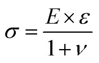 | (1) |
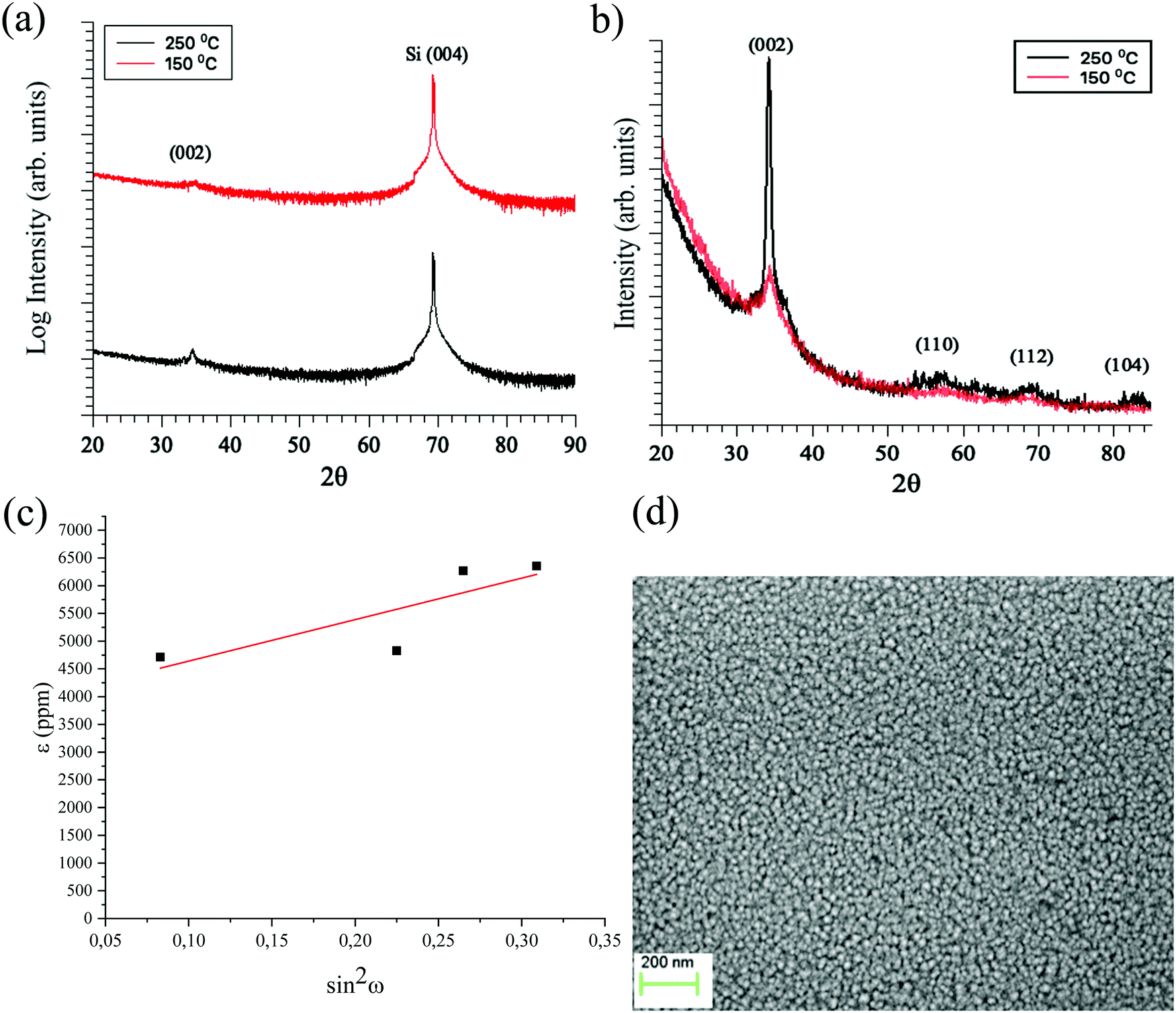 | ||
| Fig. 4 (a) XRD of the films on Si (100) showing GaN (002) peak deposited at 150 °C (red line) and 250 °C (black line) with 9 s NH3 plasma pulse and 4 s pulse of 1 with a thickness of approximately 70 nm. (b) GIXRD of the films on Si (100) with 4 s pulse of 1, 9 s NH3 plasma pulse deposited at 150 °C (red line) and 250 °C (black line) showing GaN (002) peak with a thickness of approximately 70 nm. (c) ε–sin2ψ plot from GIXRD measurement on Si (100) with 4 s of 1 and 9 s NH3 plasma deposited at 250 °C with a thickness of approximately 70 nm. (d) Top-view SEM of the film on Si (100) with 4 s pulse of 1 and 9 s NH3 pulse deposited at 250 °C with a thickness of approximately 70 nm. | ||
The Youngs's modulus and Poisson's ratio of GaN have been determined from previous studies to be 325.3 GPa and 0.25, respectively.34 This gives a tensile stress of about 1.95 GPa for the GaN thin film on a Si substrate. Tensile strain and stress in the GaN film is expected due to the large difference in lattice constant and crystal structure of cubic Si to hexagonal GaN.
Top-view SEM analysis showed that the films deposited at 250 °C is composed of many small crystalline grains with little variation in grain size (Fig. 4d). The little variation in grain size indicates that the film grows in a layer-by-layer fashion without any observable secondary nucleation.
The chemical bonding environment and atomic composition in the GaN films deposited at 250 °C were analysed by XPS (Fig. 5). High resolution XPS spectra were used to analyse the chemical environment of the Ga 2p3/2 and N 1s regions. Two peaks were used to obtain a good fit for the Ga 2p3/2 at 1117.5 eV and 1119.4 eV, which were attributed to Ga–N and Ga–O bonds, respectively (Fig. 5a). Three peaks were used to fit the N 1s at 397.1 eV, 394.8 eV and 392.7 eV, which were assigned to N–Ga and two Ga Auger peaks, respectively (Fig. 5b). This is in accordance with previous XPS measurements on GaN thin films.11,13,35–37 After sputter cleaning the film surface, XPS measurements gave an initial overall composition of 25.0 at% Ga, 74.5 at% N, 0.5 at% O with no detectable C. It should be noted that the N 1s peak overlaps with Ga Auger peaks, which results in a broad N 1s peak and an overestimate of the N content. To obtain the Ga/N ratio in the film without Ga Auger interference, the Auger peaks were subtracted from the contribution to the N content. The N–Ga peak contribution is 33% of the overall N content, which gives 24.6 at% of N that is attributed to the actual N content of the film. This gives a corrected Ga/N ratio of 1.02, which is close to stochiometric GaN. The high resolution XPS peak of Ga 2p3/2 can be fitted with contributions from Ga–N and Ga–O bonds while the high resolution XPS N 1s peak cannot be fitted with a N–O peak, suggesting that all oxygen in the film is bonded to Ga. If oxygen is subtracted from Ga 2p3/2 spectra and only the Ga–N and N–Ga bonds are considered, a near stoichiometric Ga/N ratio of 0.99 is obtained. To investigate if the subtraction of the Ga Auger peaks from the N 1s XPS region is a sound strategy, RBS combined with ERDA was conducted on the GaN film. The RBS/ERDA measurement showed that the GaN film contained 45.7 at% Ga, 47.2 at% N, 2.8 at% C, 3.1 at% O and 1.2 at% H giving a Ga/N ratio of 0.97, which indicates a slightly under-stochiometric film composition. This shows that even when subtracting the Ga Auger peak from the N 1s XPS region, the film composition and Ga/N ratio is not reliable using XPS and other techniques are required to determine an accurate atomic content. In addition, C impurities were not detected by XPS after clean sputtering whilst RBS/ERDA showed C present in the film, showing the latter is preferred for detection of impurities. In addition, sputtering was used in the XPS measurement, which could cause preferential sputtering and change the composition and impurity levels in the film. Nonetheless, XPS is highly important for accessing the chemical environment of each element.
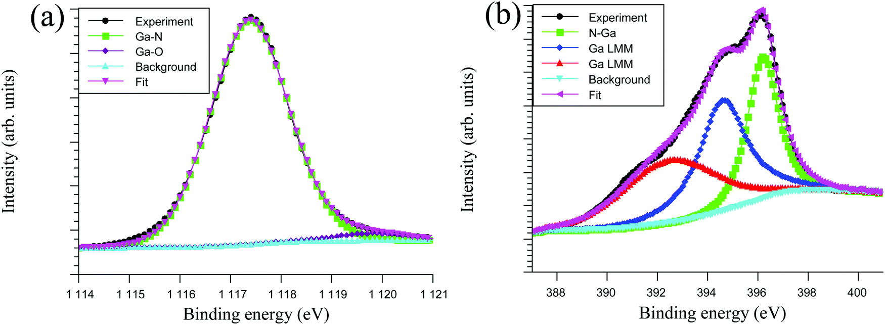 | ||
| Fig. 5 HR-XPS of Ga 2p (a) and N 1s (b) with 4 s of 1 and 9 s NH3 plasma pulse deposited at 250 °C with a thickness of 70 nm. | ||
An absorption measurement was conducted on the GaN film and the data was used to construct a Tauc plot to calculate the bandgap. The optical bandgap for a direct bandgap material is expressed by eqn (2). Extrapolating the linear part in the Tauc plot and setting (αhv)2 to 0 gives the band gap.
 | (2) |
The Tauc plot for GaN films deposited at 250 °C gave a band gap value of approximately 3.42 eV (Fig. 6a). This is close to the previously reported single crystalline GaN value of 3.40 eV.5 The valence band (VB) spectrum obtained from XPS has two distinct features, labelled A and B in Fig. 6b, which correspond to Ga 4p–N 2p and Ga 4p–N 4s hybridized orbitals, respectively. These features are in line with previous studies on GaN thin films.38,39 The VB near the Fermi level (EF) was obtained by XPS (Fig. 6c). By extrapolating the linear part of the leading edge and the baseline, the valence band maxima (VBM) could be obtained. It was found that the VBM lies approximately 2.20 eV below the surface Fermi level and is in line with a previous GaN study deposited with by MBE.38 In combination with the estimated band gap of 3.42 eV, this result indicates that the Fermi level is not positioned in the middle of the bandgap, but closer to the conduction band (CB) instead of the VB (Fig. 6d). This shift of the Fermi level indicates that the deposited GaN is n-type doped. This is expected as GaN normally shows n-type behaviour due to impurities and defects in the film such as oxygen and nitrogen vacancies.40–42
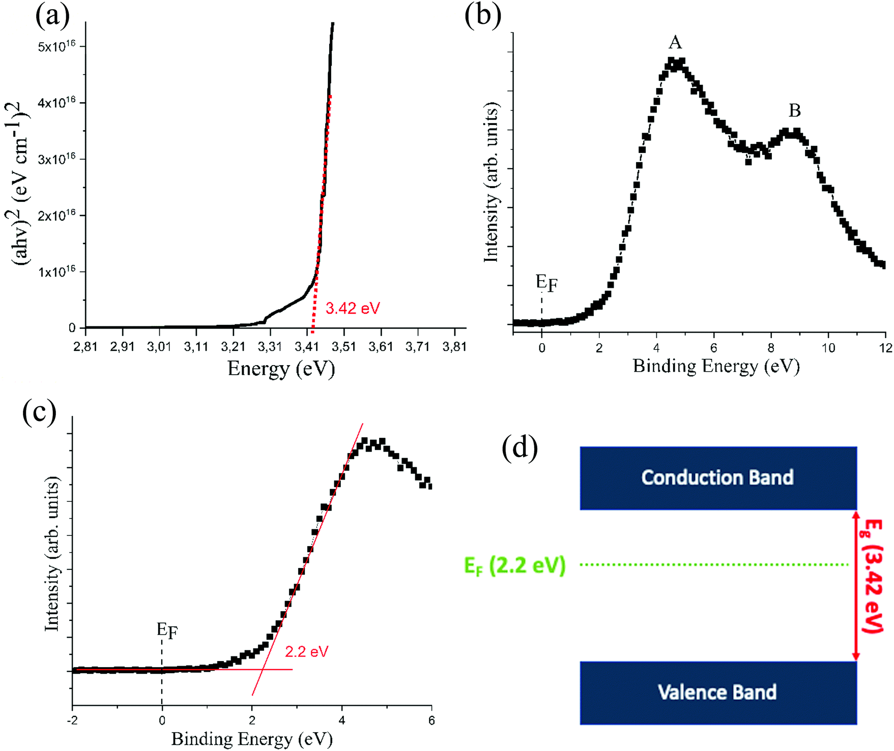 | ||
| Fig. 6 (a) The absorption spectrum for the GaN deposited at 250 °C with a 4 s pulse of 1 and 9 s NH3 plasma pulse on Si (100) with a thickness of approximately 70 nm. (b) The valence band spectrum of the GaN film with a thickness of approximately 70 nm obtained by XPS. (c) The near Fermi level (EF) region together with the valence band maxima obtained from extrapolating the baseline with the linear fit of the XPS spectrum. (d) Schematic illustration of the energy band diagram for GaN deposited at 250 °C. | ||
By replacing the Si (100) substrate with 4H-SiC (0001), which is a more suitable substrate for GaN with respect to the lattice mismatch and crystal structure, XRD in θ–2θ geometry showed only the GaN (0002) and (0004) peaks together with the substrate peaks. This indicates that growth occurred only in the c-direction (Fig. 7a). The GaN film was deposited at 250 °C using a 4 s pulse of 1 and 9 s NH3 plasma pulse. GIXRD of the GaN film grown on SiC showed no peaks, indicating no tilted grains present in the film (Fig. 7b). Pole figures were constructed to investigate the epitaxial relationship between the film and the substrate (Fig. 7c and d). The GaN (10![[1 with combining macron]](https://www.rsc.org/images/entities/char_0031_0304.gif) 3) plane was used due to large difference in the psi angle between GaN and SiC, making it possible to distinguish between the GaN and SiC poles. The pole figure showed six poles, representing the hexagonal GaN lattice with its six-fold symmetry (Fig. 7c). The SiC (102) plane show six poles, representing its hexagonal six-fold symmetry (Fig. 7d). These pole figures show that the hexagonal GaN crystals have grown exactly on top of the SiC crystals, confirming that epitaxial GaN has been grown directly on SiC substrate. The epitaxial relationship between the film and the substrate is GaN (0002)‖SiC (0004) and GaN (103)‖SiC (102). It is worth noting that no AlN interlayer was used to aid the growth of GaN on SiC, which is required for CVD of GaN on SiC.7,43 This opens up the possibility for deposition of GaN on transistor structures without the need of a buffer layer between SiC and GaN.
3) plane was used due to large difference in the psi angle between GaN and SiC, making it possible to distinguish between the GaN and SiC poles. The pole figure showed six poles, representing the hexagonal GaN lattice with its six-fold symmetry (Fig. 7c). The SiC (102) plane show six poles, representing its hexagonal six-fold symmetry (Fig. 7d). These pole figures show that the hexagonal GaN crystals have grown exactly on top of the SiC crystals, confirming that epitaxial GaN has been grown directly on SiC substrate. The epitaxial relationship between the film and the substrate is GaN (0002)‖SiC (0004) and GaN (103)‖SiC (102). It is worth noting that no AlN interlayer was used to aid the growth of GaN on SiC, which is required for CVD of GaN on SiC.7,43 This opens up the possibility for deposition of GaN on transistor structures without the need of a buffer layer between SiC and GaN.
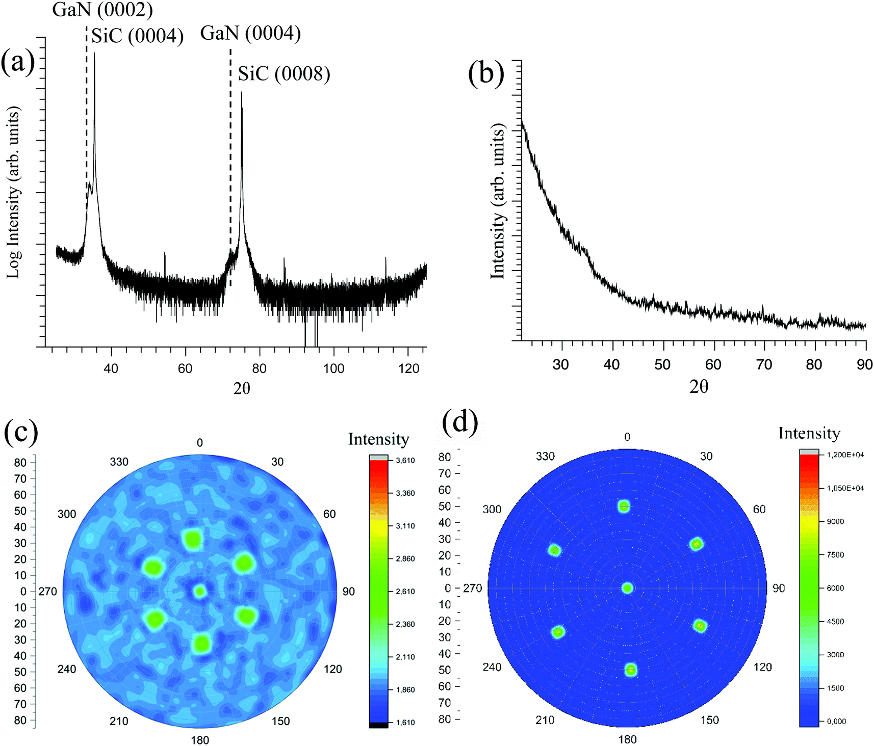 | ||
| Fig. 7 XRD of GaN deposited at 250 °C with 4 s of 1 and 9 s NH3 plasma with a thickness of approximately 70 nm. (a) θ–2θ showing the (0002) and (0004) plane of hexagonal GaN (b) GiXRD showing no present peaks indicating no tilted grains for GaN on SiC. (c) Pole figure of (103) plane for GaN showing six poles of hexagonal GaN. (d) Pole figure of (102) plane for 4H-SiC substrate showing six poles representing its six-fold symmetry. | ||
Top-view SEM of the GaN film on SiC deposited at 250 °C was composed of larger grains compared to GaN on Si substrate (Fig. S3, ESI†).
Further structural characterization was undertaken using scanning transmission electron microscopy (STEM) with high angle annular dark field (HAADF) imaging and SAED). An overview cross-sectional STEM-HAADF image, along [11![[2 with combining macron]](https://www.rsc.org/images/entities/char_0032_0304.gif) 0], together with corresponding SAED patterns (shown in the insets) acquired from the film and substrate are shown in Fig. 8a. According to the STEM-HAADF images recorded under strong elemental contrast (Z-contrast) conditions, two distinct regions in the film were observed. The film appears uniform starting from film/substrate interface for the first ∼6 nm. Afterward, the growing film starts to develop columnar microstructure, leading to a pronounced surface roughening. The darker STEM-HAADF contrast dotted pattern in the columns and columnar boundaries can be attributed to the presents of point defects, e.g. vacancies and impurities, in the film.
0], together with corresponding SAED patterns (shown in the insets) acquired from the film and substrate are shown in Fig. 8a. According to the STEM-HAADF images recorded under strong elemental contrast (Z-contrast) conditions, two distinct regions in the film were observed. The film appears uniform starting from film/substrate interface for the first ∼6 nm. Afterward, the growing film starts to develop columnar microstructure, leading to a pronounced surface roughening. The darker STEM-HAADF contrast dotted pattern in the columns and columnar boundaries can be attributed to the presents of point defects, e.g. vacancies and impurities, in the film.
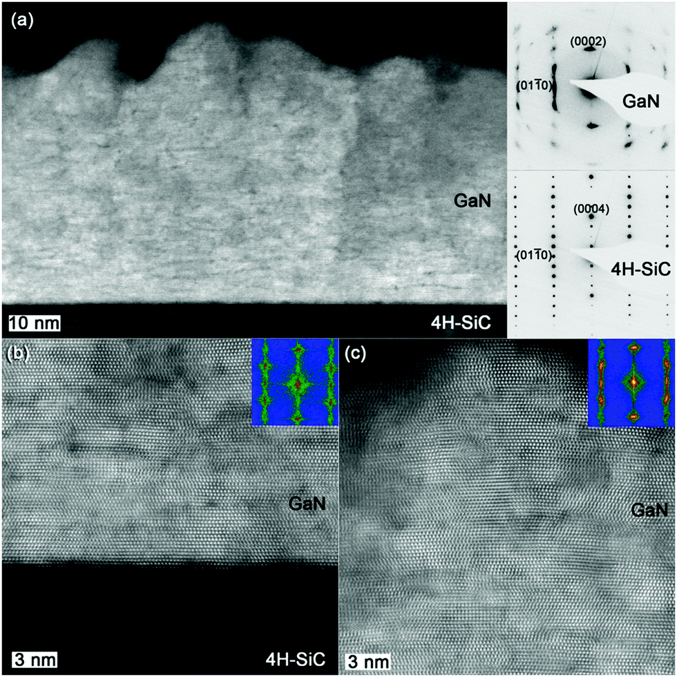 | ||
| Fig. 8 (a) An overview STEM-HAADF image from the GaN film with a thickness of approximately 40 nm on 4H-SiC together with SAED in the insets. HRSTEM-HAADF image from (b) film–substrate interface and (c) the top part of the film. FFT patterns are shown as insets in (b) and (c). | ||
The epitaxial grown GaN film on 4H-SiC can be identified by SAED pattern shown as insets in Fig. 8a. The GaN is oriented with the c-axis perpendicular to the 4H-SiC substrate surface, GaN [0002]‖SiC [0002] and the in-plane relation GaN [010]‖SiC [010]. According to our HRSTEM-HAADF imaging and the Fast Fourier Transforms (FFTs), the stacking of the GaN lattice planes is more ordered close to the GaN–SiC interface compared to the upper part of the film (Fig. 8b). The arc-shaped diffraction spots associated with GaN (inset in Fig. 8a), indicating part of GaN crystal is deviated from the ideal c-axis epitaxy, are ascribed to the curved stacking of (0002) planes for the upper part of the film (Fig. 8c). The lattice curvature together with various types of structural imperfections becomes more and more pronounced for the top part of the film. The GaN film can accommodate the stress in the beginning of the growth, the first ∼6 nm as evidenced from Fig. 8b. We believe that when the GaN grows over this critical thickness the increased stress (due to compressive lattice mismatch of 3% with the substrate) forces the GaN planes to curve. The curvature of the planes increases along the c-direction, further away from film/substrate interface. X-ray Rocking Curve (XRC) was employed on the epitaxial GaN, showing that the full width at half maximum (FWHM) for the (0002) plane was 523 arcsec (0.1452°), Fig. S2 (ESI†). This is on par with previous high temperature CVD study of GaN films were an AlN seed layer was deposited on the SiC substrate.8 These findings could revolutionize the transistor industry, especially for the production of high electron mobility transistors (HEMTs). Being able to deposit very thin GaN directly on SiC without the need for an AlN seed layer allows for increased design freedom when producing HEMTs, which could in turn improve their performance.
Finally, a thermal ALD route to GaN was investigated using 1 and NH3 without plasma discharge. The same pulse parameters were used as the plasma process, but a 16 s of NH3 pulse was used in a temperature range of 150–400 °C. GaN films could also be obtained via this thermal process, however, the films were X-ray (θ–2θ and GIXRD) amorphous. The XPS analysis showed the films contained high amounts of C and O impurities, 4 at% and 15 at%, respectively (Fig. S4, ESI†). The Ga/N ratio could not be accurately be measured due to the Ga Auger overlap with N 1s. The high level of impurities could explain the amorphous nature of these films, which are likely to distort the long-range order of the atoms in the lattice. This also highlights the efficiency of the NH3 plasma to remove carbon and oxygen impurities from the growing film surface.
Conclusions
We successfully deposited GaN on Si (100) and 4H-SiC (0001) using tris(dimethylamido)gallium(III) together with NH3 by both thermal and plasma ALD. The NH3 plasma process showed that surface saturation could be obtained with a GPC of 1.4 Å per cycle after 4 s of 1 and 6 s of NH3 plasma. The growth per cycle was independent of temperature between 130–250 °C and the growth rate was 3–5 times higher than previously reported ALD of GaN. The deposited film at 250 °C showed a Ga/N ratio of 0.97 with 2.8 at% of C and 3 at% of O measured by RBS/ERDA. A Tauc plot revealed that the deposited GaN had an optical bandgap of 3.42 eV. XPS measurements showed that the Fermi level lies closer to the conduction band in comparison to the valence band, indicating unintentionally n-type doped GaN films. Pole figure measurements showed that epitaxial GaN was deposited directly on 4H-SiC (0001), without any buffer layer, with NH3 plasma at 250 °C. The epitaxial relationships were determined as GaN (0002)‖SiC (0004) and GaN (103)‖SiC (102). SAED confirmed the epitaxial relationship between the GaN film and SiC substrate. This is to our knowledge the first epitaxial GaN on SiC without a buffer layer. The STEM-HAADF images also revealed that the GaN planes starts to curve along the growth direction after a critical thickness of approximately 6 nm. XRC shows that the GaN (0002) has a FWHM of 523 arc sec which similar to that of CVD grown GaN. The thermal route rendered X-ray (θ–2θ and GIXRD) amorphous GaN in the temperature range of 150–400 °C. The high impurity levels in the thermal GaN films are believed to be the reason for its amorphous nature.
These findings could open up the doors for new and smaller HEMTs based on group 13 nitrides. By being able to deposit high quality GaN films at these low temperatures also present the opportunity to deposit on temperature sensitive materials which has previously been hindered due to the high deposition temperatures. The ability to deposit GaN directly on SiC also reduces the number of material interfaces which could potentially improve the transistor performance.
Conflicts of interest
There are no conflicts to declare.Acknowledgements
This project was founded by the Swedish foundation for Strategic Research through the project “Time-resolved low temperature CVD for III-nitrides” (SSF-RMA 15-0018) and by the Knut and Alice Wallenberg foundation through the project “Bridging the THz gap” (no. KAW 2013.0049). Support from the Swedish research council VR-RFI (2017-00646_9) for the Accelerator based ion-technological center, and from the Swedish Foundation for Strategic Research (RIF14-0053) for the tandem accelerator laboratory in Uppsala is gratefully acknowledged. The authors acknowledge the Knut and Alice Wallenberg Foundation for supporting the Linköping electron microscopy laboratory and Seán T. Barry for access to TGA and DSC instruments at Carleton University, Canada.References
- S. Strite and H. Morkoç, J. Vac. Sci. Technol., B, 1992, 10, 1237–1266 CrossRef CAS.
- S. Porowski, Mater. Sci. Eng., B, 1997, 44, 407–413 CrossRef.
- E. Lakshmi, Thin Solid Films, 1981, 83, 137–140 CrossRef.
- M. Suzuki, T. Uenoyama and A. Yanase, Phys. Rev. B: Condens. Matter Mater. Phys., 1995, 52, 8132–8139 CrossRef CAS PubMed.
- A. A. Burk, M. J. O’Loughlin, R. R. Siergiej, A. K. Agarwal, S. Sriram, R. C. Clarke, M. F. MacMillan, V. Balakrishna and C. D. Brandt, Solid-State Electron., 1999, 43, 1459–1464 CrossRef CAS.
- GaN-Based Materials and Devices, ed. M. S. Shur and R. F. Davis, World Scientific Publishing Co. Pte. Ltd., Singapore, 2004 Search PubMed.
- K. Tamura, Y. Kuroki, K. Yasui, M. Suemitsu, T. Ito, T. Endou, H. Nakazawa, Y. Narita, M. Takata and T. Akahane, Thin Solid Films, 2008, 516, 659–662 CrossRef CAS.
- J. Lu, J. T. Chen, M. Dahlqvist, R. Kabouche, F. Medjdoub, J. Rosen, O. Kordina and L. Hultman, Appl. Phys. Lett., 2019, 115, 221601 CrossRef.
- J.-T. Chen, J. Bergsten, J. Lu, E. Janzén, M. Thorsell, L. Hultman, N. Rorsman and O. Kordina, Appl. Phys. Lett., 2018, 113, 041605 CrossRef.
- B. L. Liu, M. Lachab, A. Jia, A. Yoshikawaa and K. Takahashi, J. Cryst. Growth, 2002, 234, 637–645 CrossRef CAS.
- C. Ozgit-Akgun, E. Goldenberg, A. K. Okyay and N. Biyikil, J. Mater. Chem. C, 2014, 2, 2123–2136 RSC.
- C. Ozgit, I. Donmez, M. Alevli and N. Biyikli, J. Vac. Sci. Technol., A, 2012, 30, 01A124 CrossRef.
- S. Banerjee, A. A. I. Aarnink, D. J. Gravesteijn and A. Y. Kovalgin, J. Phys. Chem. C, 2019, 123, 23214–23225 CrossRef CAS.
- M. Alevli, A. Haider, S. Kizir, S. A. Leghari and N. Biyikli, J. Vac. Sci. Technol., A, 2016, 34, 01A137 CrossRef.
- P. Motamedi, N. Dalili and K. Cadien, J. Mater. Chem. C, 2015, 3, 7428–7436 RSC.
- Y. Kumagai, M. Mayumi, A. Koukitu and H. Seki, Appl. Surf. Sci., 2000, 159, 427–431 CrossRef.
- O. H. Kim, D. Kim and T. Anderson, J. Vac. Sci. Technol., A, 2009, 27, 923–928 CrossRef CAS.
- R. G. Gordon, in Atomic Layer Deposition for Semiconductors, ed. C. S. Hwang and C. Y. Yoo, Springer, US, New York, 2014, pp. 15–46 Search PubMed.
- R. O’Donoghue, J. Rechmann, M. Aghaee, D. Rogalla, H. W. Becker, M. Creatore, A. D. Wieck and A. Devi, Dalton Trans., 2017, 46, 16551–16561 RSC.
- C. L. Dezelah IV, J. Niinistö, K. Arstila, L. Niinistö and C. H. Winter, Chem. Mater., 2006, 18, 471–475 CrossRef.
- X. Meng, J. A. Libera, T. T. Fister, H. Zhou, J. K. Hedlund, P. Fenter and J. W. Elam, Chem. Mater., 2014, 26, 1029–1039 CrossRef CAS.
- D. M. Hoffman, S. Prakash Rangarajan, S. D. Athavale, D. J. Economou, J. Liu, Z. Zheng and W. Chu, J. Vac. Sci. Technol., A, 1996, 14, 306–311 CrossRef CAS.
- K. M. Waggoner, M. M. Olmstead and P. P. Power, Polyhedron, 1990, 9, 257–263 CrossRef CAS.
- W. Kern and A. D. Puotinen, RCA Rev., 1970, 31, 187–206 CAS.
- P. Deminskyi, P. Rouf, I. G. Ivanov and H. Pedersen, J. Vac. Sci. Technol., A, 2019, 37, 020926 CrossRef.
- M. Mayer, W. Eckstein, H. Langhuth, F. Schiettekatte and U. Von Toussaint, Nucl. Instrum. Methods Phys. Res., Sect. B, 2011, 269, 3006–3013 CrossRef CAS.
- P. Ström, P. Petersson, M. Rubel and G. Possnert, Rev. Sci. Instrum., 2016, 87, 103303 CrossRef PubMed.
- K. S. Janson, CONTES, Uppsala University, 2004 Search PubMed.
- K. Arstila, J. Julin, M. I. Laitinen, J. Aalto, T. Konu, S. Kärkkäinen, S. Rahkonen, M. Raunio, J. Itkonen, J. P. Santanen, T. Tuovinen and T. Sajavaara, Nucl. Instrum. Methods Phys. Res., Sect. B, 2014, 331, 34–41 CrossRef CAS.
- Y. Zhang, H. J. Whitlow, T. Winzell, I. F. Bubb, T. Sajavaara, K. Arstila and J. Keinonen, Nucl. Instrum. Methods Phys. Res., Sect. B, 1999, 149, 477–489 CrossRef CAS.
- M. A. Arvizu, R. T. Wen, D. Primetzhofer, J. E. Klemberg-Sapieha, L. Martinu, G. A. Niklasson and C. G. Granqvist, ACS Appl. Mater. Interfaces, 2015, 7, 26387–26390 CrossRef CAS PubMed.
- H. Y. Qu, D. Primetzhofer, M. A. Arvizu, Z. Qiu, U. Cindemir, C. G. Granqvist and G. A. Niklasson, ACS Appl. Mater. Interfaces, 2017, 9, 42420–42424 CrossRef CAS PubMed.
- J. F. Ziegler, M. D. Ziegler and J. P. Biersack, Nucl. Instrum. Methods Phys. Res., Sect. B, 2010, 268, 1818–1823 CrossRef CAS.
- M. Fujikane, M. Leszczyński, S. Nagao, T. Nakayama, S. Yamanaka, K. Niihara and R. Nowak, J. Alloys Compd., 2008, 450, 405–411 CrossRef CAS.
- G. Moldovan, M. J. Roe, I. Harrison, M. Kappers, C. J. Humphreys and P. D. Brown, Philos. Mag., 2006, 86, 2315–2327 CrossRef CAS.
- Z. Majlinger, A. Bozanic, M. Petravic, K. J. Kim, B. Kim and Y. W. Yang, Vacuum, 2009, 84, 41–44 CrossRef CAS.
- M. Kumar, A. Kumar, S. B. Thapa, S. Christiansen and R. Singh, Mater. Sci. Eng., B, 2014, 186, 89–93 CrossRef CAS.
- S. S. Kushvaha, M. S. Kumar, M. Maheshwari, A. K. Shukla, P. Pal and K. K. Maurya, Mater. Res. Express, 2014, 1, 035903 CrossRef.
- D. Skuridina, D. V. Dinh, B. Lacroix, P. Ruterana, M. Hoffmann, Z. Sitar, M. Pristovsek, M. Kneissl and P. Vogt, J. Appl. Phys., 2013, 114, 1735 CrossRef.
- X. Xu, H. Liu, C. Shi, Y. Zhao, S. Fung and C. D. Beling, J. Appl. Phys., 2001, 90, 6130–6134 CrossRef CAS.
- J. Neugebauer and C. G. Van De Walle, Appl. Phys. Lett., 1996, 69, 503–505 CrossRef.
- J. Neugebauer and C. G. Van De Walle, Phys. Rev. B: Condens. Matter Mater. Phys., 1994, 50, 8067–8070 CrossRef CAS PubMed.
- N. V. Edwards, M. D. Bremser, R. F. Davis, A. D. Batchelor, S. D. Yoo, C. F. Karan and D. E. Aspnes, Appl. Phys. Lett., 1998, 73, 2808–2810 CrossRef CAS.
Footnote |
| † Electronic supplementary information (ESI) available. See DOI: 10.1039/d0tc02085k |
| This journal is © The Royal Society of Chemistry 2020 |