
 Open Access Article
 This Open Access Article is licensed under a Creative Commons Attribution-Non Commercial 3.0 Unported Licence
Doping of silicon by phosphorus end-terminated polymers: drive-in and activation of dopants
Michele
Perego
 *a,
Francesco
Caruso
ab,
Gabriele
Seguini
a,
Elisa
Arduca
a,
Roberto
Mantovan
a,
Katia
Sparnacci
c and
Michele
Laus
c
*a,
Francesco
Caruso
ab,
Gabriele
Seguini
a,
Elisa
Arduca
a,
Roberto
Mantovan
a,
Katia
Sparnacci
c and
Michele
Laus
c
aCNR-IMM, Unit of Agrate Brianza, Via C. Olivetti 2, I-20864 Agrate Brianza, Italy. E-mail: michele.perego@cnr.it
bUniversità degli Studi di Milano, Via Celoria 16, I-20133 Milano, Italy
cUniversità del Piemonte Orientale “A. Avogadro”, Viale T. Michel 11, I-15121 Alessandria, Italy
First published on 19th May 2020
Abstract
An effective doping technology for the precise control of P atom injection and activation into a semiconductor substrate is presented. Polystyrene polymers with a narrow molecular weight distribution and end-terminated with a P containing moiety are used to build up a phosphorus δ-layer to be used as the dopant source. P atoms are efficiently injected into the Si substrate by high temperature (900–1250 °C) thermal treatments. Temperature dependent (100–300 K) resistivity and Hall measurements in the van der Pauw configuration demonstrate high activation rates (ηa > 80%) of injected P atoms. This bottom-up approach holds promise for the development of a mild technology for efficient doping of semiconductors.
Introduction
Semiconductor technology relies on the capability for tuning the electrical properties of the substrate through the controlled introduction of substitutional impurities (doping) in the crystal lattice of the semiconductor host material, in order to tailor its electronic, optical and/or magnetic properties.1 However, the present ex situ doping strategies cannot be easily extended to the nanoscale. As the size of semiconductor devices shrinks to the nanoscale, the standard random distribution of the individual atoms within the semiconductor becomes critical since the assumption of uniform doping distribution does not hold anymore.2,3 Currently there is a significant effort by the scientific community for the development of a new technology to demonstrate deterministic doping of semiconductor structures at the nanoscale.Conventional doping techniques are mainly based on ion implantation which implies the bombardment of the target semiconductor with high energy dopant-containing ions that, subsequently, are induced to replace atoms in the lattice using a high temperature thermal treatment.1 The main advantage of this technique is the independent control of the dopant dose and depth distribution of the impurity atoms within the semiconductor host. This approach has been widely explored, and has become the workhorse in microelectronics, since it guarantees excellent doping uniformity over large areas. Nevertheless, there are a number of drawbacks that are associated with ion implantation technology, including damage to the crystal lattice during ion bombardment and subsequent transient enhanced diffusion caused by defects during the thermal treatment.4 Moreover, most of the source gases, commonly used in ion implantation, are hazardous from a health and environmental perspective.5 Finally, this technique is incompatible with 3D nanostructured materials since it does not provide conformal dopant incorporation for non-planar nanostructures.6
Plasma immersion ion implantation, also referred to as plasma doping, is an emerging technique based on the extraction of accelerated ions from a plasma by applying a high voltage in order to implant them in a semiconductor substrate.7 This technique offers significant advantages over conventional ion implantation, since the doping profiles are generally more conformal than those obtained using conventional ion implantation. However, even in this case, there are several problems due to crystal damage and, at the same time, difficulties in doping with multiple species at different energies in a single process.5 Moreover, all these ion-based approaches present significant drawbacks when applied to compound semiconductors composed of two or more chemically and electronically non-equivalent lattice sites, since the stoichiometry of the target matrix can be locally modified from implantation induced crystal damage.1
Alternative approaches based on gas phase or solid phase diffusion have been investigated as well, but they face fundamental limits in controlling dopant concentration near the surface and a lack of uniformity.1 Spin-on doping technology consists of the deposition of a dopant-containing solution onto the semiconductor surface, followed by a diffusion-annealing step. The dopant-containing solution is usually formed by either a mixture of SiO2 and dopant atoms or Si-containing polymers with dopant atoms incorporated into the polymeric chains, like phosphosilicates or borosilicates.8 Unfortunately, this simple and nondestructive technique does not guarantee accurate dose control over large areas of the substrate. In addition, residues left over from the solution containing the dopant precursor are not easily removed from the surface, resulting in a chemically modified layer that is very difficult to be stripped off.5 Self-assembly strategies followed by molecule grafting have been demonstrated to be effective in generating a uniform monolayer of dopant-containing molecules tethered to the pristine crystalline Si substrates over large areas.9 Assuming a sufficiently high number of reactive sites on the substrates, the effective density of grafted molecules is ultimately determined by the molecule footprint. This self-limiting reaction has been used in combination with conventional spike annealing to enable the formation of B, P and As sub-5 nm ultra-shallow junctions in Si.6,9–11 Nanoscale doping of InAs,12,13 InxGAyAsz,14,15 InP,16 Ge17–19 and SiGe20via monolayers of dopant containing molecules has been demonstrated as well. This gentle approach, usually referred to as monolayer doping (MLD), has been proven to be efficient in introducing controlled amounts of dopants in Si nanowires9 and InP nanopillars.16 MLD is very versatile as, in principle, surface preparation, molecular footprint, capping layer and thermal treatment parameters can be finely tuned to optimize surface coverage of the molecules and diffusion of the dopant into the semiconductor. However, the wet chemistry commonly used in the MLD process significantly limits the manufacturability of this process technology.9 Moreover, dopant concentrations obtained by MLD are ∼1020 cm−3. The extension of this approach to doping concentrations in the range of 1015–1021 cm−3 is essential for its industrial exploitation. A modified MLD approach was proposed as a strategy to reproducibly control the doping dose.21 The dopant-containing molecules are mixed with dopant free molecules and subsequently grafted onto the Si surface. The final monolayer composition is assumed to be proportional to the fraction of dopant-containing molecules in the solution. In this way, the doping dose was varied over 1 order of magnitude, but reproducibility and accuracy of this approach are questionable.21 Finally carbon and oxygen contamination can be introduced into the silicon substrate during the drive-in process, forming complex defects that affect the electrical properties of the semiconductor substrate. Interstitial carbon can form pairs with group-V dopants, like phosphorus, arsenic and antimony, creating multiple deep energy levels into the gap of the semiconductor.22 Carbon related defects have been reported to significantly decrease the P activation rate,23 suggesting that new processes are necessary to remove the carbon of the dopant carrying molecules before the high temperature drive-in thermal treatment.
Recently, we synthesized narrow molar mass distribution polymers terminated with P-containing moieties. These dopant-carrying polymers were thermally grafted to the not-deglazed and deglazed silicon substrates from the melt.24–26 Due to the self-limiting nature of the “grafting-to” reaction, these molecules form a brush layer, whose thickness depends on the molar mass of the utilized dopant polymer, irrespective of the oxidation of the Si surface. Efficient tuning of the areal density of the grafted molecules over the target substrate and consequently the final number of P atoms in the dopant source was demonstrated. Polymeric chains were removed by plasma treatment before the deposition of the SiO2 capping layer, acting as a diffusion barrier during the drive-in process. Subsequent injection and activation of P atoms into the Si substrate, with negligible carbon and oxygen contaminations, was achieved by high temperature annealing.24 Repeated cycles of grafting and O2 plasma removal of the polymeric chains were demonstrated to progressively increase the P dose in the dopant source.24 In this work, we investigate the efficiency of this doping approach as a function of P areal dose and drive-in processing conditions, to assess the potential of this technology as a feasible solution for the development of a gentle doping platform for next generation microelectronics devices.
Experimental
Materials
A hydroxy-terminated polystyrene (PS) homopolymer was synthesized by ARGET-ATRP copolymerization of styrene. The sample was subsequently reacted with diethylchlorophosphate (DPP). The resulting P-terminated polymer (PS-P) presents average molar mass Mn = 2.3 ± 0.3 kg mol−1, polydispersity index Đ = 1.05 ± 0.01, and degree of polymerization N = 17 ± 3. More information about the synthesis and characterization of the P-terminated polymer is available in previous publications.24,25 The substrates were prepared from nearly intrinsic (ρ > 5 kΩ cm) floating zone (FZ) single-side polished Si (100) wafers purchased from Siltronix.Substrate cleaning
Wafers were cleaved into 0.9 × 0.9 cm2 pieces and treated with Piranha solution (H2SO4 and H2O2 in a 3![[thin space (1/6-em)]](https://www.rsc.org/images/entities/char_2009.gif) :1 ratio) at 80 °C for 40 min, followed by rinsing with deionized water for 5 min. Piranha solution was used to clean the sample surface from all organic impurities and to promote grafting by increasing the surface density of hydroxyl groups. Finally, the samples were dried under N2 flow, and the native SiO2 layer thickness was measured by ellipsometry.
:1 ratio) at 80 °C for 40 min, followed by rinsing with deionized water for 5 min. Piranha solution was used to clean the sample surface from all organic impurities and to promote grafting by increasing the surface density of hydroxyl groups. Finally, the samples were dried under N2 flow, and the native SiO2 layer thickness was measured by ellipsometry.
Sample preparation
The P terminated PS homopolymer was dissolved in toluene (9 mg of homopolymer in 1 ml of toluene) by means of an ultrasonic bath for 5 min. Then the solution was spin coated (30 s at 3000 rpm) on the cleaned substrates to form a uniform polymer film. In order to check the thickness uniformity among the different samples, the polymer layer thickness of each sample was measured by ellipsometry. The average thickness of the spin-coated polymer films was determined to be 27.2 ± 0.9 nm. The samples were then annealed using a rapid thermal processing (RTP) apparatus for 15 min at 190 °C in a N2 atmosphere in order to promote the grafting reaction, following the procedure described elsewhere.24 Temperature was selected in order to avoid any thermal degradation of the P terminated polymers during the grafting process.25,27 During this process, the P containing moiety at the polymer chain end reacts with a hydroxyl group at the SiO2 surface, ultimately forming a uniform brush layer over the native SiO2 layer. Non-grafted chains were washed out by an ultra-sonic bath in toluene for 5 min. Finally, the samples were dried under a N2 flow. The thickness of the final grafted polymeric layer was measured by ellipsometry. The average thickness of the polymeric films over the entire set of samples was 2.43 ± 0.08 nm, that is about two times the radius of gyration of the polymer, in agreement with previous reports in the literature.28 Upon grafting, polymeric chains were removed by O2 plasma ashing (40 W for 5 min) leaving only phosphate groups at the silicon surface. The thickness of the residual polymeric layer after O2 plasma ashing was monitored to confirm complete removal of the PS chains. The phosphorus concentration on the substrate can be increased by repeated cycles of grafting–ashing. Samples with a number of grafting–ashing cycles ranging from 1 to 5 were prepared to obtain dopant sources with different concentrations of P impurity atoms. Once the grafting–ashing procedure was completed, the samples were capped with a 10 nm thick SiO2 layer deposited by e-beam evaporation, forming a P δ-layer source embedded in a SiO2 matrix. P atoms were diffused through the native SiO2 barrier into the Si substrate by high temperature thermal treatment performed in a RTP system. In more detail, samples were annealed in an N2 atmosphere at temperatures ranging from 1000 to 1250 °C for 5 s with a ramp temperature of 50 °C s−1. Upon removal of SiO2 capping layers by HF dipping and subsequent washing in deionized H2O, aluminum metal contacts were deposited by thermal evaporation using a shadow mask. The metal contacts are circular dots with diameter ∼1.2 mm placed at the sample corners. A picture of a typical sample with the Al metal contacts is shown in the inset of Fig. 1a.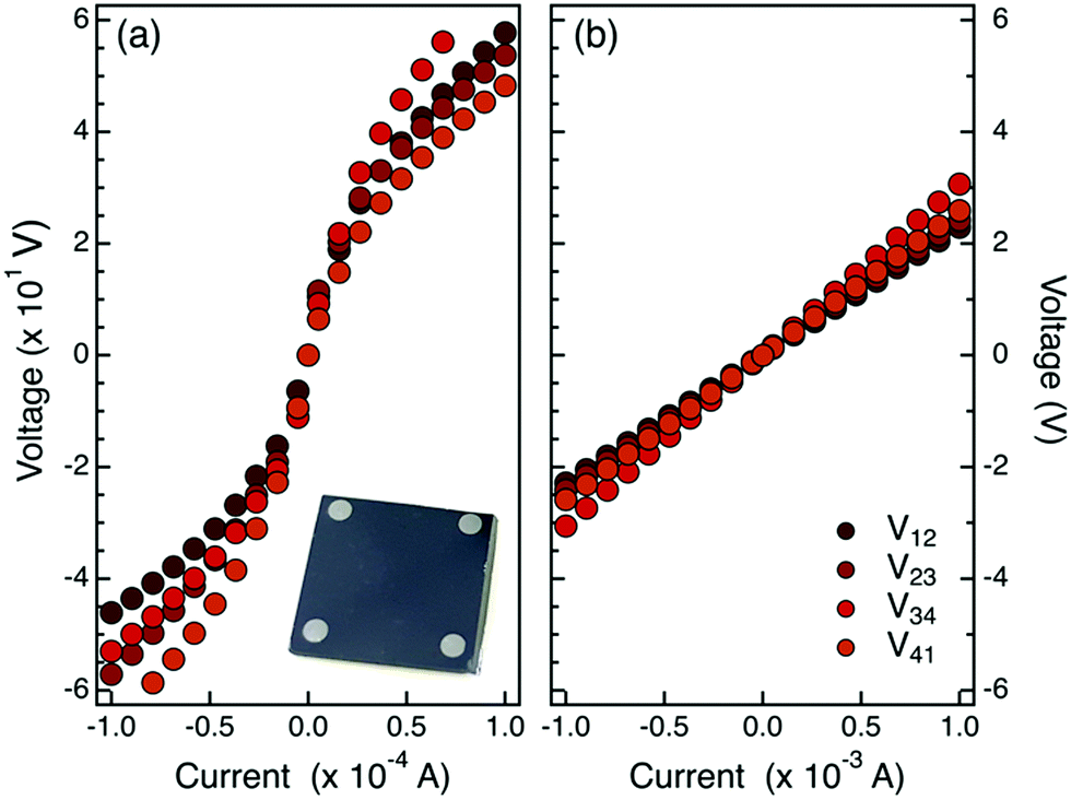 | ||
| Fig. 1 I–V characteristics of the different pairs of contacts for the samples obtained with 1 cycle of grafting–O2 plasma ashing followed by high temperature annealing in RTP at T = 1000 °C (a) and T = 1250 °C (b) respectively. For each sample, different I–V curves were acquired, measuring the tension Vij between two adjacent contacts when a current Iij is applied and considering all the possible combinations of adjacent metal contacts i = {1,…,4} and j = i + 1. A picture of a typical 0.9 × 0.9 cm2 Si sample with Al metal contacts deposited at each corner is depicted in the inset. | ||
Phosphorous quantification.
Time of Flight Secondary Ion Mass Spectrometry (ToF-SIMS) depth profiles were performed using a dual beam IONTOF IV system operating in negative mode. Cs+ ions (@ 1 keV and 80 nA) and Ga+ ions (@ 25 keV and 1 pA) were used for sputtering and analysis, respectively. 16 nm-thick silicon on the insulator reference sample was used to measure sputter velocity and calibrate the depth scale. P concentration profiles were obtained by accurate calibration of the P signals in the Si matrix by means of an analytical protocol that is described in previous publications.29,30Electrical characterization
Sheet resistance and Hall measurements were obtained in the van der Pauw geometry using a closed-cycle cryostat, at temperatures ranging between 100 K and 300 K. A constant current (I) is applied through the Keithley 6221 while the Keithley 2182A nanovoltmeter records the corresponding voltages (V). Current/voltages can be injected/measured in a custom mode across the four aluminum metal contacts, thus allowing us to record two-point I–V curves. For Hall measurements, a magnetic field of up to 0.8 T is applied. The data are recorded with a custom-written Labview-based acquisition software.Results and discussion
The injection and activation of P impurity atoms were investigated as a function of the temperature T of the drive-in process. P dopant sources were prepared by a single cycle of grafting and O2 plasma cleaning over a not-deglazed Si substrate using a P terminated polystyrene (PS) sample (Mn = 2.3 ± 0.3 kg mol−1, Đ = 1.05 ± 0.01). To explore the effect of annealing temperature, P injection and activation in the high resistivity (100) Si substrates were performed by RTP treatments at temperatures ranging from 1000 °C to 1250 °C for 5 s.Preliminary analysis of the metal contacts was performed by measuring the I–V characteristic at room temperature for each pair of contacts of this set of samples. The representative I–V curves obtained from the samples annealed at 1000 °C and 1250 °C are reported in Fig. 1a and b, respectively. Collected data indicate that samples annealed at T ≤ 1100 °C present a non-linear current voltage characteristic indicating a non-Ohmic behavior of the contacts. Conversely, samples annealed at T ≥ 1150 °C exhibit a perfectly linear behavior indicating that good Ohmic contacts were formed. It is worth remembering that for contacts with a high doping concentration, the barrier width becomes very narrow, and the tunneling current becomes dominant. Accordingly, experimental data suggest that different amounts of P atoms have been introduced into the Si substrate depending on the annealing temperature of the drive-in process. In particular, at high annealing temperatures the P concentration at the metal–semiconductor interface is so high that tunneling is possible across the potential barrier between the metal and the semiconductor, resulting in a Ohmic behavior of the I–V characteristics.1
The sheet resistance (Rs), carrier concentration (σ), and carrier mobility (μ) values for the set of samples annealed in the 1000–1250 °C range are depicted in Fig. 2. All measurements are recorded in the van der Pauw geometry through the four aluminum contacts at the corners. In particular, the current (Iij) is injected between two adjacent i and j = i + 1 contacts, and the voltage drop (Vkl) is measured across the opposite k = i + 2 and l = k + 1 contacts. A schematic picture of the probe configuration is sketched in the inset of Fig. 2a. From the measured (Iij, Vkl) values, we determined the sheet resistance Rs of the samples. Fig. 2a shows the evolution of Rs as a function of the annealing temperature in a 5 s long RTP process for P dopant injection/activation. The black dashed lines indicate the Rs values measured in the high resistivity pristine substrate and in the same sample after annealing at 1250 °C for 5 s. The Rs reduction upon high temperature annealing in the high resistivity substrate is associated with the formation of oxygen-related thermal donors.31,32 The values are reported as a reference to demonstrate the effective modification of the sheet resistance due to the injection and activation of the P impurities into the Si substrate. Collected data indicate a progressive decrease of the sheet resistance Rs as a function of the annealing temperature, in perfect agreement with data reported in our previous work.24
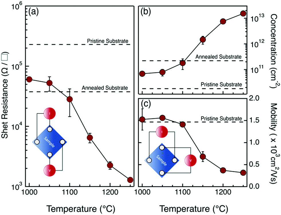 | ||
| Fig. 2 (a) Sheet resistance (Rs) values as function of the annealing temperature (T) during the drive-in process. Rs values of the pristine and annealed (T = 1250 °C) substrate are indicated by black dashed lines. The inset indicates the configuration of the probes on the contacts during van der Pauw measurements. (b) Dopant concentration (σ) and (c) carrier mobility (μ) values as a function of the annealing temperature (T) during the drive-in process. The corresponding σ and μ values of the pristine substrate are indicated by black dashed lines. The σ value of the annealed (T = 1250 °C) substrate is indicated by a black dashed line. The inset indicates the configuration of the probes on the contacts during Hall effect measurements. Each data point was obtained by repeated measurements performed on two different samples prepared with the same number of grafting–ashing cycles and drive-in treatment. | ||
Hall effects measurements were performed using a van der Pauw configuration with the probes placed at the four corners of the sample, following the arrangement shown in Fig. 2c. Current (Iik) was injected between two contacts i and k = i + 2 at the opposite corners of the sample and the voltage drop (Vjl) was measured across the other two contacts j = i + 1 and l = k + 1. The carrier concentration σ and the carrier mobility μ were obtained from the analysis of the collected data using a constant doping approximation.9Fig. 2b and c depict the evolution of σ and μ as a function of the annealing temperature T of the drive-in process. The corresponding σ and μ values of the pristine high resistivity substrate are indicated by the black dashed lines. The σ value of the annealed (1250 °C, 5 s) substrate is indicated in Fig. 2b by the black dashed line. The increase of carrier concentration upon annealing in the undoped high resistivity substrate is associated with the formation of thermal donors. The concentration of thermal donors upon annealing is determined to be ∼2 × 1011 cm−3, in perfect agreement with literature data.32 Increasing the annealing temperature, we observed a progressive increase in the carrier concentration and a concomitant reduction of carrier mobility, in accordance with literature data.1,9 It is interesting to note that, at annealing temperatures T ≤ 1100 °C, the σ values exhibit a limited variation with respect to pristine substrate and the corresponding μ values are perfectly consistent with n-type carrier mobility in intrinsic or low doped silicon.1 Conversely, at T ≥ 1150 °C, data indicate a significant enhancement of the concentration of mobile charges σ, that corresponds to a substantial drop of the carrier mobility μ. The measured μ values suggest that, in samples annealed at T ≥ 1150 °C, dopant concentrations in the surface layer of the sample are expected to be ρ ≥ 1 × 1018 cm−3.1 These results are perfectly consistent with the observed formation of good Ohmic contacts for samples annealed at T ≥ 1150 °C. The high temperature required to promote effective P diffusion and activation in the Si substrate is essentially associated with the presence of a 1.5 nm thick native SiO2 film on the surface of the not-deglazed silicon substrate. In fact, P diffusion in SiO2 is very slow even at relatively high temperatures.33–36 Accordingly, the native SiO2 film represents a diffusion barrier that prevents efficient P injection into the Si substrate unless very high temperatures (T ≥ 1100 °C) are applied.33 In this respect, it is interesting to focus on the high temperature processes, in order to generate high dopant concentration in the region close to the surface layer of the silicon substrate.
To investigate the possibility of effectively modulating the dose of P atoms injected into the Si substrate, a second set of samples was prepared with repeated cycles of grafting and O2 plasma ashing over a not-deglazed Si substrate using the same P-terminated PS molecules. The number of grafting–ashing cycles was varied from 1 to 5 in order to progressively increase the P concentration in the dopant sources. The drive-in process was performed in RTP using the same processing conditions (T = 1200 °C, t = 5 s) for all the samples. ToF-SIMS analysis was carried out to characterize the doping profile of the thermally diffused P atoms in silicon. Calibration of the P signals in the Si matrix was performed applying previously developed protocols.29Fig. 3a shows the calibrated ToF-SIMS depth profiles of P in the Si substrate upon drive-in, for the samples with dopant sources obtained with a different number of grafting–ashing cycles. Due to the presence of a native oxide and to well-known artifacts characterizing the initial stages of SIMS analysis,37 the effective quantification of P concentration in the depth profile is not reliable in the so-called transient region, i.e. in the region close to the surface of the sample. From a general point of view, all the samples exhibit a high surface concentration that sharply decreases to 1018 atoms per cm3 within the initial 80 nm of the Si substrate. The maximum surface concentration ranges from 0.7 × 10¹⁹ to 2.5 × 10¹⁹ atoms per cm3, depending on the concentration of P in the dopant source, i.e. on the number of grafting–ashing cycles. It is worth noting that, in principle, the P concentration could be further enhanced by increasing the number of grafting–ashing cycles. ToF-SIMS data were fitted using Gaussian curves (continuous lines in Fig. 3a) neglecting the data points in the initial 5 nm from the sample surface to account for artifacts in the ToF-SIMS depth profile. The Gaussian functions are characterized by a constant standard deviation (σ = 30.3 ± 2.4 nm) consistent with a source limited model for P diffusion in silicon.1 The total dose of P atoms injected into the silicon substrate was obtained by integration of the calibrated P concentration profiles. Fig. 3b reports the P total dose as a function of the number of grafting–ashing cycles. A linear increase in the P dose is observed in agreement with the idea that the dose of P atoms in the dopant source grows stepwise with each cycle.
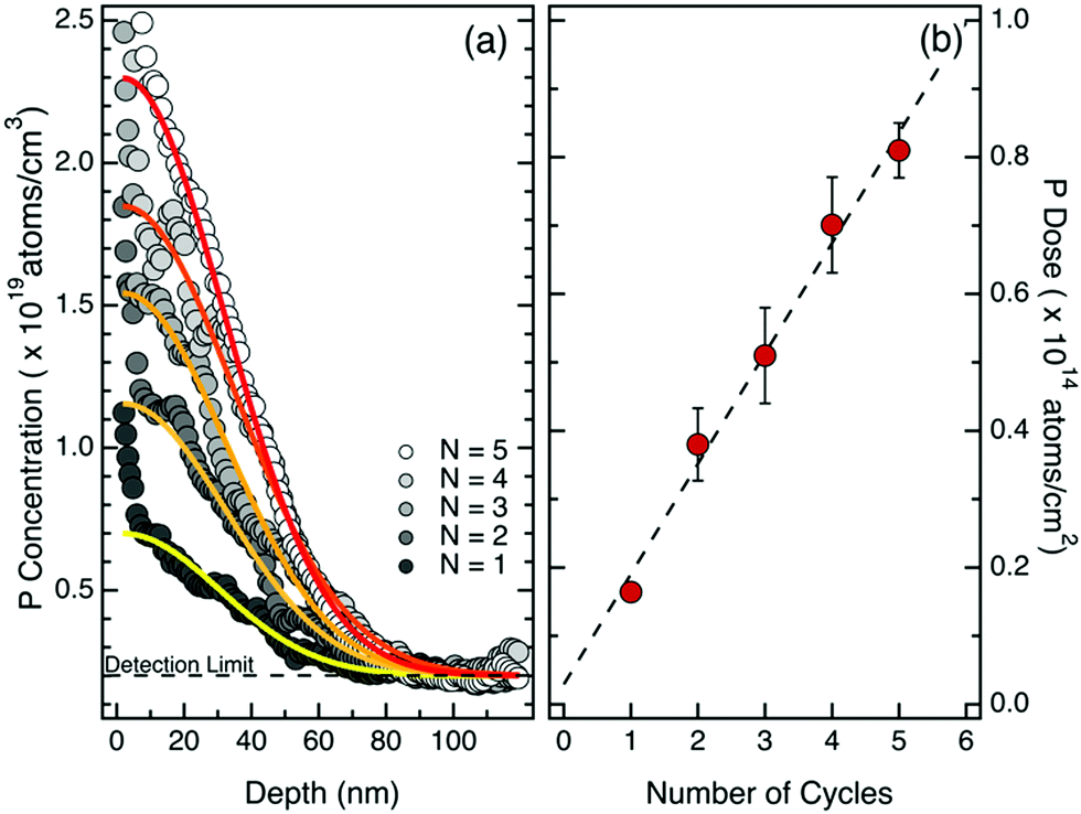 | ||
| Fig. 3 (a) ToF-SIMS calibrated depth profiles showing P distribution in the silicon substrate upon annealing at 1200 °C for 5 s. The P concentration in the dopant source was progressively increased by cycles of grafting-O2 plasma ashing on a not-deglazed Si(100) substrate using a P terminated PS polymer. Grafting was performed at 190 °C in a N2 atmosphere. A 10 nm-thick SiO2 capping layer was deposited on the sample to prevent P out-diffusion during the drive-in process and subsequently removed prior to ToF-SIMS characterization. P calibrated profiles were fitted (continuous lines) assuming a limited source model. The black dashed line indicates the P detection limit of the ToF-SIMS apparatus. (b) Total P dose as function of the number of grafting–O2 plasma ashing cycles. The total number of P atoms in each sample was determined by integration of the P distribution obtained from the calibrated ToF-SIMS profiles. Each data point was obtained by repeated measurements performed on two different samples prepared with the same number of grafting–ashing cycles and drive-in treatment. | ||
Van der Pauw analysis and Hall effect measurements were performed on these samples to obtain information about the electrical activation of the injected P impurity atoms. Fig. 4 reports the values of sheet resistance Rs (a), carrier concentration σ (b) and electron mobility μ (c) as a function of the number of grafting–ashing cycles. Data highlight the progressive Rs reduction determined by the increase in σ that is associated with the higher concentration of P impurity atoms introduced into the Si substrate during the drive-in process. Once again, the gradual decrease of electron mobility μ perfectly correlates with the expected carrier mobility reduction in the case of high dopant concentrations.1 Data suggest that the effective concentration of active dopants in the Si substrate can be accurately modulated by changing the amount of P atoms in the dopant source.
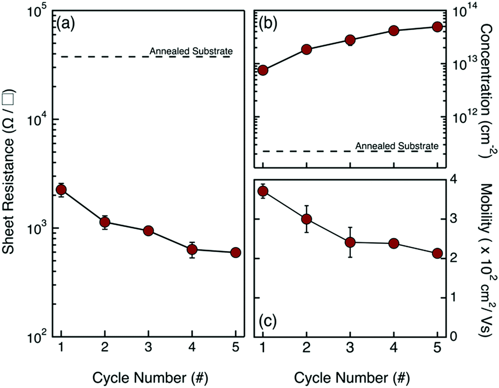 | ||
| Fig. 4 (a) Sheet resistance Rs, (b) carrier concentration σ and (c) carrier mobility μ as a function of the number of grafting–O2 plasma ashing cycles. Each data point was obtained by repeated measurements performed on two different samples prepared with the same number of grafting–ashing cycles. Rs and σ values of the annealed substrate are indicated by black dashed lines. | ||
Fig. 5 reports the free electron concentrations obtained by room temperature Hall effect measurements in a uniform layer approximation versus the ToF-SIMS dose of P atoms for the samples obtained by multiple grafting–ashing cycles. Data exhibit a good linear trend, further confirming that the electrical properties of the Si substrate can be finely tuned by varying the phosphorus concentration in the dopant source. From the slope of the linear fit we obtain the ratio between the free electrons and the phosphorus atoms that corresponds to 66.7%. Gao et al. reported a ratio between the free electron and the phosphorus atoms of 66.6% in a silicon sample doped by MLD, using P containing low molar mass molecules that are quite different from those used in the present work.23 Conversely Wu et al. obtained a value of 26.7% using another P containing molecule.38 This low ratio was explained by observing that electrons ionized from the P dopants were mostly trapped by deep level defects, that are likely carbon interstitials.23
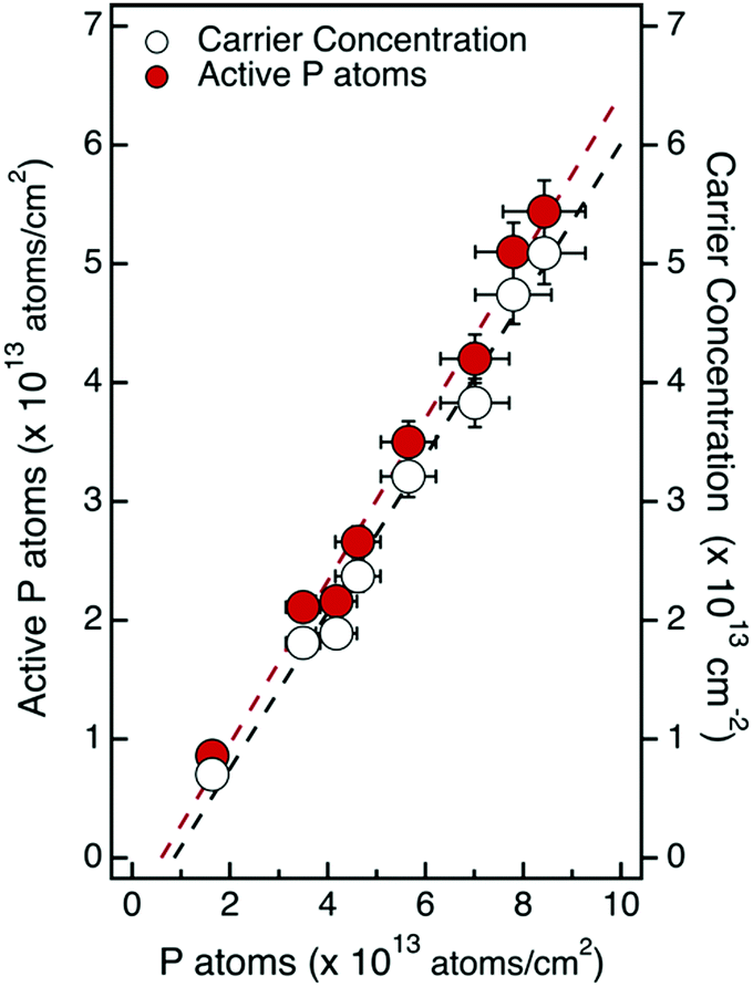 | ||
| Fig. 5 Carrier concentration and concentration of active P impurity atoms as a function of the ToF-SIMS dose of P atoms for the samples obtained by multiple grafting–O2 plasma ashing cycles. The concentration of active P impurity data was obtained from Hall effect measurements using a uniform layer approximation. The linear fits of the experimental data are indicated by dashed lines. | ||
To obtain information about the activation efficiency of the doping process, it is necessary to determine the ionization rate of the P atoms incorporated into the Si substrate. When P concentrations are higher than 1 × 1017 cm−3, only a fraction of the substitutional P impurity atoms incorporated into the Si crystal lattice is ionized, even at room temperature. Using the theoretical model of incomplete ionization proposed by Altermatt et al.,39 the ionization rate (ηi) was calculated for the different samples. Considering the free electron concentration determined by analysis of Hall measurements in constant doping approximation and the ionization rate ηi of the different samples, we determined the fraction of active P atoms in each sample. Fig. 5 reports the values of the active fraction of P atoms as a function of the ToF-SIMS dose of P atoms for the samples obtained by multiple grafting–ashing cycles. The linear fit of the experimental data provides an activation efficiency ηa = 69.3 ± 3.2%.
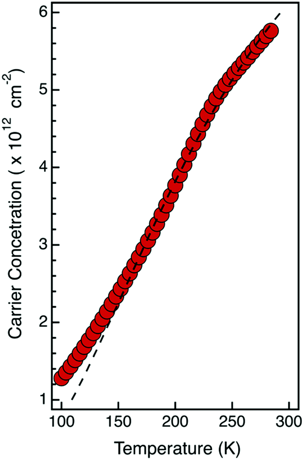
To countercheck the nature and concentration of the active dopant impurities, low temperature Hall measurements were performed on the sample obtained with a single grafting–ashing cycle and annealed at 1200 °C for 5 s. Acquisition temperatures were varied from 300 K to 100 K. Data acquired at different temperatures were analyzed using a constant doping approximation to determine the carrier concentration.9Fig. 6 reports the carrier concentration as a function of acquisition temperature. By fitting these data using the standard model reported by Gao et al.,23 we obtained the activation energy (Ea) and the concentration of active P impurity dopants (NA). In particular, the activation energy is compatible with the value Ea = 45 meV reported in the literature for phosphorus ionization in silicon.1 The concentration of electrically active P impurity dopants obtained from this analysis is NA = 9.4 × 1012 cm−2, corresponding to an ionization rate ηi = 85%. This value is perfectly consistent, within the experimental error, with the value ηi = 82% calculated for this sample, according to the theoretical model of incomplete ionization proposed by Altermatt et al.39
 | ||
| Fig. 6 Carrier concentration versus temperature obtained from Hall measurements at different T of a sample prepared with a single grafting–ashing cycle. Drive-in of the dopants was performed by annealing the sample in RTP at T = 1200 °C for 5 s. The black dashed line corresponds to the fitting of the data using the standard model reported in ref. 23. | ||
It is important to note that carrier concentration values obtained from Hall effect measurements using the uniform layer approximation are usually underestimated.26 Considering the high gradient of P concentration that is observed in ToF-SIMS depth profiles, a more accurate estimation of the effective carrier concentration requires determination of the Hall coefficient RH using a multilayer model that takes into account the variation of the dopant impurities and the associated variation of carrier mobility.9,23 On the basis of the ToF-SIMS depth profiles and assuming a Gaussian distribution of P impurity atoms, it is possible to correctly model the electron distribution in the Si substrate and calculate the effective carrier concentration in the samples. Following the same reasoning that was applied in the case of the uniform concentration approximation, the concentration of the active P impurity atoms was determined for the different samples. Fig. 7 reports the values of the active fraction of P atoms obtained using the multilayer model as a function of the ToF-SIMS dose of P atoms for the different samples. The linear fit of the experimental data provides an activation efficiency of ηa = 83.1 ± 3.6%.
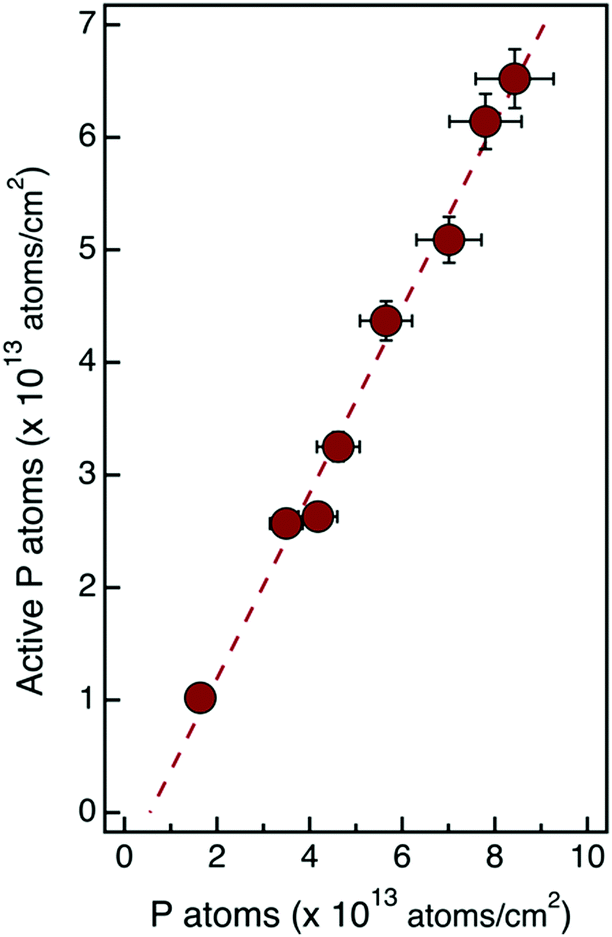 | ||
| Fig. 7 Concentration of active P impurity atoms as a function of the ToF-SIMS dose of P atoms for the samples obtained by multiple grafting–ashing cycles. The concentration of active P impurity atoms was obtained from Hall effect measurements using a multilayer model. Linear fit of the data (red dashed line) indicates an activation efficiency ηa = 83.1 ± 3.6%. | ||
Discussion
The main concern about doping strategies using self-assembling molecules is the presence of carbon and oxygen contamination and consequent dopant deactivation. P activation has been demonstrated to be almost full with no impact of carbon impurities.40 Conversely, recent results demonstrate that the presence of carbon contamination determines the formation of carbon–phosphorus pairs and the consequent deactivation of the P impurity atoms.23,38,40,41 In a previous experiment using MLD we demonstrated by means of combined ToF-SIMS and atom probe tomography (APT) analysis that carbon contamination is concentrated in a 2 nm thick layer close to the Si surface.42 A possible solution to overcome the problem of P deactivation determined by C contamination could be the removal of this contaminated layer by calibrated etching protocols. It is interesting to note that, in the case of MLD, high dose P junctions are characterized by relatively high activation efficiency.23 Conversely, carbon deactivation effect is particularly evident in the case of low dose P junctions. Activation efficiency as low as 7% has been reported for P junctions using super-branched poly-glycerol molecules.41 This effect can be tentatively attributed to the use of large molecules and consequently to the high level of carbon contamination that is introduced into the Si substrate during the annealing process for dopant drive-in. This fact suggests a limitation for MLD in terms of the effective capability to control P dose by changing the steric hindrance of the dopant containing molecules. Formation of the P dopant source on a native SiO2 layer can reduce the carbon contamination since carbon atoms are trapped at the SiO2/Si interface, reducing carbon diffusion in the doped substrate when carbon containing precursors are used. Nevertheless, the use of an oxide layer introduces severe limitation in the P drive-in process since high temperatures are necessary to overcome the SiO2 diffusion barrier, limiting the capability to control the junction depth.Alternatively, to reduce carbon injection into the substrate, it is necessary to remove the carbon containing molecule before drive-in of the P impurity atoms into the Si substrate. In a previous paper, we demonstrated that O2 and/or Ar plasma is extremely effective in removing the carbon component of the brush layer formed using homopolymers terminated with P-containing moieties.24 Accordingly, the level of carbon contamination in the dopant source is much lower than the one obtained using MLD with the same dopant containing moiety that is tethered to one end of the homopolymer chain.24 It is worth noting that the carbon content was determined to be of the order of adventitious carbon that is deposited over the sample substrate during exposure to air before deposition of the SiO2 capping layer. Moreover, the carbon content is independent of the P dose in the source i.e. of the molecular weight of the P terminated polymers or of the number of grafting-ashing cycles. Accordingly, in the present work, the dopant activation was found to be independent of P dose in the range of dopant concentrations that were explored, indicating that no significant P deactivation effects are induced by carbon contamination.
From a more general perspective it is important to compare these data with those reported in the literature in the case of a high concentration of P impurity atoms in the Si substrate by ion implantation. Activation has been a serious problem for the ion implantation technology. Post-annealing above 800 °C is commonly used for dopant activation43 and several thermal treatment schemes have been proposed to increase activation efficiency.44,45 Single step annealing at high temperature yields P activation of the order of 40–60%. Conversely, specific thermal treatments decoupling the damage recovery process and crystal regrowth from the electrical activation were demonstrated to significantly improve dopant activation. In 100 keV and 50 keV P implants, 100% and 75% activation of the implanted P atoms are reported, respectively, due to the different depth distributions of implantation damage in the Si substrate.44 In the case of high fluence low energy ion implantation, significant out diffusion of P impurity atoms is observed during annealing. This out diffusion process is associated with trapping of P at the SiO2/Si interface with consequent deactivation of the dopant impurities.46,47 The activation efficiency of P dopants close to the silicon surface is about 55–59%, due to the interaction with surface states and hydrogenation phenomena.47 Accordingly, the ∼80% activation efficiency in P junctions formed using the proposed self-assembly doping strategies are sufficiently high to compete with the current ion implantation technology. In this respect, we believe that the proposed technology represents a valuable alternative to ion implantation for all those applications requesting a simple and low cost approach to precisely control doping of silicon or other semiconductor materials. These layers of tethered P-terminated polymers represent a straightforward solution for the doping of nanostructured materials which cannot be processed using standard ion implantation due to shadowing phenomena, unless expensive and complex protocols are applied. Accordingly, we could envision the application of this technology for the doping of nanostructure substrates for photovoltaic applications, requiring effective approaches to reduce the cost of the devices.48
Finally, integration of self-assembly doping strategies with conventional lithographic protocols could provide the possibility of generating highly doped localized regions in Si overcoming the P concentration inducing the metal-semiconductor transition. Few experiments have been reported in the literature showing the possibility to localize grafting of dopant containing molecules in a small area with the lateral dimension of a few nanometers. These data indicate that self-assembly doping strategies could in principle pave the way towards mass fabrication of quantum dots, nanowires and sheets in the Si crystal. In turn, these elements could be used as building blocks for the fabrication of novel devices for quantum computation. Integration of P terminated polymers with advanced lithographic approaches is currently ongoing.
Conclusions
Polystyrene polymers with narrow molar mass distribution and end-terminated with a P containing moiety were grafted to a not-deglazed high resistivity Si substrate to build up a phosphorus δ-layer embedded in a SiO2 matrix. Subsequent drive-in of P atoms into the Si substrate was obtained by high temperature (1000–1250 °C) thermal treatments in RTP. Temperature-dependent resistivity and Hall measurements in the van der Pauw configuration were performed to investigate injection and activation of the P atoms into the Si substrate. High activation rates (ηa > 80%) of injected P atoms were achieved in the specific range of P concentrations explored in this work. According to these data, this bottom-up approach provides an effective doping technology that guarantees accurate control of the number of P atoms that are injected during the drive-in process into a semiconductor substrate. The high activation of the P atoms suggests this process could represent a valuable alternative to conventional ion implantation in samples that cannot withstand implantation induced crystal damage. Further experiments are currently investigating the integration of this doping approach with conventional lithography in order to control the lateral distribution of dopant containing molecules over the substrate at the nanoscale.Conflicts of interest
There are no conflicts to declare.Acknowledgements
The authors would like to thank Mario Alia (IMM-CNR) and Simone Cocco (IMM-CNR) for their help with clean room processes and electrical characterization of the samples, respectively.Notes and references
- S. M. Sze and K. K. Ng, Physics of Semiconductor Devices, John Wiley & Sons, Inc., 2007 Search PubMed.
- N. Sano and M. Tomizawa, Appl. Phys. Lett., 2001, 79, 2267 CrossRef CAS.
- T. Shinada, S. Okamoto, T. Kobayashi and I. Ohdomari, Nature, 2005, 437, 1128–1131 CrossRef CAS PubMed.
- P. A. Stolk, H.-J. Gossmann, D. J. Eaglesham, D. C. Jacobson, C. S. Rafferty, G. H. Gilmer, M. Jaráız, J. M. Poate, H. S. Luftman and T. E. Haynes, J. Appl. Phys., 1997, 81(9), 6031–6050 CrossRef CAS.
- J. O’Connell, G. A. Verni, A. Gangnaik, M. Shayesteh, B. Long, Y. M. Georgiev, N. Petkov, G. P. McGlacken, M. A. Morris, R. Duffy and J. D. Holmes, ACS Appl. Mater. Interfaces, 2015, 7, 15514–15521 CrossRef PubMed.
- C. Qin, H. Yin, G. Wang, Y. Zhang, J. Liu, Q. Zhang, H. Zhu, C. Zhao and H. H. Radamson, J. Mater. Sci.: Mater. Electron., 2020, 31, 98–104 CrossRef CAS.
- P. K. Chu, S. Qin, C. Chan, N. W. Cheung and L. A. Larson, Mater. Sci. Eng., R, 1996, 17, 207–280 CrossRef.
- M. L. Hoarfrost, K. Takei, V. Ho, A. Heitsch, P. Trefonas, A. Javey and R. A. Segalman, J. Phys. Chem. Lett., 2013, 4, 3741–3746 CrossRef CAS.
- J. C. Ho, R. Yerushalmi, Z. Jacobson, Z. Fan, R. L. Alley and A. Javey, Nat. Mater., 2008, 7, 62–67 CrossRef CAS.
- R. C. Longo, K. Cho, W. G. Schmidt, Y. J. Chabal and P. Thissen, Adv. Funct. Mater., 2013, 23, 3471–3477 CrossRef CAS.
- K. W. Ang, J. Barnett, W. Y. Loh, J. Huang, B. G. Min, P. Y. Hung, I. Ok, J. H. Yum, G. Bersuker, M. Rodgers, V. Kaushik, S. Gausepohl, C. Hobbs, P. D. Kirsch and R. Jammy, IEEE Int. Electron Devices Meet., 2011, 35.5.1–35.5.4 Search PubMed.
- J. C. Ho, A. C. Ford, Y. L. Chueh, P. W. Leu, O. Ergen, K. Takei, G. Smith, P. Majhi, J. Bennett and A. Javey, Appl. Phys. Lett., 2009, 95, 72108 CrossRef.
- J. H. Yum, H. S. Shin, R. Hill, J. Oh, H. D. Lee, R. M. Mushinski, T. W. Hudnall, C. W. Bielawski, S. K. Banerjee, W. Y. Loh, W.-E. Wang and P. A. Kirsch, Appl. Phys. Lett., 2012, 101, 253514 CrossRef.
- K. R. Kort, P. Y. Hung, P. D. Lysaght, W. Y. Loh, G. Bersuker and S. Banerjee, Phys. Chem. Chem. Phys., 2014, 16, 6539–6543 RSC.
- E. Y. J. Kong, P. Guo, X. Gong, B. Liu and Y. C. Yeo, IEEE Trans. Electron Devices, 2014, 61, 1039–1046 CAS.
- K. Cho, D. J. Ruebusch, M. H. Lee, J. H. Moon, A. C. Ford, R. Kapadia, K. Takei, O. Ergen and A. Javey, Appl. Phys. Lett., 2011, 98, 203101 CrossRef.
- B. Long, G. A. Verni, J. O’Connell, J. Holmes, M. Shayesteh, D. O’Connell and R. Duffy, Ion Implantation Technology, International Conference on Ion Implantation Technology 20th, 2014, 1–4.
- F. Sgarbossa, G. Maggioni, G. Andrea Rizzi, S. M. Carturan, E. Napolitani, W. Raniero, C. Carraro, F. Bondino, I. Píš and D. D. Salvador, Appl. Surf. Sci., 2019, 496, 143713 CrossRef CAS.
- F. Sgarbossa, S. M. Carturan, D. De Salvador, G. A. Rizzi, E. Napolitani, G. Maggioni, W. Raniero, D. R. Napoli, G. Granozzi and A. Carnera, Nanotechnology, 2018, 29(46), 465702 CrossRef CAS.
- N. Kennedy, R. Duffy, G. Mirabelli, L. Eaton, N. Petkov, J. D. Holmes, B. Long, C. Hatem and L. Walsh, J. Appl. Phys., 2019, 126, 025103 CrossRef.
- L. Ye, S. P. Pujari, H. Zuilhof, T. Kudernac, M. P. de Jong, W. G. van der Wiel and J. Huskens, ACS Appl. Mater. Interfaces, 2015, 7, 3231–3236 CrossRef CAS.
- M. L. Hoarfrost, K. Takei, V. Ho, A. Heitsch, P. Trefonas, A. Javey and R. A. Segalman, J. Phys. Chem. Lett., 2013, 4, 3741–3746 CrossRef CAS.
- X. Gao, B. Guan, A. Mesli, K. Chen and Y. Dan, Nat. Commun., 2018, 9, 118 CrossRef.
- M. Perego, G. Seguini, E. Arduca, A. Nomellini, K. Sparnacci, D. Antonioli, V. Gianotti and M. Laus, ACS Nano, 2018, 12, 178–186 CrossRef CAS PubMed.
- V. Gianotti, D. Antonioli, K. Sparnacci, M. Laus, C. Cassino, F. Marsano, G. Seguini and M. Perego, J. Anal. Appl. Pyrolysis, 2017, 128, 238–245 CrossRef CAS.
- R. Chiarcos, V. Gianotti, M. Cossi, A. Zoccante, D. Antonioli, K. Sparnacci, M. Laus, F. E. Caligiore and M. Perego, ACS Appl. Electron. Mater., 2019, 1(9), 1807–1816 CrossRef CAS.
- V. Gianotti, D. Antonioli, K. Sparnacci, M. Laus, T. J. Giammaria, F. Ferrarese Lupi, G. Seguini and M. Perego, Macromolecules, 2013, 46(20), 8224–8234 CrossRef CAS.
- K. Sparnacci, D. Antonioli, V. Gianotti, M. Laus, F. Ferrarese Lupi, T. J. Giammaria, G. Seguini and M. Perego, ACS Appl. Mater. Interfaces, 2015, 7, 10944–10951 CrossRef CAS PubMed.
- M. Mastromatteo, E. Arduca, E. Napolitani, G. Nicotra, D. De Salvador, L. Bacci, J. Frascaroli, G. Seguini, M. Scuderi, G. Impellizzeri, C. Spinella, M. Perego and A. Carnera, Surf. Interface Anal., 2014, 46, 393–396 CrossRef CAS.
- M. Perego, G. Seguini, A. Arduca, J. Frascaroli, D. De Salvador, M. Mastromatteo, A. Carnera, G. Nicotra, M. Scuderi, C. Spinella, G. Impellizzeri, C. Lenardi and E. Napolitani, Nanoscale, 2015, 7, 14469–14475 RSC.
- T. Gregorkiewicz and H. H. P. T. Bekman, Mater. Sci. Eng., B, 1989, 4, 291–297 CrossRef.
- L. Capello, I. Bertrand and O. Kononchuk, Phys. Status Solidi A, 2017, 214(7), 1700275 CrossRef.
- M. Mastromatteo, D. De Salvador, E. Napolitani, E. Arduca, G. Seguini, J. Frascaroli, M. Perego, G. Nicotra, C. Spinella, C. Lenardi and A. Carnera, J. Mater. Chem. C, 2016, 4, 3531–3539 RSC.
- M. Kuisl and E. Sasse, Thin Solid Films, 1980, 65, 373 CrossRef CAS.
- C. T. Sah, H. Sello and D. A. Tremere, J. Phys. Chem. Solids, 1959, 11(3), 288–298 CrossRef CAS.
- K. Shimakura, T. Suzuki and Y. Yadoiwa, Solid-State Electron., 1975, 18(11), 991 CrossRef CAS.
- A. Benninghoven, F. G. Ruedenauer and H. W. Werner, Secondary Ion Mass Spectrometry-Basic Concepts, Instrumental Aspects, Applications and Trends, Wiley, New York, 1987, vol. 86 Search PubMed.
- H. Wu, K. Li, X. Gao and Y. Dan, AIP Adv., 2017, 7, 105310 CrossRef.
- P. P. Altermatt, A. Schenk and G. Heiser, J. Appl. Phys., 2006, 100, 113714 CrossRef.
- J. Fu, K. Chen, S. Chang, K. Zhi, X. Gao, H. Wei and Y. Dan, AIP Adv., 2019, 9, 125219 CrossRef.
- H. Wu, B. Guan, Y. Sun, Y. Zhu and Y. Dan, Sci. Rep., 2017, 7, 41299 CrossRef CAS.
- Y. Shimizu, H. Takamizawa, K. Inoue, F. Yano, Y. Nagai, L. Lamagna, G. Mazzeo, M. Perego and E. Prati, Nanoscale, 2014, 6, 706–710 RSC.
- A. Shima and A. Hiraiwa, Jpn. J. Appl. Phys., 2006, 45, 5708 CrossRef CAS.
- N. Yu, K. B. Ma, C. Kirschbaum, K. Varahramyan and W. K. Chu, Appl. Phys. Lett., 1993, 63, 1125–1127 CrossRef CAS.
- T. Sameshima, K. Yasuta, M. Hasumi, T. Nagao and Y. Inouchi, Appl. Phys. A: Mater. Sci. Process., 2018, 124, 228 CrossRef.
- X. Zhang, D. Connelly, H. Takeuchi, M. Hytha, R. J. Mears, L. M. Rubin and T.-J. K. Liu, J. Vac. Sci. Technol., B, 2018, 36(6), 061211 CrossRef.
- S. J. Park, N. Uchida, H. Arimoto and T. Tada, Jpn. J. Appl. Phys., 2015, 54, 111302 CrossRef.
- R. A. Puglisi, C. Garozzo, C. Bongiorno, S. Di Franco, M. Italia, G. Mannino, S. Scalese and A. L. Magna, Sol. Energy Mater. Sol. Cells, 2015, 132, 118–122 CrossRef CAS.
| This journal is © The Royal Society of Chemistry 2020 |