 Open Access Article
Two-dimensional conjugated polymer films via liquid-interface-assisted synthesis toward organic electronic devices
Kejun
Liu†
,
Lihuan
Wang†
and
Renhao
Dong
 *
*
Faculty of Chemistry and Food Chemistry & Center for Advancing Electronics Dresden, Technische Universität Dresden, 01062 Dresden, Germany. E-mail: renhao.dong@tu-dresden.de
First published on 9th June 2020
Abstract
Conjugated polymers have received broad academic and industrial attention for optoelectronic applications. In contrast to linear (one-dimensional, 1D) conjugated polymers, the successive increase of dimensionality by covalently connecting multiple strands towards two-dimensional (2D) conjugated polymers (2DCPs) for organic electronics remains less explored. In this review article, we will summarize the current reports about 2DCPs through liquid-interface-assisted synthesis (LIAS), including Langmuir–Blodgett-assisted synthesis and liquid–liquid interfacial synthesis as well as surfactant-monolayer-assisted interfacial synthesis (SMAIS). Representative synthetic 2DCPs will be introduced, including graphyne, 2D conjugated covalent organic frameworks (2D c-COFs) and 2D conjugated metal–organic frameworks (2D c-MOFs), with emphasis on film synthesis by LIAS. Generally, these synthetic 2DCP films are intrinsic (semi-)conductors with tunable band gaps and possess high crystallinity, large-area, free-standing and single-/multi-layer features, which make processing and electronic device integration facile. To this end, we will discuss the application studies of 2DCP films in field-effect transistors (FETs), memristors and photodetectors, including the description of the device fabrication and unique performance. Finally, challenges and perspectives are provided regarding the future development of LIAS methods toward 2DCP films with diverse structural and functional control as well as the existing key questions for organic electronic devices.
1. Introduction
Linear (one dimensional, 1D) conjugated polymers, such as poly(p-phenylene), poly(p-phenylene vinylene), poly(acetylene), polypyrrole, polythiophene and polyaniline, possess continuous π-electron delocalization along the chain axis and have received broad academic and industrial interest.1–8 These conjugated polymers have exhibited many exciting properties, such as intrinsic optical and electronic activities, versatile doping/dedoping chemistry, flexibility, solution processability, light weight and low cost.3–8 Thus, the above unusual physical and chemical properties render conjugated polymers suitable for wide organic optoelectronic applications, including organic light-emitting diodes (OLEDs) for display and lighting applications, organic field-effect transistors (OFETs), organic photovoltaics (OPVs), organic radio frequency identification tags (ORFIDs) and organic spintronics.3–8Two-dimensional conjugated polymers (2DCPs) have been growingly accepted as crystalline, single- to few-layer polymer films/nanosheets via 2D covalent polymerization that exhibit strong in-plane π-electron delocalization along two orthogonal directions and weak out-of-plane π–π stacking.8–10 In contrast to the boosting development of linear conjugated polymers, the successive increase of dimensionality by covalently connecting multiple strands towards 2DCPs remains less explored. This is mostly because of the enormous synthetic challenges and limited available synthetic strategies of constricting long-range ordered polymerization in 2D while keeping structural control at the molecular level. Following early theoretical work on graphyne and 2D porphyrin polymers in the late 1980s to 1990s,11–13 describing how extending the dimensionality in the sense of translating the periodicity of conjugation affects the band structure, the HOMO–LUMO gap (HLG) contraction in 2DCPs generally becomes faster when increasing the oligomer size, while it slows down for the 1D case.14 This phenomenon was attributed to the number of conjugated links (k), which scales linearly with the oligomer length (n is the number of repeating units) in 1D (k = n − 1) but superlinearly in 2D  . As a result, the HLG of 2DCPs is always smaller than that of their 1D counterparts. Exceptionally, graphene, which can be considered as a naturally available 2DCP formed by strong carbon–carbon bonds, possesses extraordinary electronic, thermal, and mechanical properties, but nevertheless is a zero-bandgap material.15,16 In comparison with graphene, the electronic band gaps of synthetic 2DCPs can be finely adjusted by varying the monomers and conjugated connections at the molecular level. Another key advantage in an increased dimensionality of conjugated polymers is that the multiple strands offer multiple intramolecular pathways for charge carriers. Whereas in a 1D conductor a defect represents a bottleneck for the percolation of charges, in 2DCPs charge transport could be isotropic and bypass the possible defects.17
Towards the development of conjugated polymers in 2D directions, several synthetic strategies have been attempted so far. For instance, pioneering studies on 2D poly(m-phenylene) and covalent assemblies of porphyrin and thiophene as well as dynamic polyimine networks and metal–organic networks have been reported via on-surface synthesis under ultra-high vacuum conditions (UHV).14,18–23 However, the mobility of monomers on the surface is limited and only nano-scale domain sizes (tens of nanometers) have been obtained. As well, transfer of such metal surface-binding 2D polymers is a complicated issue, which has limited the further research of the electronic properties. Top-down exfoliation of synthetic laminar structures, such as layered conjugated 2D covalent organic frameworks (2D COFs) and 2D metal–organic frameworks (2D MOFs) as well as polymer crystals, has been successfully employed to achieve 2DCPs.24–28 However, the lateral sizes of the obtained 2DCP sheets are ultimately limited by the size of the single crystals, and the precise thickness control and unambiguous structural definition of the exfoliated nanosheets remain difficult so far. Recently, air–water and liquid–liquid interfaces have been explored towards the synthesis of 2DCP films.9,10,29–32 Such liquid-interface-assisted synthesis33 offers the possibility to overcome the limited diffusion speed of monomers, leading to macroscopic 2DCPs for which the interface acts as the template for the confined polymerization of monomers into 2D. For instance, we demonstrated the synthesis of imine-based 2DCPs at the air–water and liquid–liquid interfaces, which are free-standing, single- and few-layer polycrystalline films respectively.34 Moreover, such 2DCPs can be directly transferred from liquid interfaces to solid substrates (such as SiO2/Si wafers and boron nitride layers) for electronic device fabrication. Nevertheless, the crystallinity, i.e., long-range order degree of the covalently-bonded repeating units, of the resultant 2DCPs remains unsatisfactory with small crystalline domain sizes (10–20 nm). The synthesis of highly crystalline 2DCP films requires the development of new interfacial synthesis strategies, such as the surfactant-monolayer-assisted interfacial synthesis (SMAIS) method,35–38 and to address their synthetic mechanism, grain size (up to micrometer scale), grain boundaries and edge structures remains under development.
In this review article, we will introduce representative 2DCP films, such as graphyne,39,40 2D polymers,41,42 2D conjugated COF films (2D c-COF, a single-layer 2D COF is also regarded as a 2D polymer)43 and 2D conjugated MOF (2D c-MOF) films,44 through LIAS methods, including Langmuir–Blodgett-assisted synthesis and liquid–liquid interfacial synthesis as well as the SMAIS method recently developed by us. Then we will review the state-of-art development of 2DCP films enabled by LIAS toward logic, memory and photodetector devices. We will not comprehensively cover the literature; there are relevant reviews for various bulk 2DCP samples and multiple functions, such as separation, sensing, magnetics, electrocatalysis and energy storage.45–51 Our purpose is to provide a succinct summary of the LIAS strategies of previous work, and some pressing and important challenges, as well as a few 2DCP examples for organic electronic devices, which will be helpful for those interested in entering this exciting research area.
2. Developing LIAS methods toward 2DCPs
2.1. Langmuir–Blodgett-assisted 2D polymerization at the air–water interface
The air–water interface in a Langmuir–Blodgett (LB) trough has been employed to confine water-insoluble monomers into a pre-organized monolayer, which can be subsequently converted into 2DCP monolayers after a polymerization reaction.52 A general synthetic procedure toward 2DCP monolayers usually includes the following steps (Fig. 1): (1) a sub-monolayer of the first water-insoluble monomer is spread over the water surface in a LB trough; (2) after the close packing of the monomers into a dense film with highly ordered internal structure upon compression, a solution of the second monomer or metal salts is injected into the water phase; and (3) with the diffusion of the second water-soluble monomer or metal salts from the bulk phase to the interface, 2D polymerization is triggered, resulting in targeted single-layers with a large area (cm2). When one repeats the transfer process, layer-stacked 2DCPs can be prepared. Currently, this LB strategy has been successfully utilized for the synthesis of single-layer and multilayer 2DCPs.32,34,53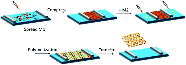 | ||
| Fig. 1 Schematic illustration of chemical synthesis at an air–water interface by the Langmuir–Blodgett (LB) method. | ||
In 2015, Schlüter and King et al. reported a free-standing, single-layer 2D polymer comprising C–C bonds at the air/water interface through photo-dimerization of anthracene-based amphiphilic monomers.54 Although the anthracene dimerization chemistry did not result in 2DCPs, their work was a milestone for the bottom-up interfacial synthesis of free-standing 2D polymers with defined structure, which inspired many following studies. An amphiphilic version of the shape-persistent antrip monomer was employed to self-assemble into a closely packed monolayer at the air/water interface. After a [4+4]-cycloaddition reaction upon UV light irradiation, a covalent monolayer sheet was achieved with a lateral size over 1 cm2 and a thickness of ∼1.2 nm, whose molecular-level resolved image was elucidated by scanning tunneling microscopy (STM).
The Schiff-base reaction, which forms a conjugated imine bond from the condensation between amine and aldehyde groups, has been widely applied in the synthesis of 2D and 3D COFs.55–57 Such a dynamic covalent reaction offers a promising protocol for the synthesis of 2DCPs at liquid interfaces. For instance, in 2016, Zhang and co-workers reported 2D polymerization between terephthalaldehyde and 1,3,5-trihexyl-2,4,6-tris(4-aminophenyl)benzene, yielding an organic thin layer (∼0.7 nm in thickness) at the air–water interface.58 At the same time, we achieved wafer-sized crystalline 2DCP monolayers with a thickness of 0.7 nm based on the condensation reaction of 5,10,15,20-tetrakis(4-aminophenyl)21H,23H-porphyrin-Co(II) and 2,5-dihydroxyterephthalaldehyde by LB-assisted interfacial synthesis (Fig. 2a).34 The achieved imine-based 2DP exhibited a macroscopically homogenous film with long straight edges of several hundred micrometers and a monolayer thickness of ∼0.7 nm (Fig. 2b). One remarkable feature of the resultant 2DP is that it displayed an outstanding Young's modulus (267 ± 30 GPa) comparable to that of graphene. The achieved 2DP could function as an active semiconducting layer in an organic thin film transistor (OTFT), whereas the 2DP employing the cobalt–porphyrin monomer could efficiently catalyze hydrogen generation from water.
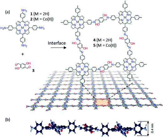 | ||
| Fig. 2 (a) Chemical structures of monomers (1, 2, and 3) and 2D polymers (4 and 5). (b) The cross-sectional view of the molecular structure of a monolayer 2DP (4) suggested by DFTB. Reproduced with permission from ref. 34. Copyright 2016 Nature Publishing Group. | ||
Another representative example is to synthesize large-area, single-layer 2D c-MOFs consisting of square-planar conjugated nickel bis(dithiolene) complexes at the air/water interface by LB-assisted interfacial synthesis.32 In this work, a π-conjugated monomer, named triphenylenehexathiol (THT), was employed to link with Ni for the formation of fully conjugated structure. Fig. 3a illustrates the typical synthesis process. After compressing the monomers into a monolayer on the water surface, a solution of nickel salts was injected into the water phase to trigger the coordination polymerization. The resultant 2D c-MOF could reach a large area on the order of cm2 (Fig. 3b), and a single-layer thickness of ∼0.7 nm (Fig. 3c). The obtained films exhibited a free-standing property and high mechanical strength, which could span over copper grids (Fig. 3d). As the single-layer sheets showed low stability under electron irradiation, selected area electron diffraction (SAED) was performed by cryogenic transmission electron microscopy (cryo-TEM) at −175 °C, exhibiting a typical hexagonal diffraction pattern (Fig. 3e, inset). This result at least suggests local crystallinity present in the single-layer 2D c-MOF with a hexagonal ordered network having a cell size of ∼2 nm. Such a 2D c-MOF was transferred onto glassy carbon electrodes for highly efficient electrocatalytic hydrogen generation. Due to their well-defined structure and abundant active sites as well as intrinsic conductivity, 2D c-MOFs have been rising as a promising electrocatalyst for electrochemical energy storage and conversion.
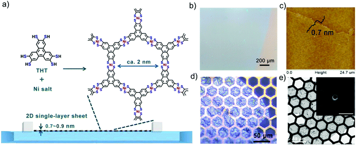 | ||
| Fig. 3 (a) Schematic illustration of the synthesis of a single-layer 2D c-MOF film by LB-assisted interfacial synthesis. (b) Optical microscopy (OM) image revealing a large-area monolayer. (c) AFM image. (d) OM image of the monolayer on Cu mesh. (e) TEM image. Inset: Selected area electron diffraction pattern of the monolayer. Reproduced with permission from ref. 32. Copyright 2015 John Wiley & Sons, Inc. | ||
2.2. Liquid–liquid interface assisted 2D polymerization
Besides the air–water interface, 2D polymerization can also be performed at the interface between two immiscible liquid layers, which provides a suitable 2D space to confine monomers and their subsequent polymerization to establish single- or multi-layers. Like the 2DCPs at the air–water interface, this method also provides the flexibility for easy transfer of 2DCPs onto any substrate for structural characterization and device fabrication. One typical example is to synthesize crystalline graphdiyne nanosheets from hexaethynylbenzene (HEB) via Glaser coupling at a dichloromethane–water interface at room temperature (Fig. 4a and b),59 which was reported by Nishihara et al. in 2017. In this work, HEB monomers were dissolved in dichloromethane while the copper(II) acetate catalysts were dissolved in water; the diffusion of the reactants at the liquid–liquid interface triggered the 2D-confined polymerization reaction. Compared with earlier work using liquid–solid interfaces, the LIAS method offered free-standing multi-layer (∼24 nm in thickness) graphdiyne nanosheets (Fig. 4c and d). The synthetic graphdiyne nanosheets exhibited regular hexagonal structure. Two-dimensional grazing-incidence wide-angle X-ray scattering (2D GIWAXS) and electronic diffraction (Fig. 4e) demonstrated an ABC-type stacking and a hexagonal lattice with in-plane and out-of-plane periodicities of a = b = 0.96 nm and c = 1.02 nm, respectively.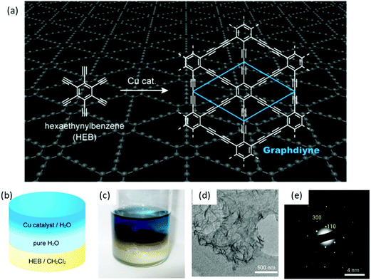 | ||
| Fig. 4 Liquid/liquid interfacial synthesis and microscopic observations of multilayer GDY. (a) Chemical reaction scheme of hexaethynylbenzene (HEB) to form GDY. (b) Schematic illustration and (c) the photograph of the reaction system. (d) TEM image and (e) SAED pattern of the GDY flakes. Reproduced with permission from ref. 59. Copyright 2017 American Chemical Society. | ||
The Banerjee group60 and Dichtel group61 as well as our group34 also employed the liquid–liquid interface strategy for the synthesis of large-area, free-standing 2DCP thin films. For example, Banerjee et al. developed a series of 2D polycondensation reactions through the Schiff-base reaction by involving 2,4,6-trihydroxybenzene-1,3,5-tricarbaldehyde (hydroxy aldehyde).60,62 As shown in Fig. 5a, the 2D polymerization can be divided into two steps: a reversible Schiff-base reaction to form amine compounds in the first step, and an irreversible enol-to-keto tautomerization process for yielding a stable keto-enamine compound in the second step. It is remarkable that the second step consumes the Schiff-base intermediates, which thereby drives the system towards the formation of 2DCPs. This chemical methodology even enables 2DCP formation in an aqueous system, which indicates the excellent stability of keto-COFs (Fig. 5b). As shown in Fig. 5c, these authors further modified these methodologies by introducing amine-p-toluene sulfonic acid (PTSA) salt to replace the free amine in the aqueous phase and dissolving the aldehyde in the dichloromethane organic phase.60 The PTSA–amine salt can slow the diffusion rate, which drove the reaction toward thermodynamically controlled crystallization at the liquid–liquid interface under ambient conditions. The synthesized 2DCP films possessed a thickness as low as sub-100 nm and exhibited high crystallinity which matches the proposed crystal structure well, as shown in Fig. 5d. Dichtel and co-workers also reported the synthesis of crystalline, free-standing 2DCP films via the interfacial polymerization of 1,3,5-tris(4-aminophenyl)benzene and terephthalaldehyde in a 1,4-dioxane/mesitylene mixed organic solvent layered on an aqueous solution containing a Lewis acid.61 This Lewis acid catalyst is highly water tolerant and accelerates imine formation so that polymerization is limited to the interface even when both monomers are dissolved in the organic phase. As a result, this method provided continuous films with the thickness controlled from 10 μm to 2.5 nm by varying the monomer concentration. The obtained 2DCP films were transferred onto polyethersulfone supports, and the resulting membranes showed enhanced rejection of Rhodamine WT for water purification.
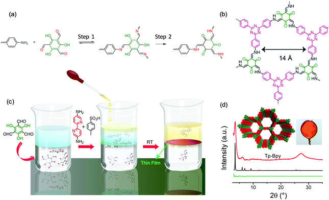 | ||
| Fig. 5 (a) The reaction mechanism of an amino monomer and 2,4,6-trihydroxybenzene-1,3,5-tricarbaldehyde. (b) Representative structures of one keto 2DCP. (c) Schematic illustration of the interfacial polymerization procedures. (d) XRD patterns of the 2DCP films compared with the calculated structures. Reproduced with permission from ref. 60. Copyright 2017 American Chemical Society. | ||
Recently, Park and Zhong et al. developed a novel liquid–liquid interfacial synthesis strategy, named laminar assembly polymerization (LAP),63 to prepare both porphyrin-based monolayer 2D polymers and 2D coordination polymers with wafer-scale homogeneity at a sharp pentane/water interface. As shown in Fig. 6a, after being delivered to the interface of pentane and water, the porphyrin-based monomers self-assembled at the interface with a face-on orientation. Fig. 6b illustrates the interfacial assembly process, which generated a laminar flow of the monomers away from the injection region and resulted in continuous monolayer assembly. The monomers stacked in an ordered monolayer and subsequently polymerized with metal ions or another organic ligand that were dissolved in the aqueous subphase (Fig. 6c). The coordinated 2D polymer monolayer comprising 5,10,15,20-(tetra-4-carboxyphenyl)porphyrin and Cu(II) is highly crystalline as characterized by XRD (Fig. 6d) and STM. Furthermore, the method allows the convenient fabrication of van der Waals heterostructures (vdWHs) composed of different 2D polymers and other 2D materials. Fig. 6e shows a representative multi-layer vdWH constructed by alternating one layer of a 2D polymer and three layers of molybdenum disulfide (MoS2), which can be used for vertical capacitor device arrays. However, the 2DCP linked by covalent bonds via the LAP method was still amorphous, which is unfavorable for superlattice formation in vdWHs. The above reports demonstrate that the liquid–liquid interfacial synthesis method exhibits powerful potential for the synthesis of monolayer- and multilayer-2DCPs but still requires improvement in controlled 2D polymerization.
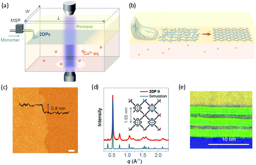 | ||
| Fig. 6 (a) Schematic of a laminar assembly polymerization (LAP) reactor and in situ optical characterization apparatus. MSP is a micro-syringe pump. (b) Schematic illustration of the LAP synthesis, which involves three phases. (c) AFM height image of the monolayer 2D polymer. (d) Experimental and calculated in-plane XRD profiles for the coordinated 2D polymer. (e) A cross-sectional annular dark field (ADF) scanning transmission electron microscopy (STEM) image of a 2D polymer/(MoS2)3 superlattice film transferred onto a SiO2/Si-substrate. Carbon (yellow) and oxygen (blue) EELS mapping and ADF STEM signal (green). Reproduced with permission from ref. 63. Copyright 2019 American Association for the Advancement of Science. | ||
2.3. Surfactant-monolayer-assisted interfacial synthesis (SMAIS)
Despite the great success in the controlled synthesis of 2DCPs with tunable layer numbers via LB-assisted and liquid–liquid interface assisted synthesis, the crystallinity of these developed 2DCPs remained unsatisfactory with small crystalline domain sizes of 10–50 nm and defective structures, and the understanding of on-water surface synthesis remains poor.Very recently, we reported the synthesis of few-layer 2D polyimide and 2D polyamide crystals at the air–water interface, through a reaction between amine and anhydride monomers, assisted by surfactant monolayers.35 Surfactants are typical amphiphilic molecules, which can preferentially adsorb at the air–water interface with the hydrophobic tails toward the air while the hydrophilic heads face the water, and closely stack to form highly ordered layers.64 Thus, we expect that the surfactant layer can guide the supramolecular self-assembly of monomers on its hydrophilic side via weak interactions (such as hydrogen bonds, electrostatic interactions, and van der Waals forces), and further provides a 2D confinement geometry for the polymerization into 2D. A general procedure can be described as follows (Fig. 7): (1) surfactant molecules are firstly spread at the air–water interface and closely stack into a single layer; (2) an aqueous solution of the first monomer is injected into the water phase and subsequently the monomers self-assemble underneath the surfactant monolayer via non-covalent interactions such as electrostatic forces, hydrogen-bonding, and coordination interactions; (3) the second monomer or the catalyst is added to trigger the in situ 2D polymerization guided by the surfactant monolayer; and (4) the 2DCP films have a thickness of only a few nanometers and can be readily transferred onto arbitrary substrates, opening up exciting opportunities for the integration of 2DCPs into next-generation devices and systems. The surfactant molecules can be readily removed by organic solvents (i.e., chloroform, alcohol).
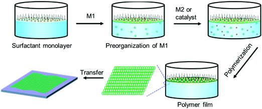 | ||
| Fig. 7 Schematic illustration of the surfactant-monolayer-assisted interfacial synthesis (SMAIS) method toward 2DCP films. M1: monomer 1 (green ball). M2: monomer 2 (red ball). | ||
In our work, a chloroform solution of sodium oleic sulfate SOS was first spread at the air–water interface.35 With the evaporation of chloroform, the SOS molecules self-assembled into a monolayer with –SO4− polar head groups toward the water phase. Then an aqueous solution of 5,10,15,20-tetrakis(4-aminophenyl)porphyrin (monomer 1, 1 mL, 1 mg mL−1 in 0.12 M HCl solution) was injected into the water phase at room temperature. Due to hydrogen bonding and electrostatic interactions, the protonated monomers could be readily adsorbed underneath the SOS monolayer. In the next step, deprotonated perylenetetracarboxylic dianhydride (monomer 2, 0.64 mL, 1 mg mL−1 in 0.08 M LiOH aqueous solution) was added to the water phase and diffused to the interface where polymerization was triggered with the formation of imide bonds. The interfacial reaction was kept at room temperature for 7 days to provide a highly crystalline 2D polyimide (2DPI) film (Fig. 8a). The synthetic 2DPI films exhibited a large area with lateral size up to several cm2, a thickness of approximately 2 nm (corresponding to ∼5 layers), and an average crystal domain size of around 3.5 μm2. The 3 nm lattice of 2DPI can be clearly revealed by selected area electronic diffraction (SAED, Fig. 8b) and high-resolution TEM (HRTEM) imaging (Fig. 8c). Nevertheless, the crystalline area (vs. amorphous region) is below 70% of the whole film. In addition, the reaction time is too long (a few days) due to the possible low reactivity of monomers on the water surface. We further extended this SMAIS strategy to the polycondensation reaction of porphyrin monomer 1 and 1H,3H-furo[3,4-f][2]benzofuran-1,3,5,7-tetrone, providing a crystalline few-layer 2D polyamide (2DPA) with dual-pore lattice structures (Fig. 8b). Under the SOS monolayer, 2DPA adopted a face-on configuration with a crystal domain size of ∼0.3 μm2. By utilizing an octadecanoic acid (stearic acid, SA) monolayer, we achieved edge-on-oriented 2DPA with significantly increased domain size (∼121 μm2). The molecular structures of the polymers and the role of the surfactants were investigated by grazing-incidence wide-angle X-ray scattering (GIWAXS) and aberration-corrected high-resolution transmission electron microscopy (AC-HRTEM) with the support of theoretical modelling. Our results indicate that the surfactant, depending on its polar head, promoted the arrangement of the monomers – and in turn their polymerization – either horizontally or vertically with respect to the water surface, which is also helpful for controlled synthesis with directional layer orientation.
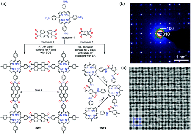 | ||
| Fig. 8 Synthesis protocol of 2D polymers. (a) A reaction scheme illustrating the synthesis of 2DPi and 2DPA via condensation reactions, with the assistance of surfactant monolayers on the water surface. (b) SAED pattern of 2DPI. (c) HRTEM image of 2DPI with an inserted simulated image on the left side. Reproduced with permission from ref. 35. Copyright 2019 Nature Publishing Group. | ||
To further explore the potential of SMAIS, crystalline quasi-2D polyaniline films were also synthesized with a lateral size of ∼50 cm2 and tunable thickness (2.6–30 nm).36 The superior charge transport properties and chemiresistivity toward ammonia and volatile organic compounds render the quasi-2D polyaniline films promising electroactive materials for thin-film organic electronics. In our newest results, we also extended the SMAIS method to imine-based 2DCP thin films. Besides the generality in the synthesis of 2DCP films, compared with the LB method and liquid–liquid interfacial method,34 the SMAIS approach was found to render the 2DCP higher crystallinity. For instance, we synthesized three porphyrin and triazine containing polycrystalline multilayer imine-based 2DCP films with square and hexagonal lattices, respectively.38 Typically, the synthetic 2D polyimine films from SMAIS featured polycrystalline multilayers with tunable thickness from 6 to 200 nm and large crystalline domains (100–150 nm in size), which were one order of magnitude larger than the previously reported 2D polyimine.34 Furthermore, it is to be noted that the resultant 2D polyimine film was fully crystalline in the presence of a Lewis acid catalyst (ytterbium(III)-trifluoromethanesulfonate, Yb(OTf)3), i.e., the amorphous region was eliminated. As a result, the extended conjugation of the porphyrin moieties within a 2D layer together with the high crystallinity makes this 2DCP an attractive material for the fundamental investigation of charge carrier transport properties (discussed in Section 3.1). In our later report, crystalline boronate ester-based 2DCPs composed of porphyrin macrocycles and phenyl or naphthyl linkers were achieved by the SMAIS method on the water surface.37 The achieved 2DCPs were free-standing thin films with tunable thickness from 6 to 16 nm and large single-crystalline domains up to ∼60 μm2, which are much larger than those of thus-far reported boronate ester-based 2D polymers (both film and powder samples). Benefiting from the high crystallinity and thin-film processability with controlled film thickness as well as the intrinsic semiconducting feature, the above 2DCPs have been incorporated into thin-film logic and memory devices, which will be introduced below.
3. Bringing 2DCPs toward logic devices
Next, we will discuss recent progress on integrating 2DCP films enabled by LIAS, including representative 2D polymers, 2D c-COF films and 2D c-MOF films, into logic and memory devices including FETs, photodetectors and resistive memories. In these electronic devices, with the input or output of current or voltage, a 2DCP layer will enable a function as data storage or logic processing. We will try to highlight the diversity of roles that 2DCPs can play in these electronic devices and provide understanding about the structure–performance relationship.3.1. 2D COF/2D polymer films for FETs
In 2005, the Yaghi group reported a layer-stacked crystalline 2D COF composed of repeating benzene rings linked by boroxine.65 Typically, 2D COFs are formed by strong in-plane covalent bonding and weak out-of-plane van der Waals forces. Since then, more than one hundred 2D COFs have been developed employing abundant organic building blocks and rich linkage chemistries, such as imine, boronate, hydrozone, azine, squaraine, pyrazine, imide, benzimidazole and triazine linkages as well as carbon–carbon bonds.46 Due to their structural diversity, high chemical/thermal stability, porosity and crystallinity, 2D COFs have attracted considerable attention for potential applications in gas storage,66,67 separation,60,61,68,69 catalysis,70–72 sensing,73,74 proton conductors,75–77 optics,78 magnetics,79–82 and energy conversion83 and storage.84–89During the last decade, 2D COFs have been rising for (opto-)electronics due to the intrinsic π-conjugated structures. However, most 2D COFs showed extremely low conductivity of <10−10 S cm−1, which has largely limited their electronic applications. In 2008, Jiang and co-workers reported a boronic ester TP-COF with pyrene moieties in the backbone through the polymerization of pyrene-2,7-diboronic acid and 2,3,6,7,10,11-hexahydroxytriphenylene (HHTP), which showed a p-type semiconducting behavior.90 The I–V profile of the TP-COF showed a current of 4.3 nA at a 2 V bias voltage compared to only 79 pA for a sample composed of the COF precursors. After that, improved charge transport properties in 2D COFs have been further achieved by integrating photoconductive π-conjugated building blocks into the backbones, such as pyrene, thiophene, tetrathiafulvalene, porphyrin, hexabenzocoronene, and phthalocyanine,91–96 or by employing conjugated linkages such as carbon–carbon bonds26,82,97 and pyrazine units,74,98,99 which rendered 2D c-COFs a new generation of organic semiconductors (Table 1).34,100–103 Till now, various p-, n- and ambipolar-type 2D c-COFs have been established with fine tuning of their band gap ranging from 0.5 eV to 2.5 eV45,82,90,93,100,103–124 and an intrinsic electrical conductivity of 10−10–10−6 S cm−1 in their pellet form.125 Upon doping with TCNQ or I2, the conductivity value could reach as high as ∼3 × 10⁻³ S cm−1 (Table 1).82,119
| Material | Sample type | Method | σ/S cm−1 | μ/cm2 V−1 s−1 | Ref. |
|---|---|---|---|---|---|
| Note: σ, conductivity at room temperature; μ, charge mobility.a Mobility measurements: by FET devices.b By flash photolysis time-resolved microwave conductivity (FP-TRMC) technology.c By the Hall effect.d By THz technology. “—” Not reported. | |||||
| 2D polyimine (LB) | Monolayer | — | — | 1.3 × 10⁻⁶ (h)a | 34 |
| 2D polyimine (SMAIS) | Few layer | — | — | 0.01 (h)d | 38 |
| COF-DC-8 | Pellet | 4-Probe | 2.5 × 10⁻⁵ | — | 74 |
| sp2c-COF | Pellet | 2-Probe | 6.1 × 10⁻¹⁶ | — | 82 |
| sp2c-COF/I2 | Pellet | 2-Probe | 6.1 × 10⁻⁴ | — | 82 |
| 2D polyimide | Film | — | ∼1.0 × 10⁻⁶ | 4.3 × 10⁻³ (h)a | 87 |
| COF-366 | Pellet | — | — | 8.1 (h)b | 93 |
| COF-66 | Pellet | — | — | 3.0 (h)b | 93 |
| HBC-COF | Pellet | — | — | 0.7 (h)b | 95 |
| polyTB | Few layer | — | — | 3.0 × 10⁻⁶![[thin space (1/6-em)]](https://www.rsc.org/images/entities/char_2009.gif) a a |
96 |
| CS-COF | Pellet | — | — | 4.2 (h)b | 98 |
| BDT-COF | Film | — | ∼5.0 × 10⁻⁷ | ∼3.0 × 10⁻⁷ (h)a | 106 |
| 1-S | Pellet | 2-Probe | ∼3.7 × 10⁻¹⁰ | — | 112 |
| 1-Se | Pellet | 2-Probe | ∼8.4 × 10⁻⁹ | — | 112 |
| 1-Te | Pellet | 2-Probe | ∼1.3 × 10⁻⁷ | — | 112 |
| NiPc COF | Pellet | — | — | 1.3 (h)b | 113 |
| TTF-Ph-COF | Pellet | 2-Probe | 10−5 | 0.2 (h)b | 115 |
| TTF-Py-COF | Pellet | 2-Probe | 10−6 | 0.08 (h)b | 115 |
| TANG-COF/I2 | Pellet | 4-Probe | ∼2.0 × 10⁻³ | 116 | |
| TTF-COF/I2 | Pellet | 2-Probe | 1.8 × 10⁻⁶ | — | 117 |
| TTF-COF/I2 | Film | 2-Probe | 2.8 × 10⁻³ | — | 119 |
| TTF-COF | Film | 2-Probe | 1.2 × 10⁻⁶ | — | 119 |
| ZnP-COF | Pellet | — | — | 0.016 (e),b 0.032 (h)b | 121 |
| CuP-COF | Pellet | — | — | 0.19 (e)b | 121 |
| H2P-COF | Pellet | — | — | 3.5 (h)b | 121 |
| 2D D-A COF | Pellet | — | — | 0.04 (e),b 0.01 (h)b | 122 |
| 2D-NiPc-BTDA COF | Pellet | — | — | 0.6 (e)b | 123 |
| CuPc-pz COF | Pellet | Van der Pauw | 3.3 × 10⁻⁷ | 0.9 ± 0.2 (h),c 0.7 (h)d | 125 |
| ZnPc-pz COF | Pellet | Van der Pauw | 7.0 × 10⁻⁷ | 4.8 ± 0.7 (h),c 2.0 (h)d | 125 |
| 2DPTTI | Few layer | — | — | 1.37 × 10⁻³ (h)a | 128 |
Recently, we introduced two novel pyrazine (pz)-linked metal-phthalocyanine (MPc)-based 2D c-COFs (MPc-pz, M = Zn or Cu).125 The MPc-pz materials were synthesized by condensation of 2,3,9,10,16,17,23,24-octaamino-phthalocyaninato metal[II] (OAPcZn or OAPcCu) and tert-butylpyrene-tetraone (tBu-PT) via a solvothermal method (Fig. 9a). The resultant materials were polycrystalline p-type semiconductors with calculated band gaps of ∼0.6 eV. The Hall effect, the Van der Pauw method, time-resolved terahertz spectroscopy and density functional theory calculations were employed for characterizing the intrinsic and extrinsic factors determining the electronic properties of these 2D c-COFs. We demonstrated that for this p-type semiconductor, changing the metal center from Cu to Zn in the phthalocyanine moiety had a negligible effect on the room-temperature conductivity (∼5 × 10⁻⁷ S cm−1) charge density (∼1012 cm−3), charge carrier scattering rate (∼3 × 10¹³ s−1), and effective mass (∼2.3 m0) of majority carriers (holes). When compared to the state-of-the-art reports of semiconducting COF samples, a record device-relevant mobility up to ∼5 cm2 V−1 s−1 was resolved in the dc limit, which was limited by long-range charge carrier transport across crystalline grain boundaries in the pellet form (Fig. 9d). Both samples revealed a typical semiconducting drop of the conductivity upon sample cooling (Fig. 9e), with almost identical activation energies for both samples (0.34 ± 0.1 eV). Notably, the charge transport was found to be highly anisotropic, with the hole mobilities being practically null in-plane and finite out-of-plane for the developed 2D c-COFs (Fig. 9b and c). This work highlighted the potential of high mobility 2D c-COFs as semiconductors for (opto-)electronics and provided a rational approach to ascertain structure–property relationships, revealing that a detailed analysis of the conductivity might offer a reliable path for designing and developing semiconducting COF materials with improved charge transport properties.
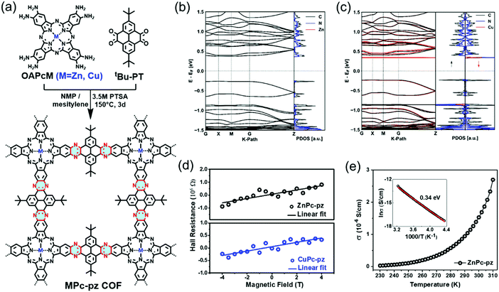 | ||
Fig. 9 (a) Schematic illustration of the synthesis of MPc-pz 2D c-COFs. (b and c) Electronic band structures (left panel) and projected density of states (PDOS) (right panel) of serrated AA stacked multilayers of ZnPc-pz and CuPc-pz, respectively. (d) Hall effect measurements at 300 K. (e) Variable-temperature electrical conductivity of ZnPc-pz via the van der Pauw method. The insert is the plot of the natural logarithm of conductivity (ln![[thin space (1/6-em)]](https://www.rsc.org/images/entities/char_2009.gif) σ) as a function of inverse temperature (1000/T). Reproduced with permission from ref. 125. Copyright 2019 American Chemical Society. σ) as a function of inverse temperature (1000/T). Reproduced with permission from ref. 125. Copyright 2019 American Chemical Society. | ||
Despite the promising electronic properties, the electronic devices integrated with these insoluble bulk 2D c-COF powders often exhibit lower efficiency than expected, due to challenges in device processing and the heterogeneous feature arising from the inter-particle interactions, disordered stacking, crystalline grain boundaries and defects. LIAS has provided a pathway to prepare large-area thin films of 2D c-COFs with long-range ordered structures and tailored thickness.9,10,58,60,61,126 In 2015, Bao and co-workers reported a large-area 2D polyimine film (consisting of a BDT core bearing extended alkoxy chains and triphenylamine) with varied thickness from ∼2 to 150 nm at a dimethylformamide (DMF)/air interface.96 This polyimine thin film was transferred to a Si wafer with a 300 nm oxide layer. Then, 40 nm thick Au source and drain top contacts were deposited through a shadow mask, defining a top-contact transistor with a channel length and width of 50 and 4000 μm, respectively. Upon applying an additional gate voltage, the source–drain current rose by two orders of magnitude. A charge carrier mobility of 3.0 × 10⁻⁶ cm2 V−1 s−1 and an average on/off ratio of 850 were achieved. In 2016, we employed a LB-assisted interfacial synthesis method and synthesized a wafer-sized crystalline monolayer (∼0.7 nm in thickness) 2D polyimine film (Fig. 2 and 10a and b).34 Then, the monolayer 2D polyimine was integrated into a thin-film transistor for a proof-of-concept demonstration of the achieved 2DCP as an active semiconducting layer. The 2D polyimine film was horizontally transferred onto an n-doped Si wafer with a 300 nm SiO2 layer (dielectric), on which 30 nm thick gold was deposited and used as bottom electrodes. From the transfer curve (Fig. 10c), a mobility of 1.3 × 10⁻⁶ cm2 V−1 s−1 and an on/off ratio of 102 were obtained. When the 2D polyimine was doped with I2, the charge carrier mobility increased by a factor of more than two orders of magnitude and reached 1.6 × 10⁻⁴ cm2 V−1 s−1 (Fig. 10d). The above two reports show that the developed single- and few-layer 2DCP films enabled by LIAS have the potential to be used as semiconducting components for thin-film transistors (TFTs). The relatively low mobilities of these polyimine transistors may be attributable to low π-conjugation through imine bonds, low crystallinity in the thin film and possible defects. As mentioned above, we recently employed the SMAIS method for the synthesis of few-/multi-layer 2D polyimine films with large crystalline domains (100–150 nm in size).38 Intrigued by the high crystallinity and the presence of electroactive porphyrin moieties, the optoelectronic properties of the 2D polyimine films are investigated by time-resolved terahertz spectroscopy. Typically, the porphyrin-based 2D polyimine film exhibited a p-type semiconductor behavior with a band gap of 1.38 eV and hole mobility as high as 0.01 cm2 V−1 s−1, superior to the previously reported polyimine based materials. In contrast, the amorphous 2D polyimine film synthesized without a surfactant on the water surface failed to generate photoconductivity during the THz spectroscopy measurements. These results suggest that long range ordered structures are essential to enhance charge transport. Nevertheless, the controlled synthesis of single- or multi-layer films with high crystallinity as well as fine-tuned lateral size and thickness is still a critical issue for boosting their device performance.
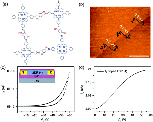 | ||
| Fig. 10 (a) Chemical structures of 2D polyimine. (b) AFM image of a monolayer. (c) Transfer curve of a thin film transistor at a source to drain voltage of −40 V. (d) Transfer curve of iodine-doped 2D polyimine in the FET device. Reprinted with permission from Macmillan Publishers Ltd: Nat. Commun., ref. 34, copyright 2016. | ||
Inspired by the progress achieved so far, the high crystallinity and close layer stacking alignment of aromatic moieties as well as in-plane extended π-electron delocalization render 2D c-COF films or 2D polymer films ideal platforms for charge carrier transport. Besides the LIAS methods, great effort has been dedicated to controlled synthesis for bringing semi-conducting 2D COFs into logic devices. For example, Xu et al. reported the synthesis of few-layer crystalline 2D polyimide nanosheets through the hydrogen-bond-induced preorganization of pyromellitic acid and melamine followed by the imidization reaction of the obtained planar hydrogen-bonded networks (Fig. 11a).87 The obtained 2D polyimide nanosheets showed an average lateral size of ∼4 μm and a thickness of 1.5–2.6 nm (Fig. 11b). HR-TEM imaging certified the high crystallinity and hexagonal 2D crystal structures with long-range order (Fig. 11c). Moreover, the resultant nanosheets presented excellent dispersibility in ethanol in the long term (>2 months), which provided solution processability for FET device fabrication. To this end, a typical transfer curve (IDSvs. VG with VDS = 1 V) of the 2D polyimide-based FET device showed a p-type behavior with an on/off ratio of 1.4 × 10⁴, and a mobility of 4.3 × 10⁻³ cm2 V−1 s−1. Here, besides the difference in the chemical components, the largely improved mobility values in this 2D polyimide compared to those in the above 2D polyimines (10−6 cm2 V−1 s−1) benefited from its high sample crystallinity and homogeneous features, which generate a high-quality interface between the semiconductor, SiO2 dielectric and source/drain electrodes.
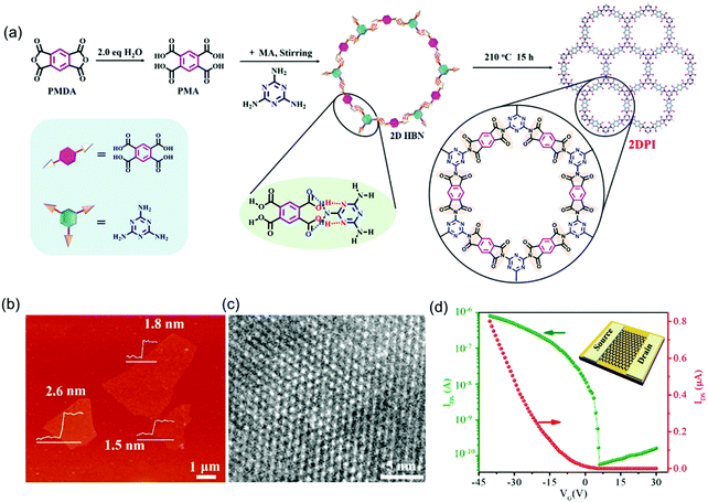 | ||
| Fig. 11 (a) Solvothermal synthesis of 2D polyimide nanosheets. (b) AFM image. (c) HRTEM image. (d) Transfer curve of the 2D polyimide-based FET device (VDS = 1 V). Reproduced with permission from ref. 87. Copyright 2019 American Chemical Society. | ||
Recently, C–C bonding via coupling reactions – for example, the Suzuki reaction – has attracted extensive attention for the synthesis of 2DCPs by the LIAS method.127,128 C–C bond based 2DCPs are expected to exhibit high charge mobility due to the extended conjugation length. In addition, the robust C–C bonds render 2DCPs high chemical stability against treatment with strong acid/base solutions. In the latest work from Hu and Dong et al.,128 a C–C bond based 2DCP – termed polytriethyltriindole (2DPTTI) – can be synthesized via a Suzuki reaction at a liquid–liquid interface in the presence of a Pd[0] catalyst and base (Fig. 12a). The reaction can be divided into two phases (Fig. 12b): the bottom aqueous phase containing the inorganic base (NaOH) and the upper organic phase (toluene) containing the Pd catalyst and monomers, including 2,7,12-tribromo-5,10,15-triethyltriindole (2-BrTTI) and 1,4-benzenediboronic acid dipinacol ester (BADE). The AFM measurement (Fig. 12c) shows that the obtained film is a flat mm-sized thin sheet without cracks, which reveals 2.5 nm thickness. The thickness of the resultant 2DPTTI could be varied from 2.5 nm to 46.0 nm by controlling the reaction time. XRD and SAED results confirm the high crystallinity with hexagonal structure and a layer-stacked feature. To explore the function of 2DPTTI films in electronic devices, polymer field-effect transistors (PFETs) were fabricated with a bottom-gate top contact device geometry on a Si/SiO2 (300 nm) substrate and a top light illumination mode for phototransistors (Fig. 12d). Fig. 12e and f present typical transfer and output curves of the 2DPTTI-based device, respectively, which display p-type charge transport. Efficient charge injection between the 2DPTTI film and the source/drain electrode was proved as indicated by the linear character in the output curves. Those devices can exhibit a low threshold voltage (VT; lower than 10 V), and a high current on/off ratio of 5.0 × 10³ with a saturation charge carrier mobility of up to 1.37 × 10⁻³ cm2 V−1 s−1. The extended π-conjugation in 2D ensures an isotropic charge transport property, which is important for large-area device applications.
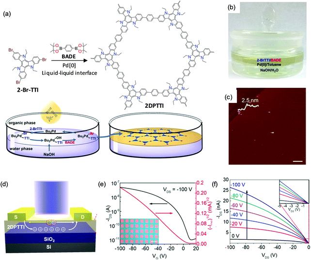 | ||
| Fig. 12 (a) Synthesis of 2D polytriethyltriindole (2DPTTI) via a Suzuki reaction between 2-BrTTI and BADE monomers at liquid–liquid interfaces. (b) Photograph of the setup for interfacial synthesis of the 2DPTTI film. (c) AFM image of 2DPTTI revealing a thickness of 2.5 nm. (d) 2DPPTI-based polymer field-effect transistor and phototransistor. (e and f) Representative transfer and output curves of 2DPTTI-based transistors. The inset in (e) is the optical microscopy image of the constructed 2DPTTI transistor arrays (scale bar: 100 μm) and the inset in (f) is enlarged output curves at low voltage. Reproduced with permission from ref. 128. Copyright 2020 John Wiley & Sons, Inc. | ||
3.2. 2D c-MOF films for FETs
Conventional 3D MOFs are regarded as insulators (<10−8 S cm−1) due to the large separation of metal centers by multiple atoms, insulating organic ligands, etc., which has limited their applications in electronics.51,129 In 2009, Kitagawa et al. reported a highly conducting Cu[Cu(pdt)2] (pdt = 2,3-pyrazinedithiolate) sample with a conductivity value of 6 × 10⁻⁴ S cm−1 at 300 K.130 Moreover, the doping of guest molecules (such as I2 and 7,7,8,8-tetracyanoquinododimethane) in the frameworks could lead to an increased electrical conductivity by several orders of magnitude.129 Gu et al. reported a Cu3BTC2 MOF (BTC = 1,3,5-benzene tricarboxylate) thin film for OFETs.131 The MOF thin film was firstly prepared by a liquid-phase epitaxial approach to modify the SiO2/Si substrate. A thiophene-based semiconducting polymer of PTB7-Th was coated on the MOF film surface, followed by two top Au electrodes on the semiconducting film. This SURMOF/polymer-based OFET exhibited a hole mobility of ∼1.0 × 10⁻² cm2 V−1 s−1, an on/off ratio of 103 and a threshold voltage less than 10 V. This performance was superior to that of an OFET without SURMOF as a coating layer (average hole mobility of ∼5.0 × 10⁻³ cm2 V−1 s−1 and threshold voltage larger than 13 V). The performance enhancement was mainly attributed to the highly crystalline, homogeneous, and low-k SURMOF grown on the SiO2/Si substrate and the smaller interface trap density in the OFET. However, it was challenging to realize high-mobility semi-conductive MOFs for logic electronics.132Recent advances disclosed that the designs of 2D c-MOFs, which refer to layer-stacked MOFs comprising planar ligands and linkages with high in-plane conjugation and weak out-of-plane van der Waals interactions, have led to largely improved conductivity (>0.1 S cm−1).9,10,48,50,133 In 2013, Yaghi et al.134 reported fully π-d conjugated, graphene-like 2D MOF crystals comprising Cu-catecholates (HHTP-Cu), which showed conductivity as high as ∼0.2 S cm−1. Since then, it has been commonly accepted that the development of highly conductive 2D MOFs strongly relies on the design of planar linking units and organic ligands for the construction of a π-d conjugated system. So far, various types of 2D c-MOFs have been synthesized based on phenylene,31 triphenylene,32,44 phthalocyanine,135,136 coronene137,138 and dibenzo[g,p]chrysene139 derivatives with functional groups (–OH, –NH2, –SeH or –SH). They displayed superior electrical conductivity values of 40, 160 and 1580 S cm−1 in 2D c-MOF films of hexaiminotriphenylene-Ni (HITP-Ni),140 hexathiolatedbenzene-Ni (HTB-Ni)141 and hexathiolatedbenzene-Cu (HTB-Cu),142 respectively. These materials have been integrated as electrode materials for applications in electrocatalysis,32,136,143–149 chemiresistive sensors,150–155 energy storage33,156–162 and superconductivity.163
However, the integration of 2D c-MOFs into highly efficient electronic devices remains challenging due to the difficulty in processing the powder samples. In 2013, Nishihara et al. synthesized a multi-layer, crystalline HTB-Ni film with a lateral size of ∼100 μm and a thickness of 1–2 μm at a H2O/CH2Cl2 interface (Fig. 13a–c).31 The authors further treated the as-prepared film with tris(4-bromophenyl)ammoniumyl hexachloroantimonate, which led to an oxidized film. The as-prepared film displayed a conductivity of 2.8 S cm−1 by van der Pauw measurements, whereas the oxidized film exhibited improved conductivity as high as 1.6 × 10² S cm−1 (Fig. 13d–f). Both HTB-Ni films showed increased conductivity upon heating, with activation energies of 26 and 10 meV, respectively. Photoelectron spectroscopy and first-principles calculations revealed that both samples are metallic, although the van der Pauw conductivity measurement revealed semiconducting behavior with small activation energies.
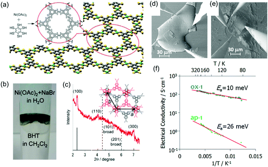 | ||
| Fig. 13 (a) Chemical structure of the monolayer HTB-Ni 2D c-MOF. (b) Synthesis of the 2D c-MOF film at the CH2Cl2–water interface. (c) XRD of the synthetic film. (d and e) SEM images for the van der Pauw measurement of oxidized and as-prepared HTB-Ni films, respectively. (f) Temperature dependent electrical conductivity. Sample thickness: 1 μm. Reproduced with permission from ref. 31 and 141. Copyright 2013 and 2014 American Chemical Society, respectively. | ||
By replacing the Ni centers with Cu centers, the Zhu group also synthesized free-standing, polycrystalline HTB-Cu 2D c-MOF films with thickness tailored from 20 to 200 nm at the CH2Cl2/H2O interface (Fig. 14a and b).142 An in-line four-probe conductivity measurement revealed a high conductivity of 1.58 × 10³ S cm−1 in a 150 nm-thick film at 300 K and the conductivity decreased upon cooling (Fig. 14c). However, analogous to the report from Nishihara et al.,141 the ultraviolet photoemission valence band spectrum and the band structure calculation elucidated its metallic feature. To further characterize the charge transport properties, a FET device was built with a bottom-gate, bottom-contact device geometry on a SiO2/Si substrate and 30 nm-thick gold patterns as the source and drain electrodes (Fig. 14d). The FET measurements showed an ambipolar charge transport behavior with high carrier mobilities (99 cm2 V−1 s−1 for holes and 116 cm2 V−1 s−1 for electrons) but a small on/off ratio (∼10). This behavior is typical for a FET fabricated from a gapless conductor. However, the observed mobility surpasses all previously reported organic ambipolar devices.
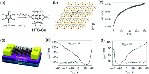 | ||
| Fig. 14 (a) Schematic synthesis of the HTB-Cu MOF. (b) Schematic structure of the 2D lattice of HTB-Cu with cell parameters of a = b = 8.76 Å. (c) Variable-temperature conductivity measurement on a 150 nm film by the in-line four-probe method. (d) Illustrative scheme of the HTB-Cu-based FET. (e and f) Output characteristics of the HTB-Cu-based FET. Reproduced with permission from ref. 142. Copyright 2015 Nature Publishing Group. | ||
The reports of the above materials reveal the potential of 2D c-MOFs as a new generation of electroactive layers, although the related performance is still limited for a logic electronic device. In 2015, Dincă et al. achieved the synthesis of a polycrystalline Ni3(HITP)2 2D c-MOF film with a thickness of ∼500 nm by placing a quartz substrate in the bulk solution (Fig. 15a).44 Although the obtained film was not homogeneous or smooth, it had a high conductivity of 40 S cm−1. The variable-temperature conductivity measurements suggested a semiconducting nature of the MOF film; the conductivity increased with the temperature. However, the corresponding semiconducting parameters including the charge carrier type, carrier mobility, and carrier concentration remained to be addressed. In 2017, Xu et al. employed an air–liquid interfacial growth method to prepare a high-quality, free-standing, polycrystalline Ni3(HITP)2 film with a smooth (RMS roughness of ∼1 nm) and dense surface (Fig. 15b).164 MOF films were initially transferred onto the solid substrates via a Langmuir–Schaefer transfer method. Next, a FET device was fabricated with a bottom-gate and top-contact device geometry based on a 105 nm-thick membrane as the active channel material, 50 nm thick Au thin films as the source and drain electrodes, and heavily doped p-type Si as the gate electrode. The transfer characteristics revealed a p-type depletion behavior, a typical threshold voltage of ∼1.1 V and a high carrier mobility of 48.6 cm2 V−1 s−1 (Fig. 15c and d). The device moreover displayed on/off current ratios as high as 2000. The observed mobility is competitive with state-of-the-art solution-processed organic and inorganic semiconductors, a remarkable feature for a material that consists in a significant part of empty pore space. The authors pointed out that no saturation current was observed and that the device showed gapless conductor behavior.
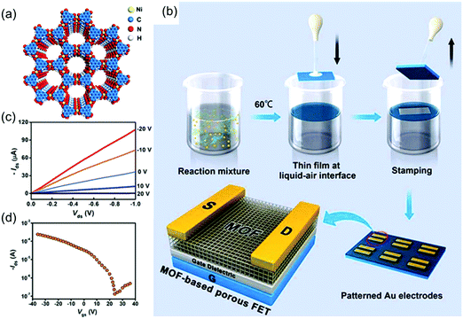 | ||
| Fig. 15 (a) Schematic structure of semiconducting Ni3(HITP)2. (b) Schematic illustration of the fabrication of Ni3(HITP)2 film-based porous FETs. (c and d) Output curves and transfer curve for the Ni3(HITP)2-based FET, respectively. Reproduced with permission from ref. 164. Copyright 2017 American Chemical Society. | ||
4. Bringing 2DCPs toward memory devices
A memristor is a hypothetical non-linear passive two-terminal electrical component relating electric charge and magnetic flux linkage.165–170 It was envisioned by circuit theorist Leon Chua in 1971165 and was linked to physical devices with a metal–insulator–metal architecture by HP Labs in 2008.167 It displays bipolar switching of resistance through field-dependent hysteresis. The current–voltage behavior of the element can be switched between a high and low resistance state by opposite writing and erasing voltage sweeps, i.e. storing digital ON and OFF signals.171 Importantly, in order to be interesting for low-power applications, switching needs to occur at a relatively low threshold voltage. Switching in memory resistors can either be based on physical processes, such as phase transitions, charge trapping, ferroelectrics or magnetics, or on chemical processes, typically involving the reversible formation of mobile ion gradients or passivation layers. Although relatively new circuit elements, memristors based on ceramics are promising for integration in data storage in the form of resistive random access memory (RRAM).Covalent bonds are a class of very stable chemical bonds that enable these materials to exhibit high stability in many solvents and high-temperature environments. At present, large-area monolayer 2D COF films have been successfully prepared. Their ultrathinness is expected to reduce the filament length to the atomic scale, which not only facilitates miniaturization of the memristor but also helps minimize the need for energy to form and rupture the conductive filaments. More strikingly, 2D COFs are intrinsically porous and the structure and the pore environment can be intentionally engineered through monomer design and post synthetic modification. This has yielded promising applications requiring ion conduction,75,76,172–174 which is also a key consideration when selecting memristive materials. Therefore, these unique characteristics of 2D COFs are highly desirable in the field of memristors. However, to date there are rather limited reports on the use of 2D COFs for the preparation of memristive devices.
Recently, Hu, Lei and co-workers synthesized a wafer-scale 2D COF film (named 2DPBTA+PDA, shown in Fig. 16a) with tunable thickness at the air–liquid interface via the condensation between benzene-1,3,5-tricarbaldehyde (BTA) and p-phenylenediamine (PDA).175Fig. 16b presents an as-grown ultrathin 2D COF film with a thickness of 1.8 ± 0.2 nm and good freestanding ability. The intrinsic porosity, the coordination ability of the imine groups, and the high uniformity of this 2DPBTA+PDA film make it a desired resistive switching medium layer in electrochemical metallization (ECM) memories. Memristors based on these ultrathin 2D COF films (Ag/2DPBTA+PDA/ITO) exhibited nonvolatile bipolar resistive switching behavior with high reliability and reproducibility, with on/off ratios in the range of 102 to 105 depending on the thickness of the film (Fig. 16c and d). Furthermore, the typical two-terminal device had high thermal stability with an operating temperature of up to 400 °C, together with good resistance to many organic solvents. Finally, the intrinsic flexibility of this film enabled its application in flexible devices (Fig. 16e), in which it displayed as reliable performance as that on a rigid substrate.
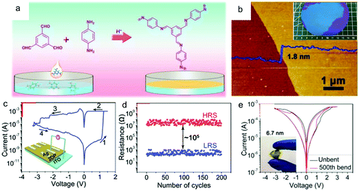 | ||
| Fig. 16 (a) A schematic illustration of the synthesis of 2DPBTA+PDA films through the Schiff-base reaction of the monomers. (b) AFM image of a 1.8 ± 0.2 nm thick 2DPBTA+PDA film on a silicon wafer. (c) I–V plots for the initial formation process (inset: the schematic diagram of the resistive switching device with a Ag/2DPBTA+PDA/ITO configuration). (d) Endurance performance of the on/off resistances plotted as a function of the number of cycles. (e) Switching curves of a flexible Ag/2DPBTA+PDA/graphene device before and after repeated mechanical bending of up to 500 cycles (inset: a photograph of the flexible device under bending). Reproduced with permission from ref. 175. Copyright 2019 Wiley & Sons. | ||
In our newest results, we employed the SMAIS method to prepare boronate ester 2D COFs with different pore sizes by varying the building blocks (Fig. 17a).37 As mentioned above, the achieved 2D COFs are free-standing thin films with large single-crystalline domains up to ∼60 μm2 and tunable thickness from 6 to 16 nm. The molecular-level structures were ambiguously resolved by HR-TEM imaging (Fig. 17b) and SAED measurements. Due to the high crystallinity, facile thin-film processability, and high mechanical stability as well as the incorporation of electroactive porphyrin monomers, a hybrid memory device was fabricated by transferring the 2D COF film from the water surface onto a silicon nanowire-based field-effect transistor, as shown in Fig. 17c. Substantial hysteresis, giving information about the charge trapping and storage capability of the device, was observed for the hybrid devices. The threshold voltage was higher in the up-sweep (red arrow in Fig. 17d) stage than in the down sweep (black arrow in Fig. 17d) stage, suggesting the positive polarity of the trapped charges in the device, while the threshold voltage of the bare device was constant. This hysteresis behavior is compulsory for memory effects to mimic neuronal synapses with a fast response of 20 s for the saturation of the potentiation (Fig. 17e), including potentiation (learning), depression (erasing) and relaxation (forgetting) processes. A pulsed voltage input induces the polarization of the film, which is critical to emulate the potentiation of the neuronal membrane. This work paved the way to develop highly crystalline 2D COF thin films as an easy-to-fabricate active component applicable for CMOS-compatible neuromorphic computing. Inspired by these results, a new research field for the production of flexible 2D COF-based memory devices will be rising, which will allow high-temperature resistance and high robustness to satisfy future demands in wearable devices.
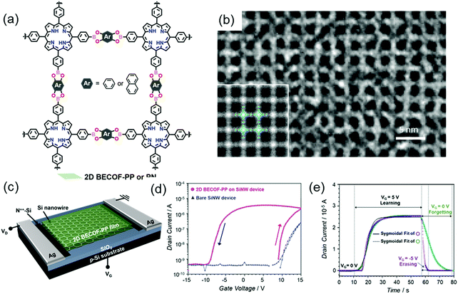 | ||
| Fig. 17 (a) Chemical structure of the boronate ester-based 2D COFs. (b) HR-TEM image. The inset is a lattice-averaged image calculated from DFT. (c) Schematics of the 2D COF/SiNW hybrid device. (d) Transfer characteristics of the hybrid device. (e) Learn–erase/learn–forget cycles. Reproduced with permission from ref. 37. Copyright 2020 Wiley & Sons. | ||
5. Bringing 2DCPs toward photodetectors
As is shown, the reported 2D c-MOFs display exciting electrical conductivity and potential for logic electronic circuits, but the nature of the charge transport has remained ambiguous mainly due to the current synthetic issues. Very recently, to disclose the nature of charge transport in 2D c-MOFs, we reported a study of MOF conductivity using time-resolved terahertz spectroscopy (TRTS),132 an all-optical, contact-free method capable of addressing the nature of charge transport. TRTS provides high-frequency (0.6–1.6 THz) complex photoconductivity, which directly reflects the mechanism of charge transport.176 We synthesized a large-area free-standing multilayer triphenylenehexathiol-Fe (Fe3(THT)2) 2D c-MOF film by an interfacial method in which aqueous and CHCl3 phases hosted THT and iron precursors, respectively (Fig. 18a). The film thickness was tunable by the reaction time (from 20 nm to ∼2 μm after 72 reaction hours). DFT calculation of the electronic structures revealed a semiconducting behavior with a band gap of ∼350 meV. The achieved porous thin films of Fe3(THT)2 supported band-like charge carrier transport, directly demonstrated from the observed Drude-type complex photoconductivity. A room temperature mobility of ∼220 cm2 V−1 s−1 was estimated from TRTS (Fig. 18b), which represented a record mobility in the reported MOFs. Notably, this mobility value was independently verified using Hall effect measurements based on a Hall bar structure of the Fe3(THT)2 film (inset image in Fig. 18c). The Hall geometry of the MOF layer on a Si/SiO2 (300 nm) wafer was fabricated using cold ablation via ultrafast laser pulses. After that, a 5 nm-thick Cr layer and a 150 nm-thick Au layer were deposited as the metallic contacts by electron beam lithography. The Hall effects were investigated with temperature from 100 K to RT and a vertical magnetic field that reached ±2.5 T. The quantitative agreement between the inferred THz and Hall mobilities demonstrated that band-like charge carrier transport was operative in the samples in both the a.c. and d.c. limit. The analysis of the temperature dependence of the conductivity from both methods revealed that the scattering rates and hence mobilities are primarily limited by impurity scattering so that the inferred mobilities constitute lower limits (Fig. 18b). Thermally excited carriers were responsible for the temperature dependence of the four-probe conductivity, as opposed to a reduction in the DC mobility of the carriers (Fig. 18c).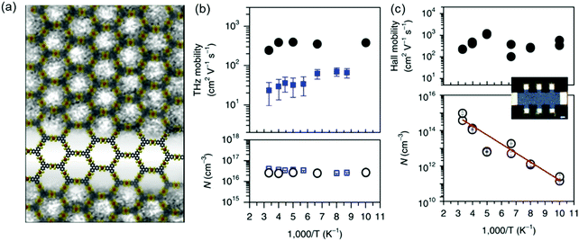 | ||
| Fig. 18 (a) A high-resolution transmission electron microscopy image of the Fe3(THT)2 2D conjugated MOF together with the structural schematic (grey, yellow and orange: carbon, sulfur and iron atoms, respectively). (b and c) Charge transport studies by THz spectroscopy and Hall effect measurements, respectively. Scale bar: 100 μm. Reproduced with permission from ref. 132. Copyright 2018 Nature Publishing Group. | ||
These above results illustrated the potential for high-mobility semiconducting MOFs as active materials in thin film optoelectronic devices. In our newest results, we demonstrated the ability of free-standing 2D c-MOF films of Fe3(THT)2 to serve as an active element in a two-terminal photodetector device (Fig. 19a).177 Changes in device conductance were revealed upon light exposure ranging from UV to NIR wavelengths (400–1575 nm). Temperature-dependent photocurrent measurements demonstrated that the photodetector showed a stronger photoresponse and higher sensitivity at liquid nitrogen temperatures (77 K) than at room temperature (Fig. 19b). In addition, a drastic improvement in the photodetector's figures of merit, such as photosensitivity (defined as the ratio of photocurrent to dark current), voltage responsivity (Rv), noise equivalent power (NEP) and specific detectivity (D*), was achieved on cooling the devices to 77 K. These results were consistent with the low IR bandgap of the samples, which caused strong thermally activated band-to-band population of free charge carriers at room temperature, described by N ∝ exp[−Eg/2kT]. Cooling the devices suppressed this thermal generation of charge carriers, which consequently led to much improved device performance. Furthermore, the devices showed stable and reproducible photoswitching behavior as a function of time. From Fig. 19b, the rise and decay times at 77 K are found to be 2.3 s and 2.15 s, respectively, an increase from ∼1.7 s for both at 300 K. On testing multiple samples, response times in the range of 1–3 s were obtained. These response times were affected severely by the types and density of defects in the material, and thus could be shortened further by defect engineering to achieve a faster response. Such a broadband photoresponse was reported for the first time for an entirely 2D c-MOF-based photodetector and demonstrated a reliable and robust device.
 | ||
| Fig. 19 (a) Schematic of a two-terminal photodetector device based on a 1.7 μm thick MOF layer with indium electrodes. (b) Photoswitching behavior under pulsed illumination of a 785 nm laser. Temperature-dependent photoresponse as a function of time at P = 0.14 W cm−2 and V = −1 V. The device shows long-term stable photoswitching capability. (c) Time-resolved response zoomed for 77 K showing a response time of ≈2 s. Reproduced with permission from ref. 177. Copyright 2020 Wiley & Sons. | ||
6. Summary and outlook
In this current review article, we highlight the liquid-interface-assisted synthesis (LIAS) methods, such as LB-assisted synthesis, liquid–liquid interfacial synthesis and SMAIS, for the preparation of single- or multi-layer 2DCP films. The LIAS strategy allows the mobility and exchange of the monomers and guides their pre-organization into layers in a 2D confined space. In this respect, directional 2D polymerization like polycondensation, polycoupling and coordination reactions can be applied successfully to provide well-defined 2DCP films, such as graphdiyne, 2D polymers, 2D c-COF films and 2D c-MOF films. Fine-tuned thickness and lateral size as well as structural diversity at the molecular level have been realized. Benefiting from the π-conjugated structures, intrinsic conductivity and tunable band gaps as well as thin films and facile processing, the developed 2DCPs have been rising as a new generation of organic electrode materials for broad applications in FETs, memristors and photodetectors.For this moment, it is important to clarify that traditional semiconductors should not be the metric by which 2DCPs should be regarded as photo-/electro-active materials. One can ask whether 2DCPs can even outperform these traditional electronic materials. This question cannot be fully addressed without specifying the particular property, function, and device type. If compared with silicon, the answer is likely to be no. For example, the intrinsic electron and hole mobilities for crystalline silicon at 300 K are 1450–1610 cm2 V−1 s−1 and 300–400 cm2 V−1 s−1, respectively (Hall effect); whereas the thus-far reported highest values for 2DCPs are 116 cm2 V−1 s−1 (HTB-Cu MOF, electrons, FET)142 and ∼220 cm2 V−1 s−1 (Fe3(THT)2 MOF, holes, Hall).132 Regardless of whether 2DCP properties become better than traditional materials, they will likely never displace silicon-based inorganic semiconductors. However, the reported mobilities for 2DCPs considerably exceed those of typical crystalline organic semiconductors, which now are mostly in the 1–20 cm2 V−1 s−1 range (a few examples could reach up to ∼30 cm2 V−1 s−1).1–8 It is apparent that 2DCPs should be considered as a unique class of electronic materials that exhibit unique properties, i.e., porosity, crystallinity, highly tailorable structure, and tunable thickness from a single layer to a few layers. For example, the ability to tailor the electrical conductivity of 2DCPs without resorting to doping is far greater than for silicon. Similarly, 2DCP bandgaps exhibit a range of values comparable to amorphous organic molecule/polymer films. Owing to their crystalline structure, bandgap tuning is possible to a greater extent than in disordered materials. In addition, for semiconductive organic molecule/polymer single crystals, it is quite complicated to ultrathin the crystals into single or few layers, whereas free-standing 2DCP films represent a kind of advantage in processing and device integration.
Despite the recent success, many critical issues related to controlled synthesis and devices remain to be addressed.
(i) The LIAS strategy is advantageous for the synthesis of large-area, free-standing 2DCP films with varied thickness. However, the issues concerning structural perfection such as homogeneous crystalline phases, large grain size, minimized amorphous regions, engineered grain boundaries and edge structures of synthetic 2DCPs have not been addressed so far. Particularly, a single-crystalline single-layer 2DCP film has not been achieved. Those features can significantly influence the physical and chemical properties of 2DCPs. Very recently, a mesoscale ordered 2DCP, with domain dimensions greater than 100 nm, by Ullmann coupling of rigid, achiral heterotriangulene precursors on the Au(111) surface was reported.178 The mesoscale size of the network enabled the characterization of the occupied band structure by angle-resolved photoelectron spectroscopy (ARPES) with a synchrotron source, which revealed Dirac cones at the K point in the valence band and flat bands below the Fermi level. Thus, a higher-level controlled synthesis is crucial, which highly depends on the design of the precursors, such as the solubility, chemical stability, reactivity and desired interactions with interfaces. Moreover, chemical methodologies for 2D polymerization require development to eliminate amorphousness and defects of 2DCPs and improve the conjugation length.
(ii) Fundamental understanding of LIAS is still in its infancy. Interfacial synthesis has exhibited enormous advantages to enhance the ordering of monomers and lower the reaction barriers. However, the mechanism behind it is still elusive, especially at the molecular/atomic level. Correspondingly, multi-scale characterization methods and in situ probing strategies shall be employed towards studies of the interfacial reaction mechanism. In addition, the characterization of local structure and the quantification of the defect content as well as the understanding of defect formation at the atomic level are still in their infancy, not to mention their potential influences on the material functionalities.
(iii) The pre-organization of monomers is a critical step which can control the topology and crystallinity of 2DCPs synthesized at interfaces. In this respect, a surfactant monolayer has been demonstrated to provide the opportunity for fine control of the monomer assembly and then contribute to controlled 2D polymerization with long-range ordering. However, many open fundamental questions have to be addressed, such as the “true” role of the surfactant monolayer, the design and selectivity of surfactants, the reaction kinetics and thermodynamics affected by the surfactants, layer number control and the development of polymerization methodologies.
(iv) The transfer processing of these 2DCP films from interfaces should also be improved due to possible structural distortion and folding and tearing of the sheets, and possible oxidation of some air-sensitive 2DCPs in ambient conditions leading to structural decomposition and impurity contamination from the solvents, which heavily dope the 2DCPs. These issues are highly related to the further development of LIAS strategies and processing technologies.
(V) Finally, even demonstrated to exhibit promising performance, the applications of 2DCPs in organic electronics are still rather preliminary. One can expect that the structural diversity, intrinsic optical, electronic and magnetic properties and catalytic reactivity of 2DCPs will bring them into novel logic and memory devices, such as OLEDs, OFETs, OPVs, ORFIDs and organic spintronics. Nevertheless, the unprecedented properties highly rely on structural control of 2DCPs at the atomic and molecular level. Thus, a reliable and fundamental structure–property relationship should be addressed firstly, which will push the development of 2DCPs via LIAS in the future.
Conflicts of interest
There are no conflicts to declare.Acknowledgements
This work is financially supported by EU Graphene Flagship (No. 785219), ERC starting grant (FC2DMOF, No. 852909), DFG project (Chemistry of Synthetic Two-Dimensional Materials, CRC 1415, No. 417590517), Coordination Networks: Building Blocks for Functional Systems (SPP 1928, COORNET), and the German Science Council and Center of Advancing Electronics Dresden (cfaed). Renhao appreciates the helpful discussion with Prof. Xinliang Feng (TU Dresden).References
- G. Yu, J. Gao, J. C. Hummelen, F. Wudl and A. J. Heeger, Science, 1995, 270, 1789–1791 CrossRef CAS.
- H. Sirringhaus, N. Tessler and R. H. Friend, Science, 1998, 280, 1741–1744 CrossRef CAS.
- A. J. Heeger, Chem. Soc. Rev., 2010, 39, 2354–2371 RSC.
- A. Facchetti, Chem. Mater., 2011, 23, 733–758 CrossRef CAS.
- C. Wang, H. Dong, W. Hu, Y. Liu and D. Zhu, Chem. Rev., 2012, 112, 2208–2267 CrossRef CAS.
- X. Guo, M. Baumgarten and K. Müllen, Prog. Polym. Sci., 2013, 38, 1832–1908 CrossRef CAS.
- S. Fratini, M. Nikolka, A. Salleo, G. Schweicher and H. Sirringhaus, Nat. Mater., 2020, 19, 491–502 CrossRef CAS.
- F. Yang, S. Cheng, X. Zhang, X. Ren, R. Li, H. Dong and W. Hu, Adv. Mater., 2018, 30, 1702415 CrossRef.
- R. Dong, T. Zhang and X. Feng, Chem. Rev., 2018, 118, 6189–6235 CrossRef CAS.
- L. Wang, H. Sahabudeen, T. Zhang and R. Dong, npj 2D Mater. Appl., 2018, 2, 26 CrossRef.
- R. H. Baughman, H. Eckhardt and M. Kertesz, J. Chem. Phys., 1987, 87, 6687–6699 CrossRef CAS.
- N. Narita, S. Nagai, S. Suzuki and K. Nakao, Phys. Rev. B: Condens. Matter Mater. Phys., 1998, 58, 11009–11014 CrossRef CAS.
- K. Tanaka, N. Kosai, H. Maruyama and H. Kobayashi, Synth. Met., 1998, 92, 253–258 CrossRef CAS.
- R. Gutzler and D. F. Perepichka, J. Am. Chem. Soc., 2013, 135, 16585–16594 CrossRef CAS.
- K. S. Novoselov, A. K. Geim, S. V. Morozov, D. Jiang, Y. Zhang, S. V. Dubonos, I. V. Grigorieva and A. A. Firsov, Science, 2004, 306, 666–669 CrossRef CAS.
- A. K. Geim, Science, 2009, 324, 1530–1534 CrossRef CAS.
- K. Müllen, Nat. Rev. Mater., 2016, 1, 15013 CrossRef.
- L. Grill, M. Dyer, L. Lafferentz, M. Persson, M. V. Peters and S. Hecht, Nat. Nanotechnol., 2007, 2, 687–691 CrossRef CAS.
- M. Bieri, M. Treier, J. Cai, K. Aït-Mansour, P. Ruffieux, O. Gröning, P. Gröning, M. Kastler, R. Rieger, X. Feng, K. Müllen and R. Fasel, Chem. Commun., 2009, 6919–6921 RSC.
- J. F. Dienstmaier, D. D. Medina, M. Dogru, P. Knochel, T. Bein, W. M. Heckl and M. Lackinger, ACS Nano, 2012, 6, 7234–7242 CrossRef CAS.
- L. Lafferentz, V. Eberhardt, C. Dri, C. Africh, G. Comelli, F. Esch, S. Hecht and L. Grill, Nat. Chem., 2012, 4, 215–220 CrossRef CAS.
- L. Cardenas, R. Gutzler, J. Lipton-Duffin, C. Fu, J. L. Brusso, L. E. Dinca, M. Vondráček, Y. Fagot-Revurat, D. Malterre, F. Rosei and D. F. Perepichka, Chem. Sci., 2013, 4, 3263–3268 RSC.
- X.-H. Liu, C.-Z. Guan, S.-Y. Ding, W. Wang, H.-J. Yan, D. Wang and L.-J. Wan, J. Am. Chem. Soc., 2013, 135, 10470–10474 CrossRef CAS.
- P. Kissel, R. Erni, W. B. Schweizer, M. D. Rossell, B. T. King, T. Bauer, S. Götzinger, A. D. Schlüter and J. Sakamoto, Nat. Chem., 2012, 4, 287–291 CrossRef CAS.
- Y. Peng, Y. Li, Y. Ban, H. Jin, W. Jiao, X. Liu and W. Yang, Science, 2014, 346, 1356–1359 CrossRef CAS.
- W. Liu, X. Luo, Y. Bao, Y. P. Liu, G.-H. Ning, I. Abdelwahab, L. Li, C. T. Nai, Z. G. Hu, D. Zhao, B. Liu, S. Y. Quek and K. P. Loh, Nat. Chem., 2017, 9, 563–570 CrossRef CAS.
- M. A. Khayum, S. Kandambeth, S. Mitra, S. B. Nair, A. Das, S. S. Nagane, R. Mukherjee and R. Banerjee, Angew. Chem., Int. Ed., 2016, 55, 15604–15608 CrossRef CAS.
- D. N. Bunck and W. R. Dichtel, J. Am. Chem. Soc., 2013, 135, 14952–14955 CrossRef CAS.
- R. Makiura, S. Motoyama, Y. Umemura, H. Yamanaka, O. Sakata and H. Kitagawa, Nat. Mater., 2010, 9, 565–571 CrossRef CAS.
- T. Bauer, Z. Zheng, A. Renn, R. Enning, A. Stemmer, J. Sakamoto and A. D. Schlüter, Angew. Chem., Int. Ed., 2011, 50, 7879–7884 CrossRef CAS.
- T. Kambe, R. Sakamoto, K. Hoshiko, K. Takada, M. Miyachi, J.-H. Ryu, S. Sasaki, J. Kim, K. Nakazato, M. Takata and H. Nishihara, J. Am. Chem. Soc., 2013, 135, 2462–2465 CrossRef CAS.
- R. Dong, M. Pfeffermann, H. Liang, Z. Zheng, X. Zhu, J. Zhang and X. Feng, Angew. Chem., Int. Ed., 2015, 54, 12058–12063 CrossRef CAS.
- D. Sheberla, J. C. Bachman, J. S. Elias, C.-J. Sun, Y. Shao-Horn and M. Dincă, Nat. Mater., 2016, 16, 220 CrossRef.
- H. Sahabudeen, H. Qi, B. A. Glatz, D. Tranca, R. Dong, Y. Hou, T. Zhang, C. Kuttner, T. Lehnert, G. Seifert, U. Kaiser, A. Fery, Z. Zheng and X. Feng, Nat. Commun., 2016, 7, 13461 CrossRef CAS.
- K. Liu, H. Qi, R. Dong, R. Shivhare, M. Addicoat, T. Zhang, H. Sahabudeen, T. Heine, S. Mannsfeld, U. Kaiser, Z. Zheng and X. Feng, Nat. Chem., 2019, 11, 994–1000 CrossRef CAS.
- T. Zhang, H. Qi, Z. Liao, Y. D. Horev, L. A. Panes-Ruiz, P. S. Petkov, Z. Zhang, R. Shivhare, P. Zhang, K. Liu, V. Bezugly, S. Liu, Z. Zheng, S. Mannsfeld, T. Heine, G. Cuniberti, H. Haick, E. Zschech, U. Kaiser, R. Dong and X. Feng, Nat. Commun., 2019, 10, 4225 CrossRef.
- S. Park, Z. Liao, B. Ibarlucea, H. Qi, H.-H. Lin, D. Becker, J. Melidonie, T. Zhang, H. Sahabudeen, L. Baraban, C.-K. Baek, Z. Zheng, E. Zschech, A. Fery, T. Heine, U. Kaiser, G. Cuniberti, R. Dong and X. Feng, Angew. Chem., Int. Ed., 2020, 59, 8218–8224 CrossRef CAS.
- H. Sahabudeen, H. Qi, M. Ballabio, M. Položij, S. Olthof, R. Shivhare, Y. Jing, S. Park, K. Liu, T. Zhang, J. Ma, B. Rellinghaus, S. Mannsfeld, T. Heine, M. Bonn, E. Cánovas, Z. Zheng, U. Kaiser, R. Dong and X. Feng, Angew. Chem., Int. Ed., 2020, 59, 6028–6036 CrossRef CAS.
- G. Li, Y. Li, H. Liu, Y. Guo, Y. Li and D. Zhu, Chem. Commun., 2010, 46, 3256–3258 RSC.
- Y. Li, L. Xu, H. Liu and Y. Li, Chem. Soc. Rev., 2014, 43, 2572–2586 RSC.
- J. W. Colson and W. R. Dichtel, Nat. Chem., 2013, 5, 453–465 CrossRef CAS.
- X. Feng and A. D. Schlüter, Angew. Chem., Int. Ed., 2018, 57, 13748–13763 CrossRef CAS.
- C. S. Diercks and O. M. Yaghi, Science, 2017, 355, eaal1585 CrossRef.
- D. Sheberla, L. Sun, M. A. Blood-Forsythe, S. Er, C. R. Wade, C. K. Brozek, A. Aspuru-Guzik and M. Dincă, J. Am. Chem. Soc., 2014, 136, 8859–8862 CrossRef CAS.
- N. Huang, P. Wang and D. Jiang, Nat. Rev. Mater., 2016, 1, 16068 CrossRef CAS.
- M. S. Lohse and T. Bein, Adv. Funct. Mater., 2018, 28, 1705553 CrossRef.
- H. Wang, Z. Zeng, P. Xu, L. Li, G. Zeng, R. Xiao, Z. Tang, D. Huang, L. Tang, C. Lai, D. Jiang, Y. Liu, H. Yi, L. Qin, S. Ye, X. Ren and W. Tang, Chem. Soc. Rev., 2019, 48, 488–516 RSC.
- M. Zhao, Y. Huang, Y. Peng, Z. Huang, Q. Ma and H. Zhang, Chem. Soc. Rev., 2018, 47, 6267–6295 RSC.
- Y. A. Mezenov, A. A. Krasilin, V. P. Dzyuba, A. Nominé and V. A. Milichko, Adv. Sci., 2019, 6, 1900506 CrossRef.
- M. Ko, L. Mendecki and K. A. Mirica, Chem. Commun., 2018, 54, 7873–7891 RSC.
- L. Sun, M. G. Campbell and M. Dincă, Angew. Chem., Int. Ed., 2016, 55, 3566–3579 CrossRef CAS.
- J. T. Culp, J.-H. Park, D. Stratakis, M. W. Meisel and D. R. Talham, J. Am. Chem. Soc., 2002, 124, 10083–10090 CrossRef CAS.
- P. Payamyar, K. Kaja, C. Ruiz-Vargas, A. Stemmer, D. J. Murray, C. J. Johnson, B. T. King, F. Schiffmann, J. VandeVondele, A. Renn, S. Götzinger, P. Ceroni, A. Schütz, L.-T. Lee, Z. Zheng, J. Sakamoto and A. D. Schlüter, Adv. Mater., 2014, 26, 2052–2058 CrossRef CAS.
- D. J. Murray, D. D. Patterson, P. Payamyar, R. Bhola, W. Song, M. Lackinger, A. D. Schlüter and B. T. King, J. Am. Chem. Soc., 2015, 137, 3450–3453 CrossRef CAS.
- M. E. Belowich and J. F. Stoddart, Chem. Soc. Rev., 2012, 41, 2003–2024 RSC.
- X. Feng, X. Ding and D. Jiang, Chem. Soc. Rev., 2012, 41, 6010–6022 RSC.
- J. L. Segura, M. J. Mancheño and F. Zamora, Chem. Soc. Rev., 2016, 45, 5635–5671 RSC.
- W. Dai, F. Shao, J. Szczerbiński, R. McCaffrey, R. Zenobi, Y. Jin, A. D. Schlüter and W. Zhang, Angew. Chem., Int. Ed., 2016, 55, 213–217 CrossRef CAS.
- R. Matsuoka, R. Sakamoto, K. Hoshiko, S. Sasaki, H. Masunaga, K. Nagashio and H. Nishihara, J. Am. Chem. Soc., 2017, 139, 3145–3152 CrossRef CAS.
- K. Dey, M. Pal, K. C. Rout, S. H. Kunjattu, A. Das, R. Mukherjee, U. K. Kharul and R. Banerjee, J. Am. Chem. Soc., 2017, 139, 13083–13091 CrossRef CAS.
- M. Matsumoto, L. Valentino, G. M. Stiehl, H. B. Balch, A. R. Corcos, F. Wang, D. C. Ralph, B. J. Mariñas and W. R. Dichtel, Chemistry, 2018, 4, 308–317 CrossRef CAS.
- S. Mitra, S. Kandambeth, B. P. Biswal, A. M. Khayum, C. K. Choudhury, M. Mehta, G. Kaur, S. Banerjee, A. Prabhune, S. Verma, S. Roy, U. K. Kharul and R. Banerjee, J. Am. Chem. Soc., 2016, 138, 2823–2828 CrossRef CAS.
- Y. Zhong, B. Cheng, C. Park, A. Ray, S. Brown, F. Mujid, J.-U. Lee, H. Zhou, J. Suh, K.-H. Lee, A. J. Mannix, K. Kang, S. J. Sibener, D. A. Muller and J. Park, Science, 2019, 366, 1379–1384 CrossRef CAS.
- R. Dong and J. Hao, Chem. Rev., 2010, 110, 4978–5022 CrossRef CAS.
- A. P. Côté, A. I. Benin, N. W. Ockwig, M. O'Keeffe, A. J. Matzger and O. M. Yaghi, Science, 2005, 310, 1166–1170 CrossRef.
- H. Furukawa and O. M. Yaghi, J. Am. Chem. Soc., 2009, 131, 8875–8883 CrossRef CAS.
- Y. Zeng, R. Zou and Y. Zhao, Adv. Mater., 2016, 28, 2855–2873 CrossRef CAS.
- C. Zhang, B.-H. Wu, M.-Q. Ma, Z. Wang and Z.-K. Xu, Chem. Soc. Rev., 2019, 48, 3811–3841 RSC.
- V. A. Kuehl, J. Yin, P. H. H. Duong, B. Mastorovich, B. Newell, K. D. Li-Oakey, B. A. Parkinson and J. O. Hoberg, J. Am. Chem. Soc., 2018, 140, 18200–18207 CrossRef CAS.
- S.-Y. Ding, J. Gao, Q. Wang, Y. Zhang, W.-G. Song, C.-Y. Su and W. Wang, J. Am. Chem. Soc., 2011, 133, 19816–19822 CrossRef CAS.
- H. Xu, J. Gao and D. Jiang, Nat. Chem., 2015, 7, 905 CrossRef CAS.
- X. Han, Q. Xia, J. Huang, Y. Liu, C. Tan and Y. Cui, J. Am. Chem. Soc., 2017, 139, 8693–8697 CrossRef CAS.
- Z. Li, N. Huang, K. H. Lee, Y. Feng, S. Tao, Q. Jiang, Y. Nagao, S. Irle and D. Jiang, J. Am. Chem. Soc., 2018, 140, 12374–12377 CrossRef CAS.
- Z. Meng, R. M. Stolz and K. A. Mirica, J. Am. Chem. Soc., 2019, 141, 11929–11937 CrossRef CAS.
- Z. Xie, B. Wang, Z. Yang, X. Yang, X. Yu, G. Xing, Y. Zhang and L. Chen, Angew. Chem., Int. Ed., 2019, 58, 15742–15746 CrossRef CAS.
- H. S. Sasmal, H. B. Aiyappa, S. N. Bhange, S. Karak, A. Halder, S. Kurungot and R. Banerjee, Angew. Chem., Int. Ed., 2018, 57, 10894–10898 CrossRef CAS.
- H. Xu, S. Tao and D. Jiang, Nat. Mater., 2016, 15, 722 CrossRef CAS.
- B. P. Biswal, S. Valligatla, M. Wang, T. Banerjee, N. A. Saad, B. M. K. Mariserla, N. Chandrasekhar, D. Becker, M. Addicoat, I. Senkovska, R. Berger, D. N. Rao, S. Kaskel and X. Feng, Angew. Chem., Int. Ed., 2019, 58, 6896–6900 CrossRef CAS.
- H. Phan, T. S. Herng, D. Wang, X. Li, W. Zeng, J. Ding, K. P. Loh, A. T. Shen Wee and J. Wu, Chemistry, 2019, 5, 1223–1234 CrossRef CAS.
- Y. Jiang, I. Oh, S. H. Joo, O. Buyukcakir, X. Chen, S. H. Lee, M. Huang, W. K. Seong, J. H. Kim, J.-U. Rohde, S. K. Kwak, J.-W. Yoo and R. S. Ruoff, ACS Nano, 2019, 13, 5251–5258 CrossRef CAS.
- S. Wu, M. Li, H. Phan, D. Wang, T. S. Herng, J. Ding, Z. Lu and J. Wu, Angew. Chem., Int. Ed., 2018, 57, 8007–8011 CrossRef CAS.
- E. Jin, M. Asada, Q. Xu, S. Dalapati, M. A. Addicoat, M. A. Brady, H. Xu, T. Nakamura, T. Heine, Q. Chen and D. Jiang, Science, 2017, 357, 673–676 CrossRef CAS.
- T. Sick, A. G. Hufnagel, J. Kampmann, I. Kondofersky, M. Calik, J. M. Rotter, A. Evans, M. Döblinger, S. Herbert, K. Peters, D. Böhm, P. Knochel, D. D. Medina, D. Fattakhova-Rohlfing and T. Bein, J. Am. Chem. Soc., 2018, 140, 2085–2092 CrossRef CAS.
- G. Wang, N. Chandrasekhar, B. P. Biswal, D. Becker, S. Paasch, E. Brunner, M. Addicoat, M. Yu, R. Berger and X. Feng, Adv. Mater., 2019, 31, 1901478 CrossRef.
- S. Xu, G. Wang, B. P. Biswal, M. Addicoat, S. Paasch, W. Sheng, X. Zhuang, E. Brunner, T. Heine, R. Berger and X. Feng, Angew. Chem., Int. Ed., 2019, 58, 849–853 CrossRef CAS.
- W. Liu, M. Ulaganathan, I. Abdelwahab, X. Luo, Z. Chen, S. J. Rong Tan, X. Wang, Y. Liu, D. Geng, Y. Bao, J. Chen and K. P. Loh, ACS Nano, 2018, 12, 852–860 CrossRef CAS.
- H. Duan, P. Lyu, J. Liu, Y. Zhao and Y. Xu, ACS Nano, 2019, 13, 2473–2480 CAS.
- X. Chen, Y. Li, L. Wang, Y. Xu, A. Nie, Q. Li, F. Wu, W. Sun, X. Zhang, R. Vajtai, P. M. Ajayan, L. Chen and Y. Wang, Adv. Mater., 2019, 31, 1901640 CrossRef.
- S. Wang, Q. Wang, P. Shao, Y. Han, X. Gao, L. Ma, S. Yuan, X. Ma, J. Zhou, X. Feng and B. Wang, J. Am. Chem. Soc., 2017, 139, 4258–4261 CrossRef CAS.
- S. Wan, J. Guo, J. Kim, H. Ihee and D. Jiang, Angew. Chem., Int. Ed., 2008, 47, 8826–8830 CrossRef CAS.
- M. Martínez-Abadía, C. T. Stoppiello, K. Strutynski, B. Lerma-Berlanga, C. Martí-Gastaldo, A. Saeki, M. Melle-Franco, A. N. Khlobystov and A. Mateo-Alonso, J. Am. Chem. Soc., 2019, 141, 14403–14410 CrossRef.
- E. L. Spitler and W. R. Dichtel, Nat. Chem., 2010, 2, 672–677 CrossRef CAS.
- S. Wan, F. Gándara, A. Asano, H. Furukawa, A. Saeki, S. K. Dey, L. Liao, M. W. Ambrogio, Y. Y. Botros, X. Duan, S. Seki, J. F. Stoddart and O. M. Yaghi, Chem. Mater., 2011, 23, 4094–4097 CrossRef CAS.
- M. Calik, F. Auras, L. M. Salonen, K. Bader, I. Grill, M. Handloser, D. D. Medina, M. Dogru, F. Löbermann, D. Trauner, A. Hartschuh and T. Bein, J. Am. Chem. Soc., 2014, 136, 17802–17807 CrossRef CAS.
- S. Dalapati, M. Addicoat, S. Jin, T. Sakurai, J. Gao, H. Xu, S. Irle, S. Seki and D. Jiang, Nat. Commun., 2015, 6, 7786 CrossRef CAS.
- J. I. Feldblyum, C. H. McCreery, S. C. Andrews, T. Kurosawa, E. J. G. Santos, V. Duong, L. Fang, A. L. Ayzner and Z. Bao, Chem. Commun., 2015, 51, 13894–13897 RSC.
- X. Zhuang, W. Zhao, F. Zhang, Y. Cao, F. Liu, S. Bi and X. Feng, Polym. Chem., 2016, 7, 4176–4181 RSC.
- J. Guo, Y. Xu, S. Jin, L. Chen, T. Kaji, Y. Honsho, M. A. Addicoat, J. Kim, A. Saeki, H. Ihee, S. Seki, S. Irle, M. Hiramoto, J. Gao and D. Jiang, Nat. Commun., 2013, 4, 2736 CrossRef.
- J. Mahmood, E. K. Lee, M. Jung, D. Shin, I.-Y. Jeon, S.-M. Jung, H.-J. Choi, J.-M. Seo, S.-Y. Bae, S.-D. Sohn, N. Park, J. H. Oh, H.-J. Shin and J.-B. Baek, Nat. Commun., 2015, 6, 6486 CrossRef CAS.
- S. Thomas, H. Li, C. Zhong, M. Matsumoto, W. R. Dichtel and J.-L. Bredas, Chem. Mater., 2019, 31, 3051–3065 CrossRef CAS.
- T. W. Kim, S. Jun, Y. Ha, R. K. Yadav, A. Kumar, C.-Y. Yoo, I. Oh, H.-K. Lim, J. W. Shin, R. Ryoo, H. Kim, J. Kim, J.-O. Baeg and H. Ihee, Nat. Commun., 2019, 10, 1873 CrossRef.
- D. Bessinger, L. Ascherl, F. Auras and T. Bein, J. Am. Chem. Soc., 2017, 139, 12035–12042 CrossRef CAS.
- D. D. Medina, T. Sick and T. Bein, Adv. Energy Mater., 2017, 7, 1700387 CrossRef.
- S. Rager, A. C. Jakowetz, B. Gole, F. Beuerle, D. D. Medina and T. Bein, Chem. Mater., 2019, 31, 2707–2712 CrossRef CAS.
- Y. Noda, C. Merschjann, J. Tarábek, P. Amsalem, N. Koch and M. J. Bojdys, Angew. Chem., Int. Ed., 2019, 58, 9394–9398 CrossRef CAS.
- D. D. Medina, M. L. Petrus, A. N. Jumabekov, J. T. Margraf, S. Weinberger, J. M. Rotter, T. Clark and T. Bein, ACS Nano, 2017, 11, 2706–2713 CrossRef CAS.
- B. Sun, C.-H. Zhu, Y. Liu, C. Wang, L.-J. Wan and D. Wang, Chem. Mater., 2017, 29, 4367–4374 CrossRef CAS.
- D. D. Medina, T. Sick and T. Bein, Adv. Energy Mater., 2017, 7, 1700387 CrossRef.
- Y. Du, H. Yang, J. M. Whiteley, S. Wan, Y. Jin, S.-H. Lee and W. Zhang, Angew. Chem., Int. Ed., 2016, 55, 1737–1741 CrossRef CAS.
- V. S. Vyas, F. Haase, L. Stegbauer, G. Savasci, F. Podjaski, C. Ochsenfeld and B. V. Lotsch, Nat. Commun., 2015, 6, 8508 CrossRef CAS.
- J. I. Feldblyum, C. H. McCreery, S. C. Andrews, T. Kurosawa, E. J. G. Santos, V. Duong, L. Fang, A. L. Ayzner and Z. Bao, Chem. Commun., 2015, 51, 13894–13897 RSC.
- S. Duhović and M. Dincă, Chem. Mater., 2015, 27, 5487–5490 CrossRef.
- X. Ding, J. Guo, X. Feng, Y. Honsho, J. Guo, S. Seki, P. Maitarad, A. Saeki, S. Nagase and D. Jiang, Angew. Chem., Int. Ed., 2011, 50, 1289–1293 CrossRef CAS.
- L. Stegbauer, K. Schwinghammer and B. V. Lotsch, Chem. Sci., 2014, 5, 2789–2793 RSC.
- S. Jin, T. Sakurai, T. Kowalczyk, S. Dalapati, F. Xu, H. Wei, X. Chen, J. Gao, S. Seki, S. Irle and D. Jiang, Chem. – Eur. J., 2014, 20, 14608–14613 CrossRef CAS.
- V. Lakshmi, C. Liu, M. Rao, Y. Chen, Y. Fang, A. Dadvand, E. Hamzehpoor, Y. Sakai-Otsuka, R. S. Stein and D. F. Perepichka, J. Am. Chem. Soc., 2020, 142, 2155–2160 CrossRef CAS.
- H. Ding, Y. Li, H. Hu, Y. Sun, J. Wang, C. Wang, C. Wang, G. Zhang, B. Wang, W. Xu and D. Zhang, Chem. – Eur. J., 2014, 20, 14614–14618 CrossRef CAS.
- L. Chen, K. Furukawa, J. Gao, A. Nagai, T. Nakamura, Y. Dong and D. Jiang, J. Am. Chem. Soc., 2014, 136, 9806–9809 CrossRef CAS.
- S.-L. Cai, Y.-B. Zhang, A. B. Pun, B. He, J. Yang, F. M. Toma, I. D. Sharp, O. M. Yaghi, J. Fan, S.-R. Zheng, W.-G. Zhang and Y. Liu, Chem. Sci., 2014, 5, 4693–4700 RSC.
- M. Dogru, M. Handloser, F. Auras, T. Kunz, D. Medina, A. Hartschuh, P. Knochel and T. Bein, Angew. Chem., Int. Ed., 2013, 52, 2920–2924 CrossRef CAS.
- X. Feng, L. Liu, Y. Honsho, A. Saeki, S. Seki, S. Irle, Y. Dong, A. Nagai and D. Jiang, Angew. Chem., Int. Ed., 2012, 51, 2618–2622 CrossRef CAS.
- X. Feng, L. Chen, Y. Honsho, O. Saengsawang, L. Liu, L. Wang, A. Saeki, S. Irle, S. Seki, Y. Dong and D. Jiang, Adv. Mater., 2012, 24, 3026–3031 CrossRef CAS.
- X. Ding, L. Chen, Y. Honsho, X. Feng, O. Saengsawang, J. Guo, A. Saeki, S. Seki, S. Irle, S. Nagase, V. Parasuk and D. Jiang, J. Am. Chem. Soc., 2011, 133, 14510–14513 CrossRef CAS.
- S. Wan, J. Guo, J. Kim, H. Ihee and D. Jiang, Angew. Chem., Int. Ed., 2009, 48, 5439–5442 CrossRef CAS.
- M. Wang, M. Ballabio, M. Wang, H.-H. Lin, B. P. Biswal, X. Han, S. Paasch, E. Brunner, P. Liu, M. Chen, M. Bonn, T. Heine, S. Zhou, E. Cánovas, R. Dong and X. Feng, J. Am. Chem. Soc., 2019, 141, 16810–16816 CrossRef CAS.
- X. Gao, H. Liu, D. Wang and J. Zhang, Chem. Soc. Rev., 2019, 48, 908–936 RSC.
- D. Zhou, X. Tan, H. Wu, L. Tian and M. Li, Angew. Chem., Int. Ed., 2019, 58, 1376–1381 CrossRef CAS.
- C. Li, Y. Wang, Y. Zou, X. Zhang, H. Dong and W. Hu, Angew. Chem., Int. Ed., 2020, 59, 9403–9407 CrossRef CAS.
- A. A. Talin, A. Centrone, A. C. Ford, M. E. Foster, V. Stavila, P. Haney, R. A. Kinney, V. Szalai, F. El Gabaly, H. P. Yoon, F. Léonard and M. D. Allendorf, Science, 2014, 343, 66–69 CrossRef CAS.
- S. Takaishi, M. Hosoda, T. Kajiwara, H. Miyasaka, M. Yamashita, Y. Nakanishi, Y. Kitagawa, K. Yamaguchi, A. Kobayashi and H. Kitagawa, Inorg. Chem., 2009, 48, 9048–9050 CrossRef CAS.
- Z.-G. Gu, S.-C. Chen, W.-Q. Fu, Q. Zheng and J. Zhang, ACS Appl. Mater. Interfaces, 2017, 9, 7259–7264 CrossRef CAS.
- R. Dong, P. Han, H. Arora, M. Ballabio, M. Karakus, Z. Zhang, C. Shekhar, P. Adler, P. S. Petkov, A. Erbe, S. C. B. Mannsfeld, C. Felser, T. Heine, M. Bonn, X. Feng and E. Cánovas, Nat. Mater., 2018, 17, 1027–1032 CrossRef CAS.
- W. Zhao, J. Peng, W. Wang, S. Liu, Q. Zhao and W. Huang, Coord. Chem. Rev., 2018, 377, 44–63 CrossRef CAS.
- M. Hmadeh, Z. Lu, Z. Liu, F. Gándara, H. Furukawa, S. Wan, V. Augustyn, R. Chang, L. Liao, F. Zhou, E. Perre, V. Ozolins, K. Suenaga, X. Duan, B. Dunn, Y. Yamamto, O. Terasaki and O. M. Yaghi, Chem. Mater., 2012, 24, 3511–3513 CrossRef CAS.
- C. Yang, R. Dong, M. Wang, P. S. Petkov, Z. Zhang, M. Wang, P. Han, M. Ballabio, S. A. Bräuninger, Z. Liao, J. Zhang, F. Schwotzer, E. Zschech, H.-H. Klauss, E. Cánovas, S. Kaskel, M. Bonn, S. Zhou, T. Heine and X. Feng, Nat. Commun., 2019, 10, 3260 CrossRef.
- H. Zhong, K. H. Ly, M. Wang, Y. Krupskaya, X. Han, J. Zhang, J. Zhang, V. Kataev, B. Büchner, I. M. Weidinger, S. Kaskel, P. Liu, M. Chen, R. Dong and X. Feng, Angew. Chem., Int. Ed., 2019, 58, 10677–10682 CrossRef CAS.
- R. Dong, M. Pfeffermann, D. Skidin, F. Wang, Y. Fu, A. Narita, M. Tommasini, F. Moresco, G. Cuniberti, R. Berger, K. Müllen and X. Feng, J. Am. Chem. Soc., 2017, 139, 2168–2171 CrossRef CAS.
- R. Dong, Z. Zhang, D. C. Tranca, S. Zhou, M. Wang, P. Adler, Z. Liao, F. Liu, Y. Sun, W. Shi, Z. Zhang, E. Zschech, S. C. B. Mannsfeld, C. Felser and X. Feng, Nat. Commun., 2018, 9, 2637 CrossRef.
- J. Liu, Y. Zhou, Z. Xie, Y. Li, Y. Liu, J. Sun, Y. Ma, O. Terasaki and L. Chen, Angew. Chem., Int. Ed., 2020, 59, 1081–1086 CrossRef CAS.
- J.-H. Dou, L. Sun, Y. Ge, W. Li, C. H. Hendon, J. Li, S. Gul, J. Yano, E. A. Stach and M. Dincă, J. Am. Chem. Soc., 2017, 139, 13608–13611 CrossRef CAS.
- T. Kambe, R. Sakamoto, T. Kusamoto, T. Pal, N. Fukui, K. Hoshiko, T. Shimojima, Z. Wang, T. Hirahara, K. Ishizaka, S. Hasegawa, F. Liu and H. Nishihara, J. Am. Chem. Soc., 2014, 136, 14357–14360 CrossRef CAS.
- X. Huang, P. Sheng, Z. Tu, F. Zhang, J. Wang, H. Geng, Y. Zou, C.-A. Di, Y. Yi, Y. Sun, W. Xu and D. Zhu, Nat. Commun., 2015, 6, 7408 CrossRef CAS.
- R. Dong, Z. Zheng, D. C. Tranca, J. Zhang, N. Chandrasekhar, S. Liu, X. Zhuang, G. Seifert and X. Feng, Chem. – Eur. J., 2017, 23, 2255–2260 CrossRef CAS.
- A. J. Clough, J. W. Yoo, M. H. Mecklenburg and S. C. Marinescu, J. Am. Chem. Soc., 2015, 137, 118–121 CrossRef CAS.
- E. M. Miner, T. Fukushima, D. Sheberla, L. Sun, Y. Surendranath and M. Dincă, Nat. Commun., 2016, 7, 10942 CrossRef CAS.
- E. M. Miner, S. Gul, N. D. Ricke, E. Pastor, J. Yano, V. K. Yachandra, T. Van Voorhis and M. Dincă, ACS Catal., 2017, 7, 7726–7731 CrossRef CAS.
- M. Zhang, B.-H. Zheng, J. Xu, N. Pan, J. Yu, M. Chen and H. Cao, Chem. Commun., 2018, 54, 13579–13582 RSC.
- E. M. Miner, L. Wang and M. Dincă, Chem. Sci., 2018, 9, 6286–6291 RSC.
- H. Zhong, M. Ghorbani-Asl, K. H. Ly, J. Zhang, J. Ge, M. Wang, Z. Liao, D. Makarov, E. Zschech, E. Brunner, I. M. Weidinger, J. Zhang, A. V. Krasheninnikov, S. Kaskel, R. Dong and X. Feng, Nat. Commun., 2020, 11, 1409 CrossRef CAS.
- M. G. Campbell, D. Sheberla, S. F. Liu, T. M. Swager and M. Dincă, Angew. Chem., Int. Ed., 2015, 54, 4349–4352 CrossRef CAS.
- M. G. Campbell, S. F. Liu, T. M. Swager and M. Dincă, J. Am. Chem. Soc., 2015, 137, 13780–13783 CrossRef CAS.
- M.-S. Yao, X.-J. Lv, Z.-H. Fu, W.-H. Li, W.-H. Deng, G.-D. Wu and G. Xu, Angew. Chem., Int. Ed., 2017, 56, 16510–16514 CrossRef CAS.
- V. Rubio-Giménez, N. Almora-Barrios, G. Escorcia-Ariza, M. Galbiati, M. Sessolo, S. Tatay and C. Martí-Gastaldo, Angew. Chem., Int. Ed., 2018, 57, 15086–15090 CrossRef.
- B. Hoppe, K. D. J. Hindricks, D. P. Warwas, H. A. Schulze, A. Mohmeyer, T. J. Pinkvos, S. Zailskas, M. R. Krey, C. Belke, S. König, M. Fröba, R. J. Haug and P. Behrens, CrystEngComm, 2018, 20, 6458–6471 RSC.
- Z. Meng, A. Aykanat and K. A. Mirica, J. Am. Chem. Soc., 2019, 141, 2046–2053 CrossRef CAS.
- W.-H. Li, K. Ding, H.-R. Tian, M.-S. Yao, B. Nath, W.-H. Deng, Y. Wang and G. Xu, Adv. Funct. Mater., 2017, 27, 1702067 CrossRef.
- D. Feng, T. Lei, M. R. Lukatskaya, J. Park, Z. Huang, M. Lee, L. Shaw, S. Chen, A. A. Yakovenko, A. Kulkarni, J. Xiao, K. Fredrickson, J. B. Tok, X. Zou, Y. Cui and Z. Bao, Nat. Energy, 2018, 3, 30–36 CrossRef CAS.
- H. Wu, W. Zhang, S. Kandambeth, O. Shekhah, M. Eddaoudi and H. N. Alshareef, Adv. Energy Mater., 2019, 9, 1900482 CrossRef.
- J. Liu, Y. Zhou, Z. Xie, Y. Li, Y. Liu, J. Sun, Y. Ma, O. Terasaki and L. Chen, Angew. Chem., Int. Ed., 2020, 59, 1081–1086 CrossRef CAS.
- J. Park, M. Lee, D. Feng, Z. Huang, A. C. Hinckley, A. Yakovenko, X. Zou, Y. Cui and Z. Bao, J. Am. Chem. Soc., 2018, 140, 10315–10323 CrossRef CAS.
- K. Wada, K. Sakaushi, S. Sasaki and H. Nishihara, Angew. Chem., Int. Ed., 2018, 57, 8886–8890 CrossRef CAS.
- Y.-L. Li, J.-J. Zhou, M.-K. Wu, C. Chen, K. Tao, F.-Y. Yi and L. Han, Inorg. Chem., 2018, 57, 6202–6205 CrossRef CAS.
- X. Huang, S. Zhang, L. Liu, L. Yu, G. Chen, W. Xu and D. Zhu, Angew. Chem., Int. Ed., 2018, 57, 146–150 CrossRef CAS.
- G. Wu, J. Huang, Y. Zang, J. He and G. Xu, J. Am. Chem. Soc., 2017, 139, 1360–1363 CrossRef CAS.
- L. Chua, IEEE Trans. Circuit Theory, 1971, 18, 507–519 Search PubMed.
- R. Waser and M. Aono, Nat. Mater., 2007, 6, 833–840 CrossRef CAS.
- D. B. Strukov, G. S. Snider, D. R. Stewart and R. S. Williams, Nature, 2008, 453, 80–83 CrossRef CAS.
- S. H. Jo, T. Chang, I. Ebong, B. B. Bhadviya, P. Mazumder and W. Lu, Nano Lett., 2010, 10, 1297–1301 CrossRef CAS.
- T. Chang, S.-H. Jo and W. Lu, ACS Nano, 2011, 5, 7669–7676 CrossRef CAS.
- Z. Wang, L. Wang, M. Nagai, L. Xie, M. Yi and W. Huang, Adv. Electron. Mater., 2017, 3, 1600510 CrossRef.
- I. Stassen, N. Burtch, A. Talin, P. Falcaro, M. Allendorf and R. Ameloot, Chem. Soc. Rev., 2017, 46, 3185–3241 RSC.
- Y. Hu, N. Dunlap, S. Wan, S. Lu, S. Huang, I. Sellinger, M. Ortiz, Y. Jin, S.-H. Lee and W. Zhang, J. Am. Chem. Soc., 2019, 141, 7518–7525 CrossRef CAS.
- H. Xu, S. Tao and D. Jiang, Nat. Mater., 2016, 15, 722–726 CrossRef CAS.
- Q. Xu, S. Tao, Q. Jiang and D. Jiang, J. Am. Chem. Soc., 2018, 140, 7429–7432 CrossRef CAS.
- J. Liu, F. Yang, L. Cao, B. Li, K. Yuan, S. Lei and W. Hu, Adv. Mater., 2019, 31, 1902264 CrossRef.
- R. Ulbricht, E. Hendry, J. Shan, T. F. Heinz and M. Bonn, Rev. Mod. Phys., 2011, 83, 543–586 CrossRef CAS.
- H. Arora, R. Dong, T. Venanzi, J. Zscharschuch, H. Schneider, M. Helm, X. Feng, E. Cánovas and A. Erbe, Adv. Mater., 2020, 32, 1907063 CrossRef CAS.
- G. Galeotti, F. De Marchi, E. Hamzehpoor, O. MacLean, M. Rajeswara Rao, Y. Chen, L. V. Besteiro, D. Dettmann, L. Ferrari, F. Frezza, P. M. Sheverdyaeva, R. Liu, A. K. Kundu, P. Moras, M. Ebrahimi, M. C. Gallagher, F. Rosei, D. F. Perepichka and G. Contini, Nat. Mater., 2020 DOI:10.1038/s41563-020-0682-z.
Footnote |
| † These authors contributed equally to this work. |
| This journal is © The Royal Society of Chemistry 2020 |


