
 Open Access Article
 This Open Access Article is licensed under a Creative Commons Attribution-Non Commercial 3.0 Unported Licence
Thermally evaporated methylammonium-free perovskite solar cells†
Ran
Ji
a,
Zongbao
Zhang
a,
Changsoon
Cho
a,
Qingzhi
An
a,
Fabian
Paulus
a,
Martin
Kroll
a,
Markus
Löffler
b,
Frederik
Nehm
a,
Bernd
Rellinghaus
b,
Karl
Leo
*a and
Yana
Vaynzof
 *a
*a
aIntegrated Centre for Applied Physics and Photonic Materials (IAPP) and the Centre for Advancing Electronics Dresden (CFAED), Technical University of Dresden, Nöthnizerstraße 61, 01187, Dresden, Germany. E-mail: karl.leo@tu-dresden.de; yana.vaynzof@tu-dresden.de
bDresden Center for Nanoanalysis (DCN), Center for Advancing Electronics Dresden (CFAED), Technische Universität Dresden, 01187, Dresden, Germany
First published on 29th April 2020
Abstract
Thermal evaporation is a well-established and versatile method for the deposition of large-area, uniform, high-quality semiconducting layers in a broad range of optoelectronic applications. Despite extensive investigation of deposition by thermal evaporation in the field of perovskite solar cells, solution-processed perovskite devices still significantly outperform those fabricated by thermal evaporation, particularly in the case of methylammonium-free perovskite compositions. Herein, we fabricate and investigate thermally evaporated Cs0.1FAxPbI2+xBr0.1 perovskite solar cells and explore the effects of FAI deficiency or excess and that of post-annealing on the perovskite layer properties and device performance. We find that annealing can significantly improve the optical and structural properties of FAI-poor perovskite layers, resulting in a stark enhancement of their photovoltaic performance. While stoichiometric devices are also improved, albeit to a lesser degree, by post-annealing, this process is found to be detrimental for the FAI-rich devices, resulting in a drastic loss of performance. We show that annealed stoichiometric devices with an optimised active layer thickness result in power conversion efficiencies of up to 16.6%, approaching the performance of solution-processed devices of similar composition.
Introduction
Since the emergence of perovskite solar cells over a decade ago,1 significant advances in perovskite composition,2 processing,3 interfacial design and device architectures4,5 have led to continuous increase in power conversion efficiency (PCE) reaching 25.2% to date.6 Despite this remarkable increase in performance, several challenges hinder the integration of perovskite solar cells into industrial applications. Among these challenges, most noteworthy are the presence of current–voltage hysteresis,7–9 poor environmental stability,10,11 low reproducibility12–14 and difficulties with large-scale production.15–17 To address the latter, significant efforts have been devoted to enhancing the efficiency of large-area devices, such as those deposited by inkjet-printing,18 chemical vapour deposition19 and thermal evaporation.20 In particular, thermal evaporation is a well-established process, commonly utilised for the fabrication of other emerging photovoltaic technologies, such as organic solar cells.21,22 Since the demonstration of the first thermally evaporated methylammonium lead mixed halide (iodide/chloride) perovskite solar cell,23 most of the research on evaporated perovskite solar cells focused on methylammonium lead triiodide (MAPbI3).24–29 It had been recognised already at the early stages of research that evaporation of methylammonium iodide (MAI) is difficult to control and to perform reproducibly,30 prompting researchers to explore other, MA-free, perovskite compositions for thermal evaporation. Borchert et al. reported on the evaporation of formamidinium lead triiodide (FAPbI3) perovskite layers, reaching a PCE of 14.2%.31 However, pure FAPbI3 layers are known to convert to the yellow photovoltaically inactive δ-phase at room temperature, which can be hindered by the introduction of Cs+ into the perovskite structure.32 Gil-Escrig et al. utilised this approach by fabricating Cs0.5FA0.5Pb(I0.83Br0.17)3 photovoltaic devices, however the performance was relatively low at only 9.7%, and could be significantly enhanced by replacing 20% of the FA+ with MA+, resulting in triple cation perovskite solar cells and an efficiency of up to 16%.33 Snaith and co-workers investigated the MA-free low bandgap mixed lead-tin perovskites with the composition FA1−xCsxSn1−yPbyI3 and demonstrated up to 10% efficiency.34 Despite these impressive research efforts, the performance of thermally evaporated perovskite solar cells still lags behind their solution-processed counterparts, highlighting the need for further investigation of the role of fabrication procedures in determining their photovoltaic performance. Herein, we deposit MA-free perovskites with the composition Cs0.1FAxPbI2+xBr0.1 using a triple source thermal evaporation (Fig. 1a) and investigate the influences of tuning the precursor stoichiometry and annealing, which is commonly performed in solution-processed perovskite devices,11,35,36 and yet very rarely employed in thermally evaporated devices. While keeping the evaporation rates of CsBr and PbI2 fixed, we tune the evaporation rate of the FAI precursor to fabricate a series of perovskite samples, which are either FAI-poor, FAI-rich, or of correct stoichiometry (x = 0.9). We estimate the excess or deficiency of FAI in the FAI-rich and FAI-poor samples to be approximately 3%. We investigate their optical, structural, and microstructural properties and characterise their performance in photovoltaic devices (Fig. 1b). Next, we study the effect of post-annealing on the film properties and device performance, demonstrating that while annealing can significantly increase the performance of FAI-poor perovskites, it has a detrimental effect on those fabricated with excess FAI. Upon optimisation, thermally evaporated devices reach PCEs of up to 16.6%, surpassing all previous reports of MA-free evaporated solar cells.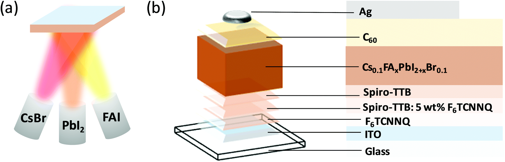 | ||
| Fig. 1 (a) Schematic diagram of the triple-source co-evaporation system used in this study. (b) Schematic diagram of the photovoltaic device structure. | ||
Experimental
Materials
Photovoltaic device fabrication and characterisation
![[thin space (1/6-em)]](https://www.rsc.org/images/entities/char_2009.gif) :1, while the rate of FAI was varied to achieve the ‘FAI-poor’ (1.50 Å s−1), ‘stoichiometric’ (1.55 Å s−1) and ‘FAI-rich’ (1.60 Å s−1) conditions. Finally, the samples were transferred into a third vacuum chamber (CreaPhys GmbH, Germany) for the deposition of a C60 (20 nm) electron extraction layer, followed by an 80 nm thick Ag cathode. The completed photovoltaic devices were encapsulated in a nitrogen-filled glovebox using a transparent encapsulation glass, secured by UV-hardened epoxy glue. For post-annealed devices, a 10 min 100 °C post-annealing procedure on encapsulated devices was followed.
:1, while the rate of FAI was varied to achieve the ‘FAI-poor’ (1.50 Å s−1), ‘stoichiometric’ (1.55 Å s−1) and ‘FAI-rich’ (1.60 Å s−1) conditions. Finally, the samples were transferred into a third vacuum chamber (CreaPhys GmbH, Germany) for the deposition of a C60 (20 nm) electron extraction layer, followed by an 80 nm thick Ag cathode. The completed photovoltaic devices were encapsulated in a nitrogen-filled glovebox using a transparent encapsulation glass, secured by UV-hardened epoxy glue. For post-annealed devices, a 10 min 100 °C post-annealing procedure on encapsulated devices was followed.
External quantum efficiency (EQE) spectra of the thermally evaporated devices were measured using a monochromator (Cornerstone 260), a chopped and collimated halogen lamp light source and a lock-in amplifier (Signal Recovery SR 7265). The setup was calibrated using a reference diode (Hamamatsu S1337). The current density–voltage (J–V) characteristics were recorded using a Keithley 2400 source measure unit using a solar simulator 16S-003-300 (Solarlight Company Inc.) that was tuned to a mismatch corrected light intensity, determined by an outdoor reference cell (Fraunhofer Institute for Solar Energy Systems, Freiburg, Germany). The active area of the solar cells was determined using optical microscopy to be approximately 6.44 mm2.
:FAI:PbI2:PbBr2 powder by molar ratio of 2:18:19:1 in DMSO:DMF (anhydrous, 99.8% and 99.9%, respectively) v/v 1:4 solvent mixture. The perovskite solution was spin-coated at 1000 rpm 10 s and 6000 rpm 30 s. During the second step, 130 μl anisole (anhydrous, 99.7%) were dispensed onto the film as anti-solvent 5 s prior to the end of the spin-coating step. The samples were annealed at 100 °C for 10 min. Next, the samples were transferred into a nitrogen-filled glovebox, where PC61BM (20 mg ml−1 dissolved in anhydrous chlorobenzene, 99.8%) was dynamically spin-coated at 2000 rpm for 30 s followed by a 10 min annealing at 100 °C. Finally, a bathocuproine (BCP) (0.5 mg ml−1 dissolved in anhydrous isopropanol, 99.5%) hole-blocking layer was spin-coated at 4000 rpm for 30 s, following by an 80 nm thermally evaporated Ag cathode (Mantis evaporator, base pressure of 10−7 mbar).
EQE spectra of the solution-processed devices were measured with the monochromatic light of a halogen lamp from 375 nm to 850 nm, which was calibrated using a NIST-traceable Si diode (Thorlabs). J–V characteristics were measured using a computer controlled Keithley 2450 Source Measure Unit under a simulated AM 1.5 sunlight with 100 mW cm−2 irradiation (Abet Sun 3000 Class AAA solar simulator). The light intensity was calibrated using a Si reference cell (NIST traceable, VLSI) and corrected by measuring the spectral mismatch between the solar spectrum, the spectral response of the perovskite solar cell, and the reference cell. The cells were scanned from forward bias (1.2 V) to short circuit and reverse at a rate of 0.25 V s−1 by employing a mask to eliminate the overestimation of the photocurrent. No preconditioning was applied prior to measurements. The active area of the devices was 4.5 mm2.
UV-vis absorption and photoluminescence (PL) measurements
A Shimadzu UV-3100 spectrometer was used in the ultraviolet-visible (UV-vis) absorption spectra. PL spectra were measured by exciting the 280 nm-thick samples with a 1.3 ns pulse laser (wavelength: 355 nm; intensity: 100 μJ cm−2; repetition rate: 10 kHz), and collecting photons at the opposite side from the excitation.Scanning electron microscopy (SEM)
A SEM (Gemini 500, ZEISS, Oberkochen, Germany) was used to acquire the surface morphology images at an acceleration voltage of 3 kV.X-ray diffraction (XRD)
XRD measurements were conducted in ambient using a Bruker D8 Discover diffractometer equipped with a 1.6 kW Cu-Anode (λ = 1.54060 Å) and a LYNXEYE_XE_T detector operated in 0D-Mode. The coupled θ/2θ scans (from 2θ = 5°–45°, step size 0.01°, 0.6 s per step) were measured in parallel beam geometry (goniometer radius 420 mm) with a 10 mm beam mask. The measured data was background corrected, the contribution of Kα2 was stripped using the Diffrac.Eva V4.3 software and the reflections were fitted using split-pseudo Voigt functions utilizing the Rigaku SmartLab Studio II software to extract peak position and FWHM.Results and discussion
Optical properties
To investigate the effect of FAI excess or deficiency on the optical properties of the perovskite films, their absorption and emission properties were characterised. Fig. 2a–c show the UV-vis absorption spectra of the FAI-poor, stoichiometric and FAI-rich perovskites as-deposited and after annealing. All samples show spectrally similar absorption features and a similar optical bandgap. The bandgap of the as deposited films is unaffected by the subtle changes in composition and is equal to 1.58 eV, in agreement with previous work on chemical vapour deposited Cs0.1FA0.9PbI2.9Br0.1.37 No change in bandgap is observed upon annealing, apart from the FAI-rich samples, in which it is slightly decreased. Interestingly, while stoichiometric samples show little variation in absorption upon annealing, FAI-poor and FAI-rich perovskites exhibit significant and opposite changes in their absorption. The absorption of the FAI-poor samples is increased, suggesting that annealing promotes crystallisation of the perovskite film. On the other hand, the annealing reduces the absorption of FAI-rich samples possibly due to degradation.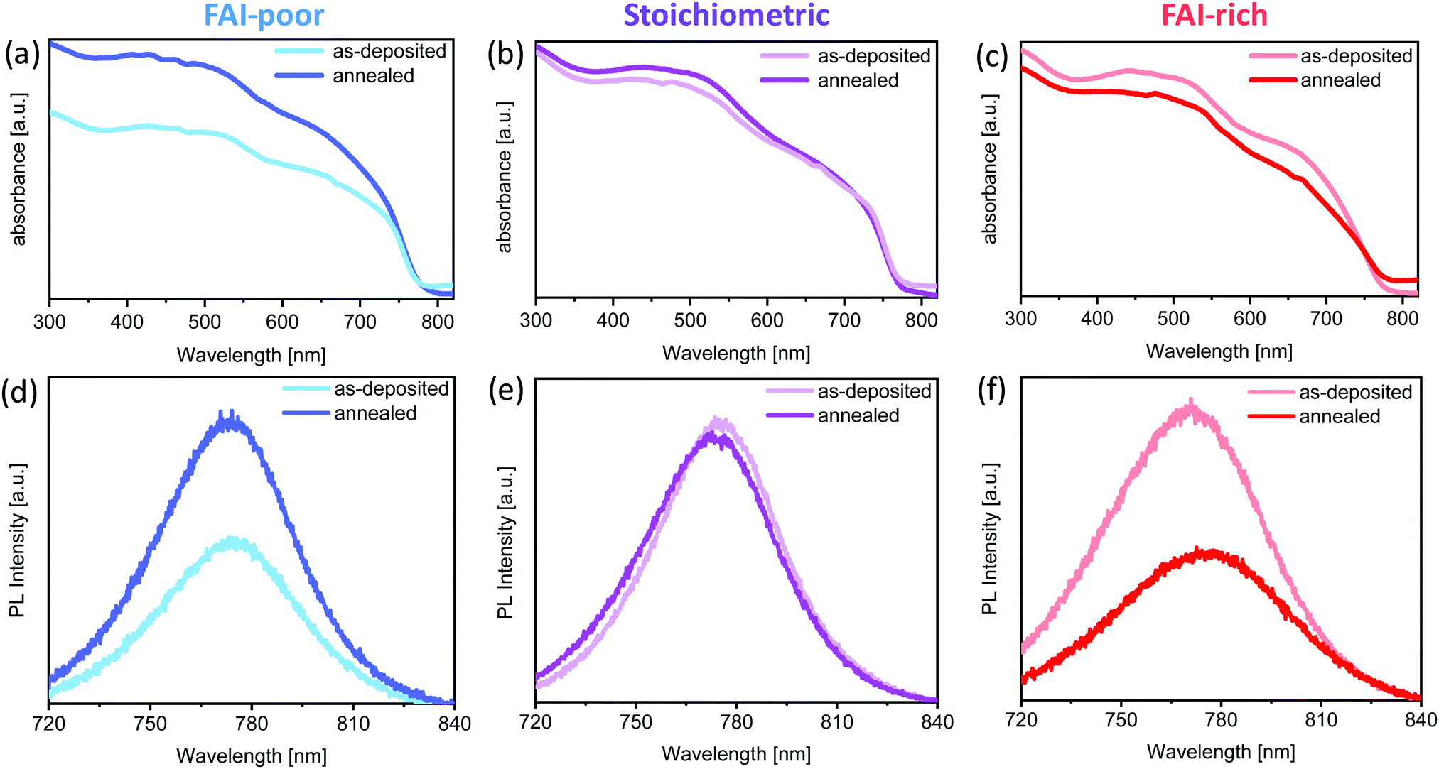 | ||
| Fig. 2 Absorption and photoluminescence emission spectra of (a)/(d) FAI-poor, (b)/(e) Stoichiometric and (c)/(f) FAI-rich perovskite samples prepared on glass substrates before and after annealing at 100 °C, respectively. | ||
PL measurements of the samples show a similar trend. Stoichiometric samples show nearly no change in emission peak position and intensity. On the other hand, the PL of the FAI-poor perovskite samples is enhanced upon annealing, nearly doubling in intensity. Similar to the loss of absorption, FAI-rich samples exhibit a substantial decrease in PL, which is slightly red-shifted in agreement with the small decrease in the optical bandgap.
Microstructure and crystallinity
SEM was used to image the microstructure of the perovskite films (Fig. 3a–f). While all evaporated layers appear smooth and homogeneous, the average grain size varies gradually between samples with different FAI content. Generally, FAI-poor perovskite films consist of small grains (below 100 nm in diameter), which are only slightly increased after annealing. Stoichiometric as-deposited samples show a similarly small grain structure, however, upon annealing the grains are doubled in size. The biggest change in grain size is observed in the FAI-rich samples, in which the initially already large grains (approximately 200 nm) are tripled in size upon annealing. The average grain sizes are summarised in Fig. 3g.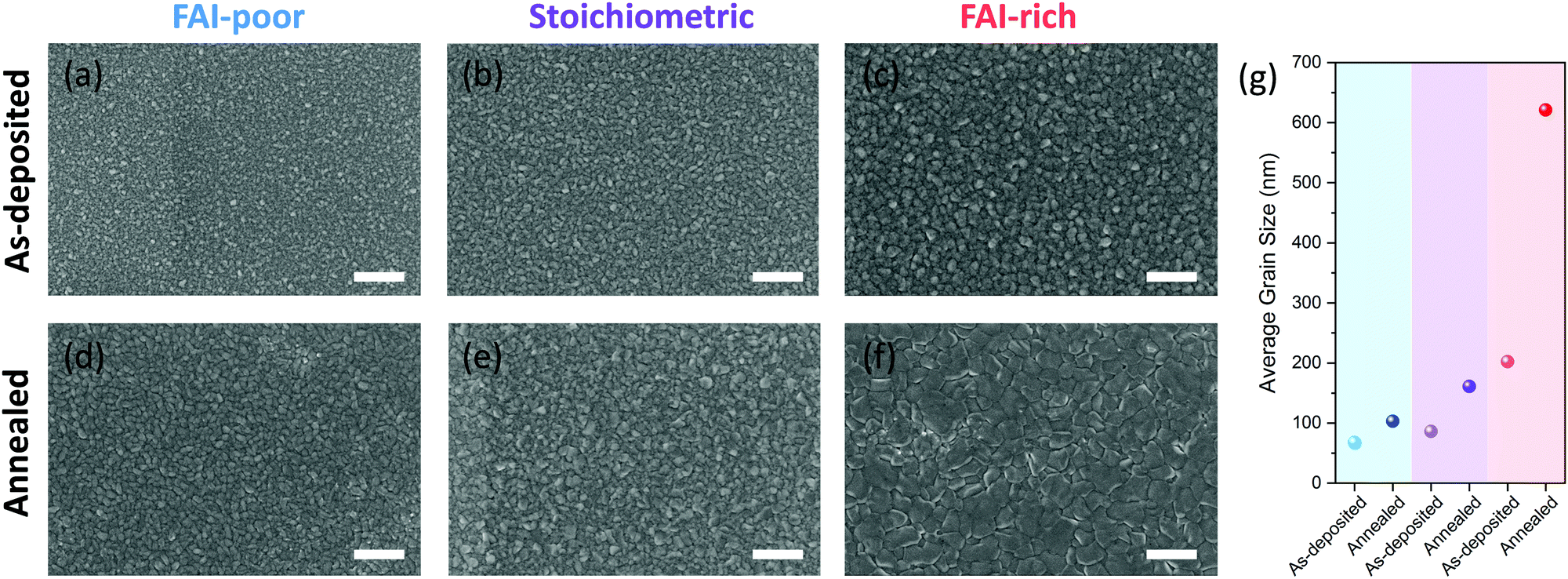 | ||
| Fig. 3 Scanning electron microscopy images of (a)/(d) FAI-poor, (b)/(e) Stoichiometric (c)/(f) FAI-rich perovskite samples prepared on glass substrates before and after annealing at 100 °C, respectively. Scale bar is 1 μm. (g) Summary of the average grain size. | ||
The evolution in microstructure is accompanied by structural changes of the perovskite films. XRD measurements showed that, as expected, the as-deposited FAI-poor perovskite films contain a small amount of residual PbI2 along with broad (100) and (200) reflections originating from the perovskite (Fig. 4a), in agreement with previous reports.38 Importantly, we only observe reflections in the diffraction pattern that correspond to the photovoltaically active black phase and no reflections that correspond to the inactive, yellow phase. Upon annealing, the intensity of these peaks is dramatically increased and the peaks are reduced in width, suggesting a higher long-range order. Additionally, the reflections shift to lower d-values, indicating a better and more compact crystal packing (Table 1). Stoichiometric samples show a similar trend, although the as-deposited samples do not show phase-separated PbI2, which appears only after the annealing step (Fig. 4b). Conversely, the FAI-rich samples show intense (100) and (200) reflections, which upon annealing are reduced in intensity, suggesting that the material decomposes upon annealing (Fig. 4c). Considering that no new reflections are observed, it is likely that the decomposition products are amorphous in nature. We observe that increasing the iodide content in the perovskite layers (by increasing the FAI evaporation rate), the diffraction pattern shifts to larger d values (smaller 2θ), which originates from the larger size of the iodide ions as compared to the smaller bromide ion. A similar trend has been shown by Kovalenko and co-workers for single crystals of variable composition CsxFA1−xPbI3−yBry, where an increase in the bromide content resulted in a decrease in the d spacing.38 Interestingly, the absence of reflections for other Bragg series suggests a high degree of preferred orientation in the evaporated perovskite films, similar to what has been observed by Herz and co-workers for solution-processed MA-free perovskites films with Cs0.1FA0.9 cation composition.39 We note that this is starkly different from the random orientation observed in thermally evaporated films reported by Gil-Escrig et al., in which the Cs0.5FA0.5 cation composition was employed.33
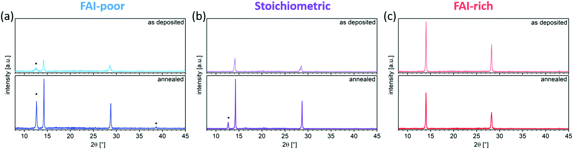 | ||
| Fig. 4 X-ray diffraction patterns of (a) FAI-poor, (b) stoichiometric, and (c) FAI-rich perovskite samples prepared on glass substrates before and after annealing at 100 °C. Reflections originating from PbI2 are marked with a *. | ||
| Stoichiometry | Annealing | Position [°] | d-value [Å] | FWHM [°] | Position [°] | d-value [Å] | FWHM [°] |
|---|---|---|---|---|---|---|---|
| (100) reflection | (200) reflection | ||||||
| FAI-poor | As-deposited | 14.21 | 6.229 | 0.228 | 28.57 | 3.121 | 0.403 |
| Annealed | 14.27 | 6.200 | 0.102 | 28.77 | 3.101 | 0.138 | |
| Stoichiometric | As-deposited | 14.14 | 6.258 | 0.219 | 28.21 | 3.161 | 0.212 |
| Annealed | 14.25 | 6.209 | 0.092 | 28.71 | 3.107 | 0.097 | |
| FAI-rich | As-deposited | 14.00 | 6.320 | 0.148 | 28.23 | 3.158 | 0.217 |
| Annealed | 14.03 | 6.306 | 0.132 | 28.27 | 3.155 | 0.184 | |
Taken together the optical and structural characterisation results reveal that the annealing step is only beneficial to the FAI-poor and, to a lesser degree, for the stoichiometric samples, while FAI-rich samples appear to be negatively impacted. It is particularly interesting that the appearance of large grains as observed by SEM for the annealed FAI-rich samples does not coincide with high crystallinity or absorbance. One possible explanation is the fact that SEM images only the surface grain structure, while it is possible that the bulk of the film consists of smaller domains with poor crystallinity. Moreover, recent studies revealed that grains as visualised by SEM may not represent the crystallographic grains as can be imaged for example by electron backscatter diffraction (EBSD).40 Consequently, in our case, it is possible that although the grains as shown by SEM appear to be large, they in fact consist of much smaller crystallites.
Photovoltaic performance
To investigate the photovoltaic performance of the perovskite layers, 280 nm thick layers were incorporated in solar cells with an inverted device architecture using thermally evaporated extraction layers (Fig. 1b). As-deposited FAI-poor devices show a relatively poor performance achieving in average only 8 mA cm−2 as short-circuit current (JSC) and ∼45% in fill factor (FF). The open-circuit voltage (VOC) is also relatively low at 0.93 V, resulting in power conversion efficiencies ranging from 3% to 4% (Fig. 5). Annealing results in a remarkable improvement in device performance with significant enhancements in all the photovoltaic parameters. Most pronounced are the change in JSC, which is more than doubled, reaching up to 19 mA cm−2, and the change in FF, which reaches over 70%. Together with a 150 mV increase in the VOC, the devices reach up to 14% in power conversion efficiency. | ||
| Fig. 5 Photovoltaic performance parameters (VOC, JSC, FF and PCE) of FAI-poor (blue), stoichiometric (purple) and FAI-rich (red) photovoltaic devices before and after annealing at 100 °C. | ||
As-deposited stoichiometric solar cells show a significantly higher photovoltaic performance as compared to the as-deposited FAI-poor devices, and a far smaller enhancement upon annealing. The VOC of the devices remains largely unchanged upon annealing at an average value of 1.07 V. Similarly, the fill factor is only slightly increased from an initial value of 70% to 75%. The average JSC is increased from 15 mA cm−2 to 17 mA cm−2, resulting in an overall enhancement in the average PCE of 11% to 13% and a maximum PCE of 15%.
Unlike the previous two cases, as-deposited FAI-rich solar cells show a moderate photovoltaic performance, which is significantly decreased upon annealing. In particular, a stark reduction in JSC and VOC leads to a decrease in the PCE from an initial average value of 9% to only 2% after annealing.
The changes in the photovoltaic performance are in agreement with the variations observed in the optical and structural properties of the perovskite layers upon annealing. The strong improvement in the case of the FAI-poor devices originates from the increase in perovskite layer crystallinity, absorption and emission efficiency. While the first two contribute to the increase in JSC, the latter represents a suppression in the rate of non-radiative recombination, which contributes to the increase in VOC.41 The enhancement in the JSC of the stoichiometric devices is related to the increase in absorption and crystallinity of the perovskite layers upon annealing. While the reduction in the absorption, emission and crystallinity of the FAI-rich films upon annealing is in agreement with the decline of their photovoltaic performance, the remarkable increase in the grain size as observed by SEM (Fig. 3f) seems unexpected in light of the deterioration of their other properties. Interestingly, it was recently reported that evaporated MAPbI3 films with large grain structure also result in low photovoltaic performance,42 suggesting further investigation is required to elucidate the relationship of grain size and photovoltaic performance in evaporated perovskite solar cells.
Active layer thickness optimization and comparison to solution processed devices
Thus far, we identified that stoichiometric devices lead to the highest photovoltaic performance. To further enhance the efficiency of the devices, we optimised their active layer thickness. Fig. 6 shows the evolution of the photovoltaic performance parameters of stoichiometric devices with 280 nm, 400 nm and 600 nm active layer thickness before and after annealing. 400 nm thick devices show an overall higher performance than that of 280 nm thick devices, due to an increase in the JSC, with minimal impact on VOC and FF. However, increasing the thickness further to 600 nm hampers the photovoltaic performance, with strong reductions in all the photovoltaic parameters. It is noteworthy that unlike the case with the thinner active layers, annealing of the thick devices reduces their photovoltaic performance further, especially in the device current.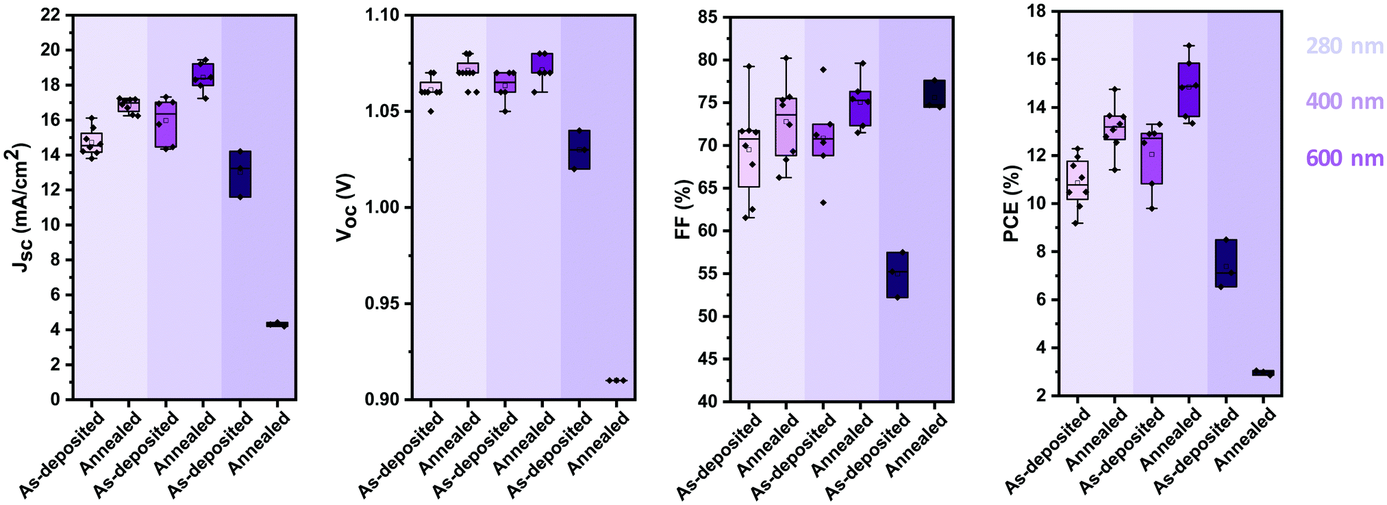 | ||
| Fig. 6 Photovoltaic performance parameters (VOC, JSC, FF and PCE) of stoichiometric photovoltaic devices with active layers of 280 nm, 400 nm and 600 nm before and after annealing at 100 °C. | ||
The best performing thermally evaporated solar cell was obtained for a 400 nm thick active layer upon annealing. The EQE, the J–V characteristics and the maximum power point (MPP) tracking are shown in Fig. 7a–c, respectively. The EQE spectrum shows photovoltaic response at or surpassing 80% between 400 nm and 730 nm, resulting in an integrated short-circuit current of 19.2 mA cm−2, in good agreement with the measured JSC (Fig. 7b). The J–V characteristics reveal the presence of hysteresis, with the forward scan resulting in higher performance than the backward scan, similar to previous reports on MA-free evaporated solar cells.31 While the VOC differs only slightly between the two scans, the FF is strongly influenced, reducing from nearly 80% to only 69% for the backward scan. The power conversion efficiency reaches 16.6% and 14.1% in the forward and backward scans, respectively, significantly surpassing the previously reported PCEs of 9.7% and 8.5% for MA-free evaporated solar cells.31 MPP tracking shows that an efficiency of 16.4% is stabilised after approximately 30 seconds.
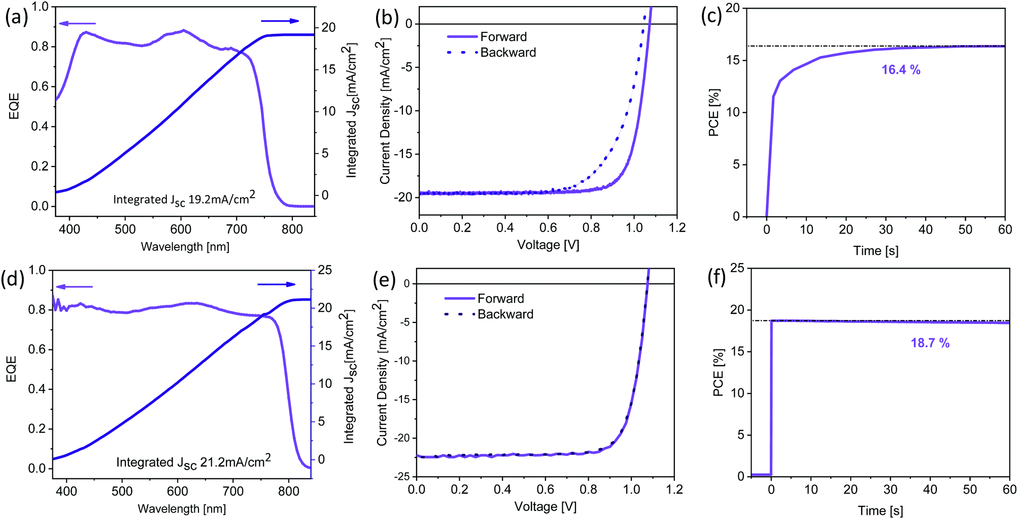 | ||
| Fig. 7 (a)/(d) External quantum efficiency and integrated current density, (b)/(e) J–V characteristics and (c)/(f) maximum power point tracking for champion thermally evaporated (top panels) and solution-processed (bottom panels) solar cells. The corresponding photovoltaic performance parameters are summarised in Table 2. | ||
To compare this performance with solution-processed Cs0.1FA0.9PbI2.9Br0.1 (XRD data is shown in Fig. S1, ESI†) solar cells, we fabricated devices in an inverted architecture with solution-processed hole extraction layer poly[bis(4-phenyl)(2,4,6-trimethylphenyl)amine] (PTAA) and electron extraction layer phenyl-C61-butyric acid methyl ester (PC61BM) capped by a hole-blocking layer bathocuproine (BCP) and a Ag cathode. While the EQE spectrum of the solution-processed device shows similar response of ≥80%, the spectrum extends to ∼825 nm (Fig. 7d), significantly further than the ∼775 nm previously observed for the thermally evaporated devices (Fig. 7a). This observation means that the optical properties of the solution-processed Cs0.1FA0.9PbI2.9Br0.1 films resemble those of single crystals of the same composition.38 As a consequence, the integrated JSC is enhanced and is predicted to be 21.2 mA cm−2. J–V characteristics show a similar VOC (1.07 V) despite the lower bandgap, suggesting significantly reduced non-radiative losses when compared to the thermally evaporated solar cells. While in both cases the FF is similar at ∼79%, solution-processed devices exhibit almost no hysteresis (Fig. 7e). The PCE of the solution-processed devices reaches 19.1% and 18.93% in the forward and reverse scans, respectively. MPP tracking (Fig. 7f) shows a stabilised efficiency of 18.7%, achieved nearly immediately after illumination. The photovoltaic performance parameters for the champion devices of both types are summarised in Table 2.
| Type | Scan direction | V OC [V] | J SC [mA cm−2] | FF [%] | PCE [%] |
|---|---|---|---|---|---|
| Thermally evaporated | Forward | 1.07 | 19.5 | 79.7 | 16.6 |
| Reverse | 1.05 | 19.5 | 68.8 | 14.1 | |
| Solution processed | Forward | 1.08 | 22.3 | 79.3 | 19.1 |
| Reverse | 1.08 | 22.3 | 78.6 | 18.9 |
There are many possible contributing factors to the differences in the photovoltaic performance of the solution-processed and thermally evaporated devices. For example, vacuum-processed perovskite films tend to be much smoother than those fabricated from solution. Hence, there can exist a benefit from light scattering in solution processed devices. However, the similarly high EQE of ∼80% that is achieved in both the solution- and the vacuum-processed devices suggests that the optical path lengths are sufficiently long in both types of devices and that the difference in the JSC originates from the wider absorption range of the solution-processed device. Another contributing factor can be the fact that both devices employ different charge extraction layers. The extraction layers in the thermally evaporated devices were selected following our previous work,24 in which we explored a broad range of hole extraction layers in perovskite solar cells and identified that Spiro-TTB lead to a high photovoltaic performance. In the case of the solution-processed devices, the chosen extraction layers are routinely used in high performance perovskite solar cells fabricated in an inverted architecture.43,44 Since neither the solution-processed nor the thermally evaporated extraction layers result in large energetic offsets to the perovskite active layer, the VOC in both types of devices are unlikely to be limited by the built-in potential of these solar cells.45 The presence of hysteresis solely in the J–V characteristics of the thermally evaporated devices, despite the use of a fullerene electron extraction layer, indicates that it is necessary to improve the perovskite quality and perovskite/extraction layer interface. To summarise, the higher efficiency achieved for the solution-processed devices demonstrates that further improvements in the deposition of thermally evaporated perovskites are required. In particular, the difference in the photovoltaic spectral response between the thermally evaporated and solution-processed devices highlights the need to optimise the composition of the former in order to improve the short-circuit current by extending their absorption towards the near infrared.
Conclusions
In conclusion, we fabricated and characterised thermally evaporated MA-free double cation double anion perovskite films and photovoltaic devices. By tuning the rate of FAI evaporation, we investigated the effect of deficiency or excess of FAI in these perovskites and studied the effect of annealing on the film properties and device performance. We find that the performance of FAI-poor and stoichiometric devices is improved upon annealing, while FAI-rich devices are negatively impacted. This is in agreement with the enhanced absorption, emission efficiency and crystallinity observed for the FAI-poor films, and the decrease in these properties for the FAI-rich layers. Overall, the highest efficiency is observed for annealed stoichiometric devices with a 400 nm thick active layer, reaching a maximum power conversion efficiency of 16.6%. While this value surpasses all previous reports on thermally evaporated MA-free perovskite solar cells, a comparison to solution-processed devices, which reach up to 19.1%, emphasises that further improvements both in perovskite layer composition and interfacial properties are required in order to enhance the efficiency of thermally evaporated perovskite solar cells.Conflicts of interest
There are no conflicts to declare.Acknowledgements
R. J. and Z. Z. are grateful for the financial support by the China Scholarship Council (Scholarship #201806070145 and #201806750012, respectively). C. C. is thankful for funding from Alexander von Humboldt foundation via Humboldt Research Fellowship for Postdoc Researchers. M. K. and F. N. are grateful for funding from the European Regional Development Fund (ERDF) and the Free State of Saxony in the framework of INeT project “Investigation of lead- and tin-free perovskite solar cells using vacuum techniques” (project number 100341673). K. L. and Y. V. thank the Deutsche Forschungsgemeinschaft (DFG) for funding in the framework of the special priority program SPP2196 (projects 〈PHIVE-X〉 #424090028 and 〈PERFECT PVs〉 #424216076, respectively). The authors are thankful to Prof. Jana Zaumseil (Heidelberg University) for access to software for XRD data analysis.References
- A. Kojima, K. Teshima, Y. Shirai and T. Miyasaka, J. Am. Chem. Soc., 2009, 131, 6050–6051 CrossRef CAS PubMed.
- M. Saliba, T. Matsui, J.-Y. Seo, K. Domanski, J.-P. Correa-Baena, M. K. Nazeeruddin, S. M. Zakeeruddin, W. Tress, A. Abate, A. Hagfeldt and M. Grätzel, Energy Environ. Sci., 2016, 9, 1989–1997 RSC.
- A. Dubey, N. Adhikari, S. Mabrouk, F. Wu, K. Chen, S. Yang and Q. Qiao, J. Mater. Chem. A, 2018, 6, 2406–2431 RSC.
- A.-N. Cho and N.-G. Park, ChemSusChem, 2017, 10, 3687–3704 CrossRef CAS PubMed.
- S. Shao and M. A. Loi, Adv. Mater. Interfaces, 2020, 7, 1901469 CrossRef CAS.
- https://www.nrel.gov/pv/cell-efficiency.html, accessed 22/03/2020.
- H. J. Snaith, A. Abate, J. M. Ball, G. E. Eperon, T. Leijtens, N. K. Noel, S. D. Stranks, J. T.-W. Wang, K. Wojciechowski and W. Zhang, J. Phys. Chem. Lett., 2014, 5, 1511–1515 CrossRef CAS PubMed.
- E. Erdenebileg, L. E. Scholz, A. Hofacker, C. Koerner and K. Leo, Energy Technol., 2017, 5(9), 1606–1611 CrossRef CAS.
- N. Tessler and Y. Vaynzof, ACS Appl. Energy Mater., 2018, 1, 676–683 CrossRef CAS.
- Q. Sun, P. Fassl, D. Becker-Koch, A. Bausch, B. Rivkin, S. Bai, P. E. P. E. Hopkinson, H. J. H. J. Snaith and Y. Vaynzof, Adv. Energy Mater., 2017, 7, 1700977 CrossRef.
- Q. Wang, B. Chen, Y. Liu, Y. Deng, Y. Bai, Q. Dong and J. Huang, Energy Environ. Sci., 2017, 10, 516–522 RSC.
- P. Fassl, V. Lami, A. Bausch, Z. Wang, M. T. Klug, H. J. Snaith and Y. Vaynzof, Energy Environ. Sci., 2018, 11, 3380–3391 RSC.
- M. Saliba, J.-P. Correa-Baena, C. M. Wolff, M. Solterfoht, N. Phung, S. Albrecht, D. Neher and A. Abate, Chem. Mater., 2018, 30(13), 4193–4201 CrossRef CAS.
- L. M. Falk, K. P. Goetz, V. Lami, Q. An, P. Fassl, J. Herkel, F. Thome, A. D. Taylor, F. Paulus and Y. Vaynzof, Energy Technol., 2020, 8, 1900737, DOI:10.1002/ente.201900737.
- I. A. Howard, T. Abzieher, I. M. Hossain, H. Eggers, F. Schackmar, S. Ternes, B. S. Richards, U. Lemmer and U. W. Paetzold, Adv. Mater., 2019, 31, 1806702 CrossRef PubMed.
- R. Swartwout, M. T. Hoerantner and V. Bulobic, Energy Environ. Mater., 2019, 2(2), 119–145 CrossRef CAS.
- N.-G. Park and K. Zhu, Nat. Rev. Mater., 2020, 33, DOI:10.1038/s41578-019-0176-2.
- H. Eggers, F. Schackmar, T. Abzieher, Q. Sun, U. Lemmer, Y. Vayznof, B. S. Richards, G. Hernandez-Sosa and U. W. Paetzold, Adv. Energy Mater., 2020, 10, 1903184 CrossRef CAS.
- G. Tong, H. Li, T. Zhang, C. Li, L. Yu, J. Xu, Y. Jiang, Y. Shi and K. Chen, Nano Energy, 2018, 48, 536–542 CrossRef CAS.
- C. Momblona, L. Gil-Escrig, E. Bandiello, E. M. Hutter, M. Sessolo, K. Lederer, J. Blochwitz-Nimoth and H. J. Bolink, Energy Environ. Sci., 2016, 9, 3456–3463 RSC.
- B. Qu and S. R. Forrest, Appl. Phys. Lett., 2018, 113, 053302 CrossRef.
- T. Moench, et al., in Molecular Devices for Solar Energy Conversion and Storage, Green Chemistry and Sustainable Technology, ed. H. Tian, et al., Springer Nature, Singapore, 2018 DOI:10.1007/978-981-10-5924-7_1.
- M. Liu, M. B. Johnston and H. J. Snaith, Nature, 2013, 501, 395–398 CrossRef CAS PubMed.
- L. E. Polander, P. Pahner, M. Schwarze, M. Saalfrank, C. Koerner and K. Leo, APL Mater., 2014, 2, 1–6 Search PubMed.
- G. Liang, H. Lan, P. Fan, C. Lan, Z. Zheng, H. Peng and J. Luo, Coatings, 2018, 8(8), 256 CrossRef.
- D. Perez-del-Rey, P. P. Boix, M. Sessolo, A. Hadipour and H. J. Bolink, J. Phys. Chem. Lett., 2018, 9, 1041–1046 CrossRef CAS PubMed.
- D. Perez-del-Rey, L. Gil-Escrig, K. P. S. Zanoni, C. Dreesen, M. Sessolo, P. B. Boix and H. J. Bolink, Chem. Mater., 2019, 31(17), 6945–6949 CrossRef CAS.
- A. Babaei, C. Dreessen, M. Sessolo and H. J. Bolink, RSC Adv., 2020, 10, 6640–6646 RSC.
- F. Palazon, D. Perez-del-Rey, B. Danekamp, C. Dreessen, M. Sessolo, P. P. Boix and H. J. Bolink, Adv. Mater., 2019, 31(39), 1902692 CrossRef PubMed.
- S.-Y. Hsiao, H.-L. Lin, W.-H. Lee, W.-L. Tsai, K.-M. Chiang, W.-Y. Liao, C.-Z. Ren-Wu, C.-Y. Chen and H.-W. Lin, Adv. Mater., 2016, 28(32), 7013–7019 CrossRef CAS PubMed.
- J. Borchert, R. L. Milot, J. B. Patel, C. L. Davies, A. D. Wright, L. M. Maestro, H. J. Snaith, L. M. Herz and M. B. Johnston, ACS Energy Lett., 2017, 2(12), 2799–2804 CrossRef CAS.
- C. Yi, J. Luo, S. Meloni, A. Boziki, N. Ashari-Astani, C. Graetzel, S. M. Zakeeruddin, U. Rothlisberger and M. Graetzel, Energy Environ. Sci., 2016, 9, 656–662 RSC.
- L. Gil-Escrig, C. Momblona, M.-G. La-Placa, P. P. Boix, M. Sessolo and H. J. Bolink, Adv. Energy Mater., 2018, 8(14), 1703506 CrossRef.
- J. M. Ball, L. Buizza, H. C. Sansom, M. D. Farrar, M. T. Klug, J. Borchert, J. Patel, L. M. Herz, M. B. Johnston and H. J. Snaith, ACS Energy Lett., 2019, 4(11), 2748–2756 CrossRef CAS.
- T. J. Jacobsson, J.-P. Correa-Baena, E. H. Anaraki, B. Philippe, S. D. Stranks, M. E. F. Bouduban, W. Tress, K. Schenk, J. Teuscher, J.-E. Moser, H. Rensmo and A. Hagfeldt, J. Am. Chem. Soc., 2016, 138(32), 10331–10343 CrossRef CAS PubMed.
- C. Bi, Y. Shao, Y. Yuan, Z. Xiao, C. Wang, Y. Gao and J. Huang, J. Mater. Chem. A, 2014, 2, 18508 RSC.
- L. Qiu, S. He, Y. Jiang, D.-Y. Son, L. K. Ono, Z. Liu, T. Kim, T. Bouloumis, S. Kayaoui and Y. Qi, J. Mater. Chem. A, 2019, 7, 6920–6929 RSC.
- O. Nazarenko, S. Yakunin, V. Morad, I. Cherniukh, M. Kovalenko and N. P. G. Asia, Materials, 2017, 9, e373 CAS.
- R. Rehman, D. P. McMeekin, J. B. Patel, R. L. Milot, M. B. Johnston, H. J. Snaith and L. M. Herz, Energy Environ. Sci., 2017, 10, 361–369 RSC.
- S. Jariwala, H. Sun, G. W. P. Adhyaksa, A. Lof, L. A. Muscarella, B. Ehrler, E. C. Garnett and D. S. Ginger, Joule, 2019, 3, 3048 CrossRef CAS.
- K. P. Goetz, A. D. Taylor, F. Paulus and Y. Vaynzof, Adv. Funct. Mater., 2020, 1910004, DOI:10.1002/adfm.201910004.
- K. B. Lohmann, J. B. Patel, M. U. Rothmann, C. Q. Xia, R. D. J. Oliver, L. M. Herz, H. J. Snaith and M. B. Johnston, ACS Energy Lett., 2020, 5, 710–717 CrossRef CAS PubMed.
- C. Xu, Z. Liu and E.-C. Lee, J. Mater. Chem. C, 2018, 6, 6975–6981 RSC.
- Q. An, Q. Sun, A. Weu, D. Becker-Koch, F. Paulus, S. Arndt, F. Stuck, A. S. K. Hashmi, N. Tessler and Y. Vaynzof, Adv. Energy Mater., 2019, 9(33), 1901257 CrossRef.
- N. Tessler and Y. Vaynzof, ACS Energy Lett., 2020, 5(4), 1260–1270 CrossRef CAS.
Footnote |
| † Electronic supplementary information (ESI) available. See DOI: 10.1039/d0tc01550d |
| This journal is © The Royal Society of Chemistry 2020 |