
 Open Access Article
 This Open Access Article is licensed under a Creative Commons Attribution-Non Commercial 3.0 Unported Licence
Evaluating the role of phenethylamine iodide as a novel anti-solvent for enhancing performance of inverted planar perovskite solar cells†
Christos
Zervos
*,
Marinos
Tountas
,
Konstantinos
Chatzimanolis
,
Christos
Polyzoidis
and
Emmanuel
Kymakis
 *
*
Department of Electrical & Computer Engineering, Hellenic Mediterranean University, Estavromenos, 71410 Heraklion, Greece. E-mail: czervos@hmu.gr; kymakis@hmu.gr
First published on 22nd April 2020
Abstract
Inverted perovskite solar cells (PSCs) have attracted much interest due to their improved operational stability in the past few years. However, despite the recent advances of their performance, they still suffer from low power conversion efficiencies with a reduced open-circuit voltage (Voc), as compared to PSCs with a regular structure, due to the presence of defect states. In this work, a promising and more effective strategy than the typical post-treatment passivation method is demonstrated for the decrease of nonradiative recombination in quadruple-cation RbCsMAFA inverted PSCs, through the employment of phenethylammonium iodide in the anti-solvent deposition step during the perovskite formation. As a result, a Voc value as high as 1.17 V is achieved, while control devices (where the typical chlorobenzene anti-solvent was used) exhibited a significantly lower Voc of 1.09 V. Additionally, the devices exhibited high moisture stability by maintaining nearly 80% of their initial efficiency for over 500 h exposure in ambient conditions.
1. Introduction
Inverted (p–i–n) perovskite solar cells (PSCs) have drawn a great interest in the last few years because they offer many advantages compared to the most commonly employed regular (n–i–p) architecture. Easy fabrication, low-temperature and low-cost solution process, negligible hysteresis characteristics, compatibility with flexible substrates and large-scale printing fabrication are amongst the merits of the inverted configuration.1–3 Moreover, the inverted structure has been employed in monolithic perovskite/silicon heterojunction tandem solar cells for raising efficiencies beyond the crystalline Si single-junction limit.4,5However, only very recently have a few research studies proved the potential of inverted devices for efficiency competition with the regular structure, exhibiting power conversion efficiencies (PCEs) exceeding 20%.6–8 The relatively low open circuit voltage (Voc) is the main limiting factor which impedes further improvement of the devices performance and is mainly attributed to the presence of defect states or recombination centers, both inside the perovskite bulk material and at the surrounded interfaces.1
Most of the reported strategies to decrease trap densities are based on either the introduction of dopants in the charge transport layers9–13 and in the perovskite film14,15 or the introduction of a passivation layer between the perovskite film and the electron or hole transport layers.8,16,17
In this context, Hanmandlu et al.6 recently reported the enhancement of efficiency and stability of methylammonium lead iodide (MAPbI3) PSCs by using CdSe/ZnS and CdS/ZnS quantum dots as passivation layers on the perovskite surface with the best obtained Voc value of 1.06 V. Zhang et al.7 showed that the passivation of the MAPbI3 perovskite surface by Lewis-acid-featured fullerene skeleton after iodide ionization (PCBB-3N-3I) can reduce trap-assisted recombination and improve Voc from 1.059 to 1.105 V, leading to superior device performance of inverted PSCs.7 In another approach, a 2D PEA2PbI4 capping layer was introduced on top of a Cs/FA/MA triple-cation perovskite film resulted in an increased Voc from 1.05 to 1.11 V.8
Thus, despite the recent advances of inverted PSCs there is still much room to ameliorate and maximize their performance reaching the same levels as their counterparts structured in the regular architecture. Here, we report the use of phenethylammonium iodide (PEAI) in the anti-solvent process as a route to increase the Voc and therefore the PCE of the device. We demonstrate that this method is superior to the typical passivation method applied on ready-formed perovskite films, leading to the decrease of trap densities and the increase of charge carrier lifetimes. As a result, the PSCs exhibited a high Voc increase from 1.09 V to 1.17 V and an enhanced PCE with a maximum value of 18.75%, and showed high moisture stability, demonstrating the effectiveness of the proposed strategy to achieve efficient and stable PSCs.
2. Results and discussion
Fig. 1a shows the planar inverted configuration structured as indium tin oxide (ITO) glass substrate/poly(trimethyl amine) (PTAA)/RbCsFAMA/PC70BM/bathocuproine (BCP)/Ag. The quadruple cation perovskite composition studied here was Rb0.04Cs0.05[(FA0.85MA0.15)]0.9Pb(I0.85Br0.15)3, referred as RbCsFAMA (FA: formamidinium; MA: methylammonium). The embedding of Rb+ and Cs+ into the mixed halide perovskite solar cells was employed to improve the performance and stability of devices.18 The experimental details can be found in the ESI† section. We investigated PSCs using PEAI in butanol treatment (1 mg ml−1) in the anti-solvent step during the perovskite formation and results compared with control devices where the typical chlorobenzene (CB) anti-solvent was employed, as detailed in the Experimental section. Additionally, the conventional passivation method applied in control devices was also studied where a PEAI layer was post-deposited by spin-coating on top of the RbCsFAMA surface (after perovskite film formation), without any further processing.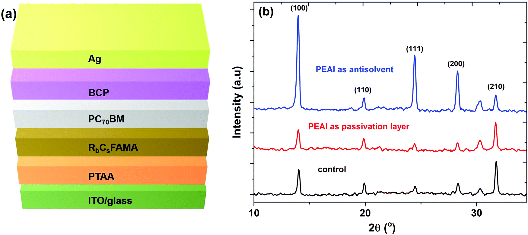 | ||
| Fig. 1 (a) The device structure studied in this work. (b) Conventional XRD patterns for the control, the film with post-deposited PEAI layer and the film with PEAI anti-solvent. | ||
We carried out X-ray Diffraction (XRD) measurements to examine the effect of PEAI on the crystal structure of the perovskite layer. The results are shown in Fig. 1b. We observe that both the PEAI-treated films, in the diffraction measurement range, have the same diffraction peaks as the control layer and no detectable signals that could be attributed to a 2D component formation appeared on the patterns, which is in agreement with similar previous reports.19,20 The possibility of 2D or quasi-2D peaks existence cannot be excluded for very low 2θ angles (<5°), however, such material information cannot be obtained due to the limited detection range of our diffractometer. Interestingly, we find that the intensities of (100) and (111) crystal plane's peaks for the film with PEAI anti-solvent are significantly increased compared to the other two layers, indicating the promotion of this specific crystal orientation of the film. In addition, the atomic force microscope image of the film with PEAI anti-solvent (Fig. S1, ESI†) revealed a smoother surface morphology with a root-mean-square (RMS) roughness of 13.7 nm, which is lower than that of the other films (RMS = 20.83 nm for the film with the post-deposited PEAI and 18.7 nm for the control). The high RMS of the post-deposited PEAI perovskite film is expected, since it is spin-coated on a rough perovskite surface (18.7 nm).19
The surface hydrophobicity was also tested by performing water contact angle (CA) measurements (Fig. S2, ESI†). CA for the control film is 79.4° and increased to 87.6° and 94.2° for the perovskite layers with PEAI anti-solvent and PEAI layer, respectively. This indicates that PEA+ ions assembled on the perovskite surface and grains boundaries and impeded the infiltration of water molecules to the inner layers, thus enhancing the hydrophobicity of the films. Finally, in order to gain more insight into the surface quality we conducted steady-state photoluminescence (PL) measurements (Fig. 2). Compared to the control film, PL exhibited a high increase in the intensity for both the PEAI treated films which implies a decreased number of nonradiative trap centres in the perovskite layers.19,21
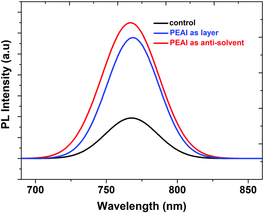 | ||
| Fig. 2 Emission peaks from steady-state photoluminescence spectra of the films excited under a 532 nm laser source. | ||
We fabricated PSCs to examine whether this modification in the basic structural and optical properties of the PEAI treated films may affect the performance of devices. Fig. 3a exhibits the typical current density–voltage (J–V) characteristics of the champion devices under AM 1.5 G illumination at a scan rate of 0.02 V s−1. It can be observed that the Voc of the device fabricated using PEAI as anti-solvent (1.17 V) was markedly higher than the Voc of the control device (1.09 V) and the PEAI post-treated device (1.11 V), while the short-circuit current (Jsc) is not substantially changing. No significant hysteresis was found in all the PSCs. Particularly, the control device exhibited a typical PCE of 17.47%, which is in close agreement with the latest reported values in planar inverted devices,7,20,22,23 a Jsc of 20.55 mA cm−2 and a fill factor (FF) of 77.99%. The efficiency of the device with the PEAI layer improved to 18.19% with a FF of 81.36% and a Jsc of 20.19 mA cm−2. However, the best performance PSC was obtained using the PEAI as anti-solvent exhibiting an increased PCE of 18.75% which mainly results from the significant Voc enhancement (Jsc and FF are 20.29 mA cm−2 and 79.89%, respectively). The optimal device processing conditions and materials needs to be developed in our future work in order to take advantage of the beneficial effect of PEAI anti-solvent and reach higher PCE values. Moreover, the integrated Jsc values from the external quantum efficiency are almost consistent with the value obtained from the solar simulator, as shown in Table 1. The statistical data from 20 devices of each structure, presented in Fig. 3b and c, verify the reproducibility of the PCE and Voc enhancement associated with the PEAI treatment. The figures of merit of the devices are depicted in Table 1.
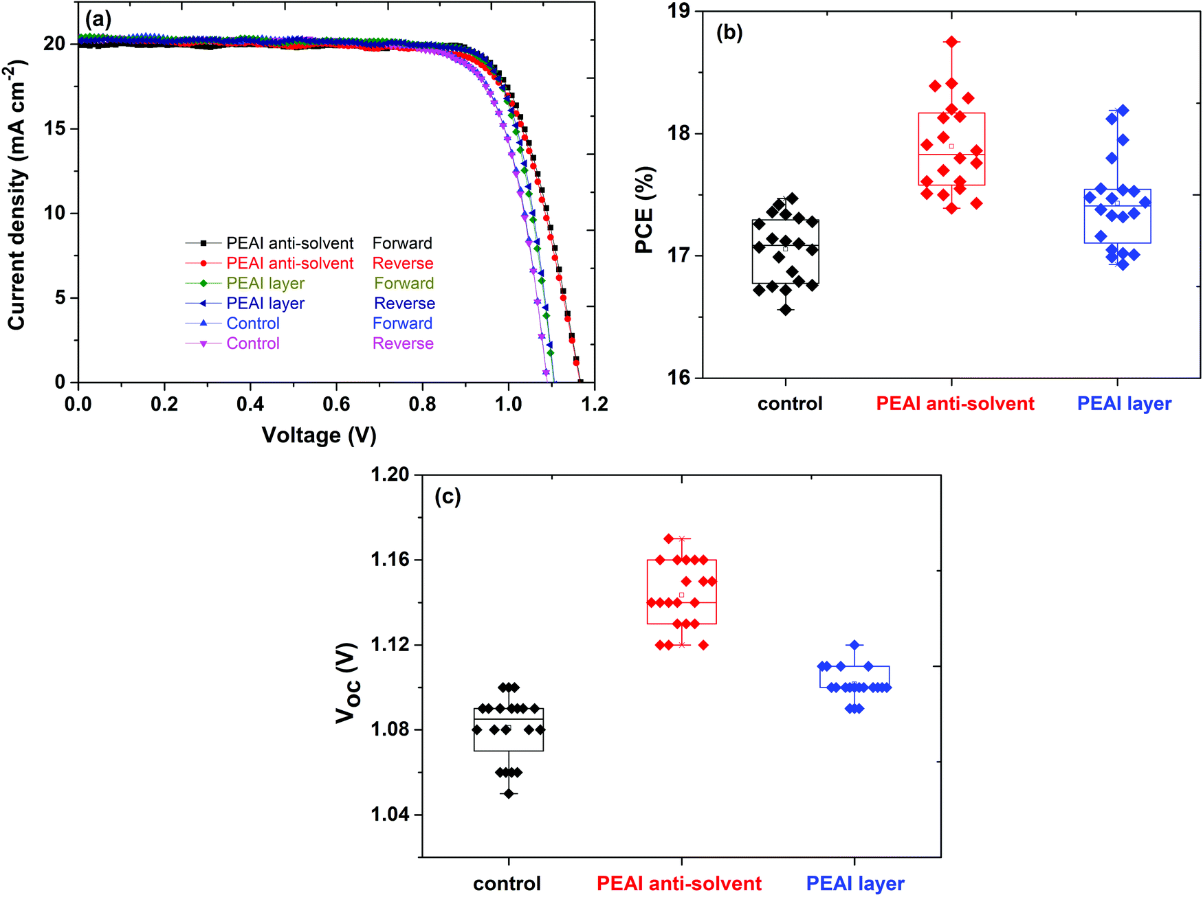 | ||
| Fig. 3 (a) J–V curves of the champion devices measured in both reverse and forward directions, with a scan rate of 0.02 V s−1, at 100 mW cm−2 simulated illumination (AM 1.5 G). (b) PCE and (c) Voc box charts for control and PEAI treated devices. | ||
| Device | V oc (V) | J sc (mA cm−2) | FF (%) | PCE (%) | J sc from EQE (mA cm−2) |
|---|---|---|---|---|---|
| Control | 1.08 (0.01) | 20.45 (0.44) | 77.22 (2.10) | 17.05 (0.27) | 20.09 |
| PEAI anti-solvent | 1.14 (0.01) | 19.94 (0.65) | 78.28 (1.43) | 17.85 (0.40) | 19.86 |
| PEAI layer | 1.10 (0.01) | 19.68 (0.44) | 80.41 (1.52) | 17.38 (0.44) | 19.81 |
To gain a deeper comprehension of the passivated effect of PEAI, we assessed trap-assisted recombination by testing the response of devices under different illumination intensities. The linear Jsc dependence with light intensity (Fig. S4, ESI†) shows that Jsc is proportional to the absorbed photons and is an evidence of smooth transport pathways of charge carriers in the devices. Fig. 4a exhibits that Voc can be also correlated linearly with slopes of 1.92 kT/q for the control device, 1.64 kT/q for the device with PEAI layer and 1.57 kT/q for the device treated with PEAI anti-solvent. It is widely accepted that when the ideality factor n is ranged between 1 and 2 this can be interpreted as a competition between free carrier radiative recombination and nonradiative trap-assisted carrier recombination.19,21,24 Consequently, the device with PEAI anti-solvent which exhibited the smallest deviation between Voc slope and the ideal value of kT/q (n = 1) has the lowest trap-assisted recombination rate compared to other devices. Furthermore, we extracted the charge recombination constants (τr) from the transient photovoltage decays measured at open circuit29 (Fig. 4b). It is well known that passivation effects result in increased recombination lifetimes in perovskite structures.30 The device with PEAI anti-solvent presents the slowest photovoltage decay time, in comparison with the device with PEAI layer and the control, confirming that this treatment results in the smallest charge recombination rate and the longest carrier lifetime, in accordance with the highest Voc obtained from J–V measurements. The calculated τr was 2.5 μs for the control and increased to the values of 6.8 and 8.2 μs for the PSCs with PEAI layer and PEAI anti-solvent, respectively.
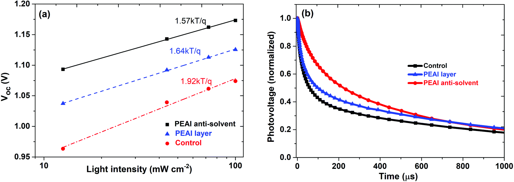 | ||
| Fig. 4 (a) Voc as a function of light intensity. (b) Normalized transient photovoltage decay measurements for the RbCsFAMA devices with and without PEAI treatment. | ||
Finally, the moisture stability of devices was tested for more than 500 h. The unencapsulated PSCs were stored at room temperature with 60 ± 10% relative humidity (RH) in dark conditions. As shown in Fig. 5, control devices degraded rapidly and lost almost half of their initial PCE at the end of 500 h. On the other hand, the PEAI-treated devices possess high moisture resistance retaining ∼80% of the initial PCE. Particularly, the PCE of the device with PEAI as anti-solvent exhibited the best behaviour showing a decreased trend in the first 72 h and then the performance was almost stabilized for over 500 h. These results agree with our previous contact angle measurements confirming the hydrophobic characteristic of PEA, which act as an impediment against moisture penetration into the inner perovskite layer hampering the degradation process.
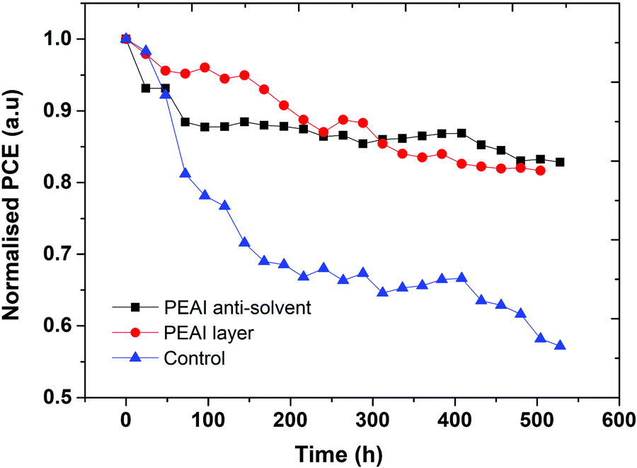 | ||
| Fig. 5 Moisture stability testing of devices up to 500 hours’ storage time. | ||
Our observations clearly show that the utilization of PEAI in the anti-solvent step can be much more beneficial, in terms of device performance, than the typical passivation applied on ready-formed perovskite layers. This result can be explained by taking into account not only the passivation effect but also the preferred crystal growth orientation. The PEA+ ions when introduced in the perovskite during the anti-solvent process, resulted in a ∼5 times higher XRD intensity of the (100) plane and also a rise of the (111) surface, compared to other films (Fig. 1b). Previous works have demonstrated that the PCE of PSCs can be influenced by controlling the crystal growth direction and the orientation of the facets.21,25 Zheng et al.21 recently reported that alkylamine ligands, when directly introduced into the perovskite precursor, can promote a (100)-favourable grain orientation film that is of lower defect density than a randomly oriented layer, resulting in an enhance performance compared to the conventional passivation technique. In our work, the full width at half maximum values of the (100) XRD peaks for all the films are almost the same (∼0.25°). Thus, we can exclude the effect of grain size as a main contributor of the best performance devices with PEAI as anti-solvent.
We believe that, similar to other researchers,21,25–28 the enhanced PCE is also facet-dependent, since different crystallographic facets may have different tendencies towards defect formation.21,25 More sensitive characterization methods could verify this conclusion and further investigations are ongoing.
3. Conclusions
In summary, we find that PEAI when used as an anti-solvent can play a more essential role to ameliorate the structural and optoelectronic properties of RbCsFAMA perovskite films, leading to a significant increase of the Voc of the devices, compared to post-treatment passivation. We attribute our findings partially to the microscopic structure and the orientation of grains in the perovskite films, which may impinge on the macroscopic PCE of the devices, combined with the passivation effect of trap states. Finally, the encapsulation-free PEAI treated PSCs exhibited enhanced moisture resistance retaining ∼80% of their initial PCE after 500 h of storage in dark conditions and a 60 ± 10% RH, compared to the 45% rapid loss of control devices. The optimization of device fabrication and the processing of the high crystalline perovskite absorber plays a very important role towards reliable devices performance31 and will be considered in our future work. Moreover, a better understanding of the dependence of performance and defect states on the control of crystal growth direction will be essential for boosting the PCE of inverted PSCs.Conflicts of interest
There are no conflicts to declare.Acknowledgements
This research has been co-financed by the European Union and Greek national funds through the Operational Program Competitiveness, Entrepreneurship and Innovation, under the call RESEARCH – CREATE – INNOVATE (project code: T1EDK-01082).References
- D. Luo, W. Yang, Z. Wang, A. Sadhanala, Q. Hu, R. Su, R. Shivanna, G. F. Trindade, J. F. Watts, Z. Xu, T. Liu, K. Chen, F. Ye, P. Wu, L. Zhao, J. Wu, Y. Tu, Y. Zhang, X. Yang, W. Zhang, R. H. Friend, Q. Gong, H. J. Snaith and R. Zhu, Science, 2018, 360, 1442 CrossRef CAS PubMed.
- W. Hu, C. Y. Xu, L. B. Niu, A. M. Elseman, G. Wang, D. B. Liu, Y. Q. Yao, L. P. Liao, G. D. Zhou and Q. L. Song, ACS Appl. Mater. Interfaces, 2019, 11, 22021 CrossRef CAS PubMed.
- H. Wu, C. J. Zhang, K. X. Ding, L. J. Wang, Y. L. Gao and J. L. Yang, Org. Electron., 2017, 45, 302 CrossRef CAS.
- L. Mazzarella, Y.-H. Lin, S. Kirner, A. B. Morales-Vilches, L. Korte, S. Albrecht, E. Crossland, B. Stannowski, C. Case, H. J. Snaith and R. Schlatmann, Adv. Energy Mater., 2019, 9, 1803241 CrossRef.
- M. Jošt, E. Köhnen, A. B. Morales-Vilches, B. Lipovšek, K. Jäger, B. Macco, A. AlAshouri, J. Krč, L. Korte, B. Rech, R. Schlatmann, M. Topič, B. Stannowski and S. Albrecht, Energy Environ. Sci., 2018, 11, 3511 RSC.
- C. Hanmandlu, S. Swamy, A. Singh, H.-A. Chen, A. Mohapatra, C.-C. Liu, C.-S. Lai, C.-W. Pao, P. Chen and C. W. Chu, J. Mater. Chem. A, 2020, 8, 5263 RSC.
- M. Zhang, Q. Chen, R. Xue, Y. Zhan, C. Wang, J. Lai, J. Yang, H. Lin, J. Yao, Y. Li, L. Chen and Y. Li, Nat. Commun., 2019, 10, 4593 CrossRef PubMed.
- P. Chen, Y. Bai, S. Wang, M. Lyu, J.-H. Yun and L. Wang, Adv. Funct. Mater., 2018, 28, 1706923 CrossRef.
- M. M. Tavakoli, P. Yadav, R. Tavakoli and J. Kong, Adv. Energy Mater., 2018, 8, 1800794 CrossRef.
- D. Yang, X. Zhou, R. Yang, Z. Yang, W. Yu, X. Wang, C. Li, S. Liu and R. P. H. Chang, Energy Environ. Sci., 2016, 9, 3071 RSC.
- F. Giordano, A. Abate, J. P. Correa Baena, M. Saliba, T. Matsui, S. H. Im, S. M. Zakeeruddin, M. K. Nazeeruddin, A. Hagfeldt and M. Graetzel, Nat. Commun., 2016, 7, 10379 CrossRef CAS PubMed.
- G. Kakavelakis, T. Maksudov, D. Konios, I. Paradisanos, G. Kioseoglou, E. Stratakis and E. Kymakis, Adv. Energy Mater., 2017, 7, 1602120 CrossRef.
- A. Agresti, S. Pescetelli, L. Cinà, D. Konios, G. Kakavelakis, E. Kymakis and A. D. Carlo, Adv. Funct. Mater., 2016, 26, 2686 CrossRef CAS.
- X. Li, W. Zhang, Y.-C. Wang, W. Zhang, H.-Q. Wang and J. Fang, Nat. Commun., 2018, 9, 3806 CrossRef PubMed.
- M. Abdi-Jalebi, Z. Andaji-Garmaroudi, S. Cacovich, C. Stavrakas, B. Philippe, J. M. Richter, M. Alsari, E. P. Booker, E. M. Hutter, A. J. Pearson, S. Lilliu, T. J. Savenije, H. Rensmo, G. Divitini, C. Ducati, R. H. Friend and S. D. Stranks, Nature, 2018, 555, 497 CrossRef CAS PubMed.
- X. Zheng, B. Chen, J. Dai, Y. Fang, Y. Bai, Y. Lin, H. Wei, X. C. Zeng and J. Huang, Nat. Energy, 2017, 2, 17102 CrossRef CAS.
- Y. H. Lee, J. Luo, M.-K. Son, P. Gao, K. T. Cho, J. Seo, S. M. Zakeeruddin, M. Grätzel and M. K. Nazeeruddin, Adv. Mater., 2016, 28, 3966 CrossRef CAS PubMed.
- M. Saliba, T. Matsui, K. Domanski, J.-Y. Seo, A. Ummadisingu, S. M. Zakeeruddin, J.-P. Correa-Baena, W. R. Tress, A. Abate, A. Hagfeldt and M. Grätzel, Science, 2016, 354, 206 CrossRef CAS PubMed.
- Q. Jiang, Y. Zhao, X. Zhang, X. Yang, Y. Chen, Z. Chu, Q. Ye, X. Li, Z. Yin and J. You, Nat. Photonics, 2019, 13, 460 CrossRef CAS.
- N. Li, Z. Zhu, Q. Dong, J. Li, Z. Yang, C.-C. Chueh, A. K.-Y. Jen and L. Wang, Adv. Mater. Interfaces, 2017, 4, 1700598 CrossRef.
- X. Zheng, Y. Hou, C. Bao, J. Yin, F. Yuan, Z. Huang, K. Song, J. Liu, J. Troughton, N. Gasparini, C. Zhou, Y. Lin, D.-J. Xue, B. Chen, A. K. Johnston, N. Wei, M. N. Hedhili, M. Wei, A. Y. Alsalloum, P. Maity, B. Turedi, C. Yang, D. Baran, T. D. Anthopoulos, Y. Han, Z.-H. Lu, O. F. Mohammed, F. Gao, E. H. Sargent and O. M. Bakr, Nat. Energy, 2020, 1–10, DOI:10.1038/s41560019-0538-4.
- D. Yang, X. Zhang, K. Wang, C. Wu, R. Yang, Y. Hou, Y. Jiang, S. Liu and S. Priya, Nano Lett., 2019, 19, 3313 CrossRef CAS PubMed.
- X. Zheng, B. Chen, J. Dai, Y. Fang, Y. Bai, Y. Lin, H. Wei, X. C. Zeng and J. Huang, Nat. Energy, 2017, 2, 17102 CrossRef CAS.
- D. Yang, R. Yang, K. Wang, C. Wu, X. Zhu, J. Feng, X. Ren, G. Fang, S. Priya and S. (Frank) Liu, Nat. Commun., 2018, 9, 3239 CrossRef PubMed.
- S. Y. Leblebici, L. Leppert, Y. Li, S. E. R-Lillo, S. Wickenburg, E. Wong, J. Lee, M. Melli, D. Ziegler, D. K. Angell, D. F. Ogletree, P. D. Ashby, F. M. Toma, J. B. Neaton, I. D. Sharp and A. Weber-Bargioni, Nat. Energy, 2016, 1, 16093 CrossRef CAS.
- S. Jariwala, H. Sun, G. W. P. Adhyaksa, A. Lof, L. A. Muscarella, B. Ehrler, E. C. Garnett and D. S. Ginger, Joule, 2019, 3, 3048 CrossRef CAS.
- L. Zhang, Y. Liu, X. Ye, Q. Han, C. Ge, S. Cui, Q. Guo, X. Zheng, Z. Zhai and X. Tao, Cryst. Growth Des., 2018, 18, 6652 CrossRef CAS.
- D. Kim, J.-H. Yun, M. Lyu, J. Kim, S. Lim, J. S. Yun, L. Wang and J. Seidel, J. Phys. Chem. C, 2019, 123, 14144 CrossRef CAS.
- M. Petrovic, T. Maksudov, A. Panagiotopoulos, E. Serpetzoglou, I. Konidakis, M. M. Stylianakis, E. Stratakis and E. Kymakis, Nanoscale Adv., 2019, 1, 3107 RSC.
- T. Jeon, S. J. Kim, J. Yoon, J. Byun, H. R. Hong, T.-W. Lee, J.-S. Kim, B. Shin and S. O. Kim, Adv. Energy Mater., 2017, 7, 1602596 CrossRef.
- T. Jeon, H. M. Jin, S. H. Lee, J. M. Lee, H. I. Park, M. K. Kim, K. J. Lee, B. Shin and S. O. Kim, ACS Nano, 2016, 10, 7907 CrossRef CAS PubMed.
Footnote |
| † Electronic supplementary information (ESI) available. See DOI: 10.1039/d0tc01244k |
| This journal is © The Royal Society of Chemistry 2020 |