
 Open Access Article
 This Open Access Article is licensed under a Creative Commons Attribution-Non Commercial 3.0 Unported Licence
2D layered perovskite containing functionalised benzothieno-benzothiophene molecules: formation, degradation, optical properties and photoconductivity†
Wouter T. M.
Van Gompel
 a,
Roald
Herckens
a,
Paul-Henry
Denis
a,
Martijn
Mertens
a,
María C.
Gélvez-Rueda
b,
Kristof
Van Hecke
c,
Bart
Ruttens
d,
Jan
D’Haen
d,
Ferdinand C.
Grozema
b,
Laurence
Lutsen
ad and
Dirk
Vanderzande
*ad
a,
Roald
Herckens
a,
Paul-Henry
Denis
a,
Martijn
Mertens
a,
María C.
Gélvez-Rueda
b,
Kristof
Van Hecke
c,
Bart
Ruttens
d,
Jan
D’Haen
d,
Ferdinand C.
Grozema
b,
Laurence
Lutsen
ad and
Dirk
Vanderzande
*ad
aHybrid Materials Design (HyMaD), Institute for Materials Research (IMO-IMOMEC), Hasselt University, Martelarenlaan 42, B-3500 Hasselt, Belgium. E-mail: dirk.vanderzande@uhasselt.be
bOptoelectronic Materials Section, Department of Chemical Engineering, Delft University of Technology, Van der Maasweg 9, 2629 HZ Delft, The Netherlands
cXStruct, Department of Chemistry, Ghent University, Krijgslaan 281-S3, B-9000 Ghent, Belgium
dAssociated Laboratory IMOMEC, Imec, Wetenschapspark 1, B-3590 Diepenbeek, Belgium
First published on 23rd April 2020
Abstract
2D layered hybrid perovskites are currently in the spotlight for applications such as solar cells, light-emitting diodes, transistors and photodetectors. The structural freedom of 2D layered perovskites allows for the incorporation of organic cations that can potentially possess properties contributing to the performance of the hybrid as a whole. In this study, we incorporated a benzothieno[3,2-b]benzothiophene (BTBT) alkylammonium cation into the organic layer of a 2D layered lead iodide perovskite. The formation and degradation of this material are discussed in detail. It is shown that the use of a solvent vapour annealing method significantly enhances the absorption, emission and crystallinity of films of this 2D layered perovskite as compared to regular thermal annealing. The photoconductivity of the films was determined using time-resolved microwave conductivity (TRMC) as well as in a device. In both cases, the solvent vapour annealed films show markedly higher photoconductivity than the films obtained using the regular thermal annealing approach.
Introduction
Hybrid organic–inorganic perovskites are currently receiving a lot of attention, mainly due to the impressive increase in the power conversion efficiency of perovskite solar cells over the past decade. Next to the 3D hybrid perovskites, also lower-dimensional hybrid perovskites (2D, 1D and 0D) are starting to receive increased attention. This is generally related to their enhanced stability and extended structural and compositional versatility compared to the 3D hybrids.1 The freedom in terms of the structure of the organic cations that can potentially be incorporated into the organic layer of 2D layered hybrid perovskites allows one to envision a functional organic layer which enhances the properties of the hybrid as a whole.1,2 The potential of incorporating functional organic molecules into 2D layered hybrid perovskites is currently being realized.1–18 In this regard, oligothiophene derivatives have recently received a lot of attention as organic cations with tunable energy levels.12,13,16,18We present here a 2D layered hybrid perovskite containing functionalised benzothieno[3,2-b]benzothiophene (BTBT) molecules in the organic layer. BTBT and its derivatives have been used frequently in organic electronics, mainly because of their substantial charge carrier mobilities.19–22 The charge carrier mobility of a thin film of organic molecules is strongly affected by the degree of molecular ordering in this layer. The templating effect of the inorganic layer on the organic layer could result in long-range (i.e. single-crystal like) ordering of the organic molecules.23 Therefore, potentially higher charge carrier mobilities in the organic layer may be obtained than those achievable in purely organic thin films.23 The incorporation of BTBT molecules into the organic layer of a 2D layered perovskite was recently suggested in a computational study by Maheshwari et al.24 According to these calculations, the valence band maximum in such a 2D perovskite should be localized in the organic (BTBT) spacer layer, potentially bestowing “functional” properties to the organic layer. This motivated us to embark on an experimental study to incorporate such a BTBT derivative into a 2D layered perovskite.
In this study, a 2D layered hybrid perovskite containing mono-functionalised BTBT molecules is prepared. We explore the formation, degradation and optical properties of this hybrid. Difficulties in obtaining well-formed thin films of the 2D layered perovskite through regular thermal annealing procedures are discussed and we show that this issue can be overcome by employing a mixed thermal/solvent vapour annealing method instead. As exceedingly complex organic cations are explored, there is a need to develop convenient processing methods to obtain high-quality thin films of 2D perovskites containing such cations. Solvent vapour annealing25 has been used in the literature for methylammonium lead iodide,26–31 methylammonium lead bromide,32 (phenethyl-ammonium)2PbI433 and multi-layered perovskites containing either propane-1,3-diammonium, butylammonium or phenethylammonium.34–36 This method is generally used to enhance the grain size and crystallinity of the thin films.25 We showcase the utility of this method for a 2D layered perovskite containing a complex BTBT derivative as an organic cation. We compared films obtained using a solvent vapour annealing method with those obtained using regular thermal annealing with photoconductivity time-resolved microwave conductivity measurements. We show that the maximum photoconductivity of the solvent vapour annealed films is significantly higher than that of the equivalent thermally annealed films.
Results and discussion
A mono-functionalised benzothienobenzothiophene (BTBT-C3) derivative with a propylammonium chain was synthesized (Fig. 1). Precursor solutions with a stoichiometry of A2PbI4 (with A being this derivative) were prepared. | ||
| Fig. 1 Chemical structure of the benzothienobenzothiophene derivative (BTBT-C3). | ||
When the spin-coated thin films are thermally annealed at different temperatures for 15 min, the absorption spectra are virtually identical with a broad excitonic absorption peak located at ∼494 nm (Fig. 2). This excitonic peak position is characteristic for a 2D layered lead iodide perovskite.9,11,37–40
 | ||
| Fig. 2 Absorption spectra of films of (BTBT-C3)2PbI4 annealed at different temperatures for 15 min. | ||
The corresponding XRD patterns of the thin films contain weak, equally spaced reflections with an interplanar spacing of 23 Å (Fig. 3).
 | ||
| Fig. 3 XRD patterns of spin-coated films of (BTBT-C3)2PbI4 thermally annealed for 15 min at different temperatures. The broad diffraction band between ∼15° and 35° 2θ is due to the quartz substrate. | ||
These experiments indicate that a 2D perovskite phase was formed, however the films are weakly crystalline. In order to assess the formation (and degradation) of films of this material in more detail, in situ temperature-controlled absorption (T-UVVIS) and X-ray diffraction measurements (T-XRD) were carried out.
Phase formation and degradation
T-UVVIS was carried out for (BTBT-C3)2PbI4 starting from a spin-coated film that was dried at 50 °C for 5 min on a hotplate immediately after spin-coating. A phase with a weak excitonic peak (at ∼494 nm) is present until ∼140 °C (phase 1) after which a much more intense, slightly shifted, excitonic peak appears at ∼503 nm (phase 2) (Fig. 4). Starting at ∼160 °C this peak starts to disappear with formation of a phase with an excitonic peak at ∼424 nm (phase 3), which is expected to be a phase with an inorganic framework of a lower dimensionality based on the significant shift of the excitonic peak to higher energy9 (Fig. 5). At higher temperatures, the whole system degrades into lead iodide. Note that the roughness of the film increases towards the end of the temperature program (the final degradation of the film), which leads to stronger scattering and as a result an increase in the baseline of the absorption spectra. In Fig. 5, a clear isosbestic point located at ∼461 nm is present for the conversion of phase 2 into phase 3, until temperatures at which the latter phase itself starts to thermally degrade. In Fig. 6 one can observe consecutively the formation of phase 2 (excitonic peak at ∼503 nm) followed by the degradation of phase 2 into phase 3 (excitonic peak at ∼424 nm) and finally degradation into lead iodide. This progressive degradation behaviour is confirmed by T-XRD experiments (vide infra). | ||
| Fig. 4 Absorption spectra as a function of temperature, between 27 °C and 150 °C, starting from a spin-coated film of (BTBT-C3)2PbI4 that was dried at 50 °C for 5 min before the in situ experiment. The black arrows indicate increasing absorbance as a function of temperature. | ||
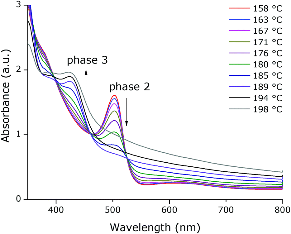 | ||
| Fig. 5 Absorption spectra as a function of temperature, between 158 °C and 198 °C, starting from a spin-coated film of (BTBT-C3)2PbI4 that was dried at 50 °C for 5 min before the in situ experiment. The black arrows indicate decreasing or increasing absorbance as a function of temperature. | ||
 | ||
| Fig. 6 Absorbance at 503 nm (red; following consecutively phase 1, phase 2 and PbI2) and at 424 nm (blue; following phase 3) as a function of temperature, extracted from the absorption spectra at different temperatures starting from a spin-coated film of (BTBT-C3)2PbI4 that was dried at 50 °C for 5 min before the in situ experiment. The increase in absorbance at 503 nm starting at ∼190 °C is due to the formation of lead iodide. | ||
T-XRD results are conform with the absorption spectra. At temperatures below ∼140 °C, a weakly crystalline phase is present (phase 1). Then a highly crystalline phase is formed (phase 2). This phase is present until ∼180 °C in this experiment when reflections of phase 3, corresponding to the excitonic peak at ∼424 nm from T-UVVIS, start to appear, as well as lead iodide with a main reflection at ∼12.5° (Fig. 7; the same plot with absolute intensities is shown in Fig. S4, ESI†).
 | ||
| Fig. 7 X-ray diffraction patterns (normalized) as a function of temperature starting from a spin-coated film of (BTBT-C3)2PbI4 that was dried at 50 °C for 5 min before the in situ experiment. The broad peak at ∼6.6° 2ϑ is due to Kapton from the temperature chamber of the XRD apparatus. | ||
Single-crystals of phase 3 were obtained using an anti-solvent vapour diffusion crystallization approach as detailed in the ESI† and their crystal structure was determined. The inorganic framework consists of a combination of face- and corner-sharing PbI64− octahedra (Fig. 8). The simulated XRD pattern for this crystal structure matches well with the experimental XRD pattern of a thin film of phase 3 (Fig. S5, ESI†). This hybrid does indeed possess an inorganic framework of a lower dimensionality than that of a 2D layered perovskite, confirming what could be expected based on the higher energy excitonic peak position.
 | ||
| Fig. 8 Unit cell of (BTBT-C3)4Pb3I10 (phase 3). The lead atoms are coloured bright grey, the iodine atoms dark purple, the nitrogen atoms light blue, the hydrogen atoms light pink, the carbon atoms dark orange and the sulphur atoms yellow. This figure was made using VESTA. | ||
Regrettably, we were unable up until now to obtain single-crystals of phase 2 (which we identify as the 2D layered perovskite phase based on excitonic peak position and the pattern of characteristic reflections in XRD) due to a strong tendency for crystals of phase 3 to form regardless of the supplied precursor stoichiometry. Next to the crystals of phase 3, crystals of a different hybrid containing gamma-butyrolactone (GBL) solvent molecules were obtained using an alternative crystal growth approach (as detailed in the ESI†). These crystals have an empirical formula of (BTBT-C3)PbI3·(GBL) and their inorganic framework consists of 1D ribbons of face-sharing octahedra (Fig. S6, ESI†). Since we did not employ GBL to prepare precursor solutions for spin-coating, this crystal phase is not present in our thin films.
Solvent vapour annealing
Since obtaining highly crystalline films of this material using regular thermal annealing showed to be difficult, presumably due to the relatively high molecular weight and the rigidity of the BTBT cation, we were interested in testing a combined thermal-solvent vapour annealing method.For this purpose, the high-boiling solvent DMSO (boiling point = 189 °C) was used and the procedure was carried out inside of a glovebox. The method used was adapted from ref. 26. A drop of DMSO was put on a hot plate (kept at the annealing temperature of the film), the spin-coated film was quickly put on the hot-plate next to this drop and a Petri dish was used to immediately cover both the film and the drop. The DMSO drop evaporates and generates an atmosphere containing DMSO for the film during annealing. We hypothesize that the presence of DMSO vapour during the annealing of the films creates enhanced mobility for the different components, thereby facilitating the structure formation. Since the BTBT derivative that we use is relatively bulky and very rigid due to its fused ring system, we expect that this component is the main cause for the difficulty to obtain fully formed films of the perovskite using a short thermal annealing procedure. From a literature survey, it is clear that fully formed 2D perovskite films can be obtained using low annealing temperatures (or even without an annealing step) when small flexible organic cations such as butylammonium are employed,41 while much higher annealing temperatures are necessary when higher molecular weight organic cations such as quaterthiophene derivatives are used.15,42 This could be related to the difference in mobility (i.e. the energy needed to reorganize) between these different organic cations.
The resulting absorption spectra of solvent vapour annealed films are shown in Fig. 9, compared to the absorption spectrum of a film thermally annealed at 150 °C (denoted NA; from Fig. 2). Since all of the absorption spectra in Fig. 2 are all nearly identical, the one for the film annealed at 150 °C was chosen here as a reference. As can be seen, for solvent vapour annealing (denoted SA) at 140 °C, 150 °C and 190 °C for 15 min, intense excitonic absorption peaks are obtained. Note that a certain threshold annealing temperature is still required for solvent vapour annealing since the samples annealed at temperatures below 140 °C for 15 min do not possess an intense excitonic absorption peak. Notice also that in the absorption spectra with the strong excitonic peaks (>140 °C), the shape of the absorption spectrum clearly changes around 315 nm. This region corresponds to the absorption of BTBT molecules (Fig. S7, ESI†). It is known in literature that the peaks in the absorption spectrum of BTBT organic small molecules shift and change in this wavelength region depending on the type of aggregation.43 Therefore, we hypothesize that this change in spectral shape could be an indication for a difference in the stacking (or the extent of ordering) of the BTBT molecules inside of the hybrid. For the film that was solvent vapour annealed at 190 °C, the shape in this region is different again. This could be related to the presence of more substantial amounts of phase 3 present in this film due to the degradation of the 2D hybrid (Fig. S8, ESI†).
 | ||
| Fig. 9 Absorption spectra of films of (BTBT-C3)2PbI4 that were solvent vapour annealed (SA) at different temperatures for 15 min compared to the thermally annealed sample (NA) at 150 °C. | ||
The XRD pattern of the film that was solvent vapour annealed at 150 °C for 15 min (Fig. 10) has very intense reflections, even relative to a pattern obtained from T-XRD where the total annealing time for the film is much longer (see ESI† for details on the T-XRD experiment). Note that all of our samples were prepared using spin-coating with the same spin settings and starting from a precursor solution with the same concentration. This suggests that the degree of crystallinity and/or the degree of orientation for this solvent annealed film is much higher than for the other samples. Note that there are reflections present in the pattern corresponding to phase 3 identified above using T-XRD and T-UVVIS. For the film that was thermally annealed at 150 °C for 15 minutes without solvent vapour annealing (from Fig. 3), the full width at half maximum (FWHM) of the first and second reflections in the pattern (respectively 0.26° and 0.25°) is significantly higher than for the first and second reflections (respectively 0.11° and 0.13°) in the pattern of the film that was solvent vapour annealed at 150 °C for 15 min (from Fig. 10). The FWHM for the reflections in the patterns for the other thermally annealed films are also significantly higher than for the equivalent solvent vapour annealed films. Combined with the significantly enhanced reflection intensity, the decrease in the FWHM of the reflections suggests the growth of a larger density of coherently scattering crystalline domains in the solvent vapour annealed films, resulting in enhanced overall crystallinity.44
 | ||
| Fig. 10 Comparison between the XRD patterns of (BTBT-C3)2PbI4 films subjected to different treatments. The blue pattern belongs to a film that was solvent vapour annealed (SA) at 150 °C for 15 min and the red pattern belongs to a film from T-XRD at 160 °C (from Fig. 9). | ||
As could be expected based on the absorption spectra and the XRD patterns, this solvent annealed film also possesses relatively strong excitonic emission (Fig. 11). Consistent with the absorption spectra (Fig. 9), the emission intensity of the films that were solvent annealed at 150 °C and 190 °C (giving rise to intense excitonic absorption peaks) is orders of magnitude higher than that of the film solvent annealed at 110 °C (not possessing the strong excitonic absorption peak). Likewise, the emission intensity for films obtained using regular thermal annealing, for the same annealing time, is orders of magnitude lower than for the film that was solvent annealed at 150 °C (Fig. S9–S11, ESI†). Moreover, in the emission spectra of the thermally annealed films, there is an additional weak emission feature at lower energies (higher wavelengths) than the exitonic emission peak. This could be related to the emission from defects present in these films,45 which would be consistent with the hypothesis that the 2D perovskite in these thermally annealed films is not fully formed. From SEM images, there is no significant difference in film morphology between films that were annealed using the regular thermal annealing and films that were solvent vapour annealed (Fig. S12, ESI†).
 | ||
| Fig. 11 Emission spectra of films of (BTBT-C3)2PbI4 that were solvent annealed for 15 min at different temperatures. The films were excited at 430 nm. | ||
Photoconductivity TRMC
In order to determine if the superior absorption characteristics and enhanced crystallinity of the films obtained using solvent vapour annealing translate into superior electronic transport properties, we measured the photoconductivity time-resolved microwave conductivity (TRMC) of solvent vapour-annealed films as well as of thermally annealed films. The photoconductivity TRMC measurements determine the product of the sum of mobility of charge carriers (∑μ) and yield of dissociation of charge carriers (φ) in semiconductor materials according to eqn (1).46 The yield of dissociation (φ) strongly depends on the exciton binding energy of the material studied. It is possible that photogenerated charge carriers (excitons) recombine during the pulse without contributing to the photoconductivity signal (response time of the microwave setup is ∼18 ns). | (1) |
 | ||
| Fig. 12 Photoconductivity TRMC of (BTBT-C3)2PbI4 thermal evaporated films (NA) and solvent vapour annealed films (SA). The films were excited at ∼490 nm with a photon intensity of 4.3 × 10¹² ph cm−2 (concentration of ∼1014 cm−3). | ||
Device characteristics
We wanted to verify if the higher photoconductivity of the solvent vapour annealed films measured using TRMC also results in superior device characteristics. Devices with a simple architecture were made, consisting of films deposited directly onto a quartz substrate with a gold electrode evaporated directly on top of the films. A mask was used for the deposition of the gold electrode such that interdigitating finger structures are obtained (Fig. S14, ESI†). In this way, a current is measured between these interdigitating fingers when a voltage is applied over them. Note that it is not the purpose of this preliminary study to obtain highly optimized optoelectronic devices. However, equivalent devices were prepared in duplicate using either regularly thermally annealed or solvent vapour annealed films. The devices were subjected to a light intensity of 1 sun with a spectrum of A.M. 1.5G (ASTM). The result is shown in Fig. 13 (in all cases for the cell with the largest spacing between the finger structures). It is clear that the light current density extracted at a certain applied voltage is significantly higher for the solvent vapour annealed films compared to the regular thermally annealed films. This indicates that the superior film characteristics do indeed result in enhanced optoelectronic characteristics, in this case, extracted light current density under applied voltage. The dark current density of the films was also measured. Compared to the dark current density, the light current density is a factor of ∼200–1000 higher (depending on the applied voltage between −10 V and +10 V) (Fig. S15 and S16, ESI†). The dark current density for the devices containing the solvent vapour annealed films is similar to that of devices containing the regularly annealed films (Fig. S17, ESI†).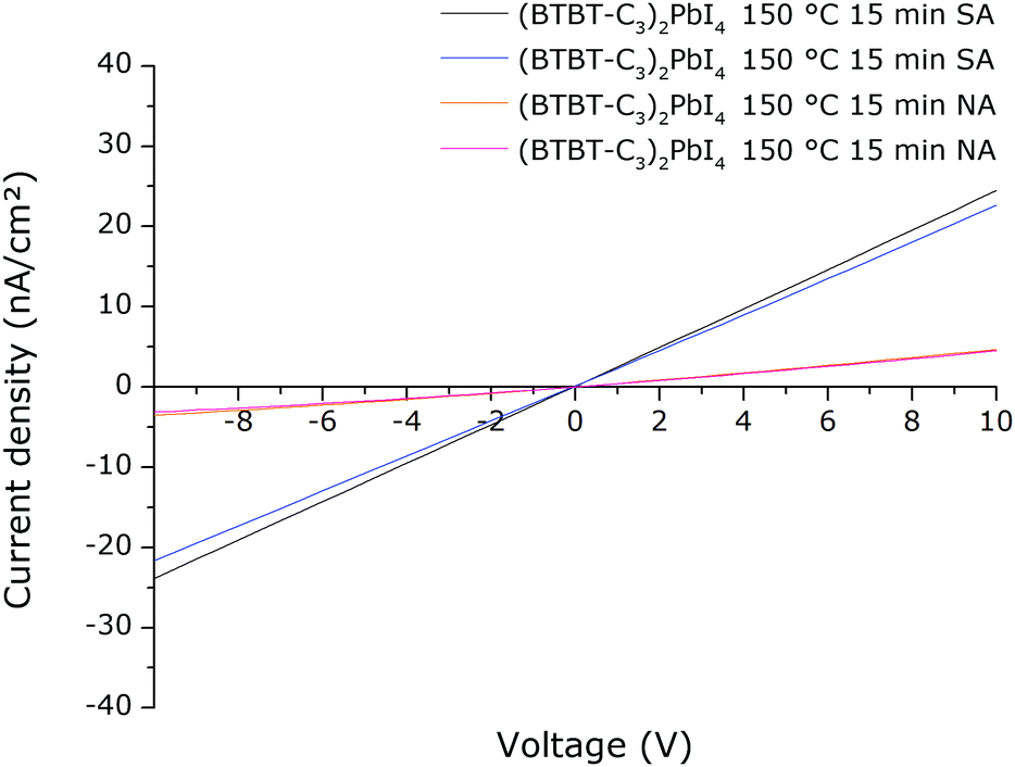 | ||
| Fig. 13 Current density–voltage (J–V) characteristics for four (BTBT-C3)2PbI4 devices, two of which contain a film that was not solvent vapour annealed (NA) and two of which contain a film that was solvent annealed (SA). | ||
In conclusion, the solvent vapour annealing method can significantly reduce the annealing temperature needed to obtain (BTBT-C3)2PbI4 films with enhanced absorption, emission, crystallinity, photoconductivity and light current density under an applied voltage.
Conclusions
A benzothieno[3,2-b]benzothiophene (BTBT) alkylammonium cation was incorporated into the organic layer of a 2D layered lead iodide perovskite. We show that the 2D layered hybrid degrades into a hybrid with an inorganic network of a lower dimensionality consisting of face- and corner-sharing PbI64− octahedra before further degradation of the material system into lead iodide. Using a mixed thermal/solvent vapour annealing approach, films of the 2D layered perovskite with enhanced absorption, emission and crystallinity were obtained. These solvent annealed films also possess enhanced photoconductivity in time-resolved microwave conductivity measurements and devices. Future work will be focussed on exploring the device physics of BTBT 2D layered perovskite-based optimized optoelectronic devices in detail. Furthermore, a computational study into the electronic structure of the 2D layered perovskite is foreseen when single crystals of this phase are obtained that allow determining its crystal structure.Conflicts of interest
There are no conflicts to declare.Acknowledgements
W. T. M. V. G., L. L. and D. V. acknowledge the FWO for the funding of the SBO project PROCEED (FWO-S002019N) and the senior FWO research project G043320N. M. M. is an SB PhD fellow at FWO (Number 1S20118N), R. H. is a PhD in chemistry currently employed as an R&D Project Leader at Agfa and P.-H. D. is a special research fund (BOF) doctoral (PhD) student at UHasselt/IMO. The research leading to these results in the Delft University of Technology has received funding from the European Research Council Horizon 2020 ERC Grant Agreement no. 648433. KVH thanks the Hercules Foundation (AUGE/11/029) and the Special Research Fund (BOF) – UGent (01N03217) for funding.References
- L. Mao, C. C. Stoumpos and M. G. Kanatzidis, J. Am. Chem. Soc., 2019, 141, 1171–1190 CrossRef CAS PubMed.
- G. Grancini and M. K. Nazeeruddin, Nat. Rev. Mater., 2018, 4, 4–22 CrossRef.
- H. Tsai, R. Asadpour, J. C. Blancon, C. C. Stoumpos, J. Even, P. M. Ajayan, M. G. Kanatzidis, M. A. Alam, A. D. Mohite and W. Nie, Nat. Commun., 2018, 9, 2130 CrossRef PubMed.
- W. T. M. Van Gompel, R. Herckens, K. Van Hecke, B. Ruttens, J. D'Haen, L. Lutsen and D. Vanderzande, Chem. Commun., 2019, 55, 2481–2484 RSC.
- H. Hu, F. Meier, D. Zhao, Y. Abe, Y. Gao, B. Chen, T. Salim, E. E. M. Chia, X. Qiao, C. Deibel and Y. M. Lam, Adv. Mater., 2018, 30, 1707621 CrossRef PubMed.
- M. D. Smith, B. A. Connor and H. I. Karunadasa, Chem. Rev., 2019, 119, 3104–3139 CrossRef CAS PubMed.
- J. V. Passarelli, D. J. Fairfield, N. A. Sather, M. P. Hendricks, H. Sai, C. L. Stern and S. I. Stupp, J. Am. Chem. Soc., 2018, 140, 7313–7323 CrossRef CAS PubMed.
- M. C. Gelvez-Rueda, W. T. M. Van Gompel, R. Herckens, L. Lutsen, D. Vanderzande and F. C. Grozema, J. Phys. Chem. Lett., 2020, 11, 824–830 CrossRef CAS PubMed.
- W. T. M. Van Gompel, R. Herckens, K. Van Hecke, B. Ruttens, J. D'Haen, L. Lutsen and D. Vanderzande, ChemNanoMat, 2019, 5, 323–327 CrossRef CAS.
- N. Marchal, W. Van Gompel, M. C. Gelvez-Rueda, K. Vandewal, K. Van Hecke, H. G. Boyen, B. Conings, R. Herckens, S. Maheshwar, L. Lutsen, C. Quarti, F. C. Grozema, D. Vanderzande and D. Beljonne, Chem. Mater., 2019, 31, 6880–6888 CrossRef CAS.
- R. Herckens, W. T. M. Van Gompel, W. Y. Song, M. C. Gelvez-Rueda, A. Maufort, B. Ruttens, J. D'Haen, F. C. Grozema, T. Aernouts, L. Lutsen and D. Vanderzande, J. Mater. Chem. A, 2018, 6, 22899–22908 RSC.
- W. A. Dunlap-Shohl, E. T. Barraza, A. Barrette, S. Dovletgeldi, G. Findik, D. J. Dirkes, C. Liu, M. K. Jana, V. Blum, W. You, K. Gundogdu, A. D. Stiff-Roberts and D. B. Mitzi, Mater. Horiz., 2019, 6, 1707–1716 RSC.
- C. Liu, W. Huhn, K. Z. Du, A. Vazquez-Mayagoitia, D. Dirkes, W. You, Y. Kanai, D. B. Mitzi and V. Blum, Phys. Rev. Lett., 2018, 121, 146401 CrossRef CAS PubMed.
- J. Leveillee, C. Katan, J. Even, D. Ghosh, W. Nie, A. D. Mohite, S. Tretiak, A. Schleife and A. J. Neukirch, Nano Lett., 2019, 19, 8732–8740 CrossRef CAS PubMed.
- Y. Gao, Z. Wei, P. Yoo, E. Shi, M. Zeller, C. Zhu, P. Liao and L. Dou, J. Am. Chem. Soc., 2019, 141, 15577–15585 CrossRef CAS PubMed.
- Y. Gao, E. Shi, S. Deng, S. B. Shiring, J. M. Snaider, C. Liang, B. Yuan, R. Song, S. M. Janke, A. Liebman-Pelaez, P. Yoo, M. Zeller, B. W. Boudouris, P. Liao, C. Zhu, V. Blum, Y. Yu, B. M. Savoie, L. Huang and L. Dou, Nat. Chem., 2019, 11, 1151–1157 CrossRef CAS PubMed.
- Z. Fang, M. Shang, Y. Zheng, T. Zhang, Z. Du, G. Wang, X. Duan, K.-C. Chou, C.-H. Lin, W. Yang, X. Hou and T. Wu, Mater. Horiz., 2020, 7, 1042–1050 RSC.
- S. Deng, J. M. Snaider, Y. Gao, E. Shi, L. Jin, R. D. Schaller, L. Dou and L. Huang, J. Chem. Phys., 2020, 152, 044711 CrossRef PubMed.
- C. Niebel, Y. Kim, C. Ruzié, J. Karpinska, B. Chattopadhyay, G. Schweicher, A. Richard, V. Lemaur, Y. Olivier, J. Cornil, A. R. Kennedy, Y. Diao, W.-Y. Lee, S. Mannsfeld, Z. Bao and Y. H. Geerts, J. Mater. Chem. C, 2015, 3, 674–685 RSC.
- K. Takimiya, I. Osaka, T. Mori and M. Nakano, Acc. Chem. Res., 2014, 47, 1493–1502 CrossRef CAS PubMed.
- Y. Tsutsui, G. Schweicher, B. Chattopadhyay, T. Sakurai, J. B. Arlin, C. Ruzie, A. Aliev, A. Ciesielski, S. Colella, A. R. Kennedy, V. Lemaur, Y. Olivier, R. Hadji, L. Sanguinet, F. Castet, S. Osella, D. Dudenko, D. Beljonne, J. Cornil, P. Samori, S. Seki and Y. H. Geerts, Adv. Mater., 2016, 28, 7106–7114 CrossRef CAS PubMed.
- R. Janneck, N. Pilet, S. P. Bommanaboyena, B. Watts, P. Heremans, J. Genoe and C. Rolin, Adv. Mater., 2017, 29, 1703864 CrossRef PubMed.
- D. B. Mitzi, J. Chem. Soc., Dalton Trans., 2001, 1–12 RSC.
- S. Maheshwari, T. J. Savenije, N. Renaud and F. C. Grozema, J. Phys. Chem. C, 2018, 122, 17118–17122 CrossRef CAS PubMed.
- W. A. Dunlap-Shohl, Y. Zhou, N. P. Padture and D. B. Mitzi, Chem. Rev., 2019, 119, 3193–3295 CrossRef CAS PubMed.
- Z. Xiao, Q. Dong, C. Bi, Y. Shao, Y. Yuan and J. Huang, Adv. Mater., 2014, 26, 6503–6509 CrossRef CAS PubMed.
- Y. Deng, E. Peng, Y. Shao, Z. Xiao, Q. Dong and J. Huang, Energy Environ. Sci., 2015, 8, 1544–1550 RSC.
- Q. Liang, J. Liu, Z. Cheng, Y. Li, L. Chen, R. Zhang, J. Zhang and Y. Han, J. Mater. Chem. A, 2016, 4, 223–232 RSC.
- L. Hu, G. Shao, T. Jiang, D. Li, X. Lv, H. Wang, X. Liu, H. Song, J. Tang and H. Liu, ACS Appl. Mater. Interfaces, 2015, 7, 25113–25120 CrossRef CAS PubMed.
- H. Yu, X. D. Liu, Y. J. Xia, Q. Q. Dong, K. C. Zhang, Z. W. Wang, Y. Zhou, B. Song and Y. F. Li, J. Mater. Chem. A, 2016, 4, 321–326 RSC.
- J. R. Lian, Q. Wang, Y. B. Yuan, Y. C. Shao and J. S. Huang, J. Mater. Chem. A, 2015, 3, 9146–9151 RSC.
- S. H. Chin, J. W. Choi, H. C. Woo, J. H. Kim, H. S. Lee and C. L. Lee, Nanoscale, 2019, 11, 5861–5867 RSC.
- D. Liang, Y. Peng, Y. Fu, M. J. Shearer, J. Zhang, J. Zhai, Y. Zhang, R. J. Hamers, T. L. Andrew and S. Jin, ACS Nano, 2016, 10, 6897–6904 CrossRef CAS PubMed.
- C. Ma, D. Shen, T. W. Ng, M. F. Lo and C. S. Lee, Adv. Mater., 2018, 30, 1800710 CrossRef PubMed.
- J. Qing, X. K. Liu, M. J. Li, F. Liu, Z. C. Yuan, E. Tiukalova, Z. B. Yan, M. Duchamp, S. Chen, Y. M. Wang, S. Bai, J. M. Liu, H. J. Snaith, C. S. Lee, T. C. Sum and F. Gao, Adv. Energy Mater., 2018, 8, 1800185 CrossRef.
- Z. H. Zheng, H. B. Lan, Z. H. Su, H. X. Peng, J. T. Luo, G. X. Liang and P. Fan, Sci. Rep., 2019, 9, 17422 CrossRef.
- G. C. Papavassiliou and I. B. Koutselas, Synth. Met., 1995, 71, 1713–1714 CrossRef CAS.
- G. C. Papavassiliou, G. A. Mousdis and I. B. Koutselas, Adv. Mater. Opt. Electron., 1999, 9, 265–271 CrossRef CAS.
- K. Pradeesh, K. N. Rao and G. V. Prakash, J. Appl. Phys., 2013, 113, 083523 CrossRef.
- K. Z. Du, Q. Tu, X. Zhang, Q. Han, J. Liu, S. Zauscher and D. B. Mitzi, Inorg. Chem., 2017, 56, 9291–9302 CrossRef CAS PubMed.
- D. H. Cao, C. C. Stoumpos, O. K. Farha, J. T. Hupp and M. G. Kanatzidis, J. Am. Chem. Soc., 2015, 137, 7843–7850 CrossRef CAS PubMed.
- D. B. Mitzi, K. Chondroudis and C. R. Kagan, Inorg. Chem., 1999, 38, 6246–6256 CrossRef CAS PubMed.
- V. S. Vyas, R. Gutzler, J. Nuss, K. Kern and B. V. Lotsch, CrystEngComm, 2014, 16, 7389–7392 RSC.
- C. M. M. Soe, W. Y. Nie, C. C. Stoumpos, H. Tsai, J. C. Blancon, F. Z. Liu, J. Even, T. J. Marks, A. D. Mohite and M. G. Kanatzidis, Adv. Energy Mater., 2018, 8, 1700979 CrossRef.
- G. Zhou, B. Su, J. Huang, Q. Zhang and Z. Xia, Mater. Sci. Eng., R, 2020, 141, 100548 CrossRef.
- T. J. Savenije, A. J. Ferguson, N. Kopidakis and G. Rumbles, J. Phys. Chem. C, 2013, 117, 24085–24103 CrossRef CAS.
- M. C. Gelvez-Rueda, E. M. Hutter, D. H. Cao, N. Renaud, C. C. Stoumpos, J. T. Hupp, T. J. Savenije, M. G. Kanatzidis and F. C. Grozema, J. Phys. Chem. C, 2017, 121, 26566–26574 CrossRef PubMed.
Footnote |
| † Electronic supplementary information (ESI) available: Details on the synthesis of the BTBT cation, thin film deposition and annealing, synthesis and characterization of single-crystals and measurement techniques. Supporting figures include an absorption spectrum, XRD pattern, unit cell, SEM images, photoconductivity transients and I–V curves. CCDC 1914880 and 1985268. For ESI and crystallographic data in CIF or other electronic format see DOI: 10.1039/d0tc01053g |
| This journal is © The Royal Society of Chemistry 2020 |