
 Open Access Article
 This Open Access Article is licensed under a
 Creative Commons Attribution 3.0 Unported Licence
A cryogenic solid-state reaction at the interface between Ti and the Bi2Se3 topological insulator
Katja
Ferfolja
 a,
Mattia
Fanetti
*a,
Sandra
Gardonio
a,
Mirco
Panighel
b,
Igor
Píš
bc,
Silvia
Nappini
b and
Matjaz
Valant
ad
a,
Mattia
Fanetti
*a,
Sandra
Gardonio
a,
Mirco
Panighel
b,
Igor
Píš
bc,
Silvia
Nappini
b and
Matjaz
Valant
ad
aMaterials Research Laboratory, University of Nova Gorica, Vipavska 11c, SI-5270 Ajdovščina, Slovenia. E-mail: mattia.fanetti@ung.si
bCNR-IOM, Istituto Officina dei Materiali, S.S. 14, km 163.5, I-34149 Trieste, Italy
cElettra-Sincrotrone Trieste S.C.p.A., S.S. 14, km 163.5, I-34149, Trieste, Italy
dInstitute of Fundamental and Frontier Sciences, University of Electronic Science and Technology of China, Chengdu 610054, China
First published on 20th July 2020
Abstract
Understanding the chemical processes at the interface between a metal and topological insulator (TI) is important when it comes to designing devices that exploit the peculiar topological surface states or studying the properties of TI heterostructures. In this paper we show that the interface between Ti and Bi2Se3 is unstable at RT and results in the formation of interfacial phases of titanium selenides and metallic Bi. The reaction has shown significant kinetics already at cryogenic temperatures, which is very surprising for a solid-state redox reaction. This can be explained with the possibility of electrons in the topological surface states playing a role in enhancing the Bi2Se3 surface reactivity due to the electron-bath effect. For the Ti coverage above 40 nm, the interfacial processes cause compressive stress that triggers the morphological change (buckling) of the deposited film. The observed interface reaction, with all of its consequences, has to be considered not only in the design of devices, where the Ti adhesion layer is often used for contacts, but also for possible engineering of 2D TI heterostructures.
Introduction
TIs have attracted a lot of attention from the scientific community during the last decade due to their intriguing properties. They are characterized by a finite bandgap in their bulk and gapless topological surface states (TSSs) that are spin-polarized Dirac states.1,2 In ordinary semiconductors, the surface states originate from the surface termination and are very sensitive to surface defects or contamination.3 In contrast, TIs possess TSSs that come from their characteristic bulk band structure. The TSSs are protected by the time-reversal symmetry, making them extremely robust to the surface deformations or impurities.The above-described properties make TIs potentially applicable in catalysis, spintronic devices and low power electronic devices.4 In the majority of the foreseen applications, an interface between a metal and the TI is expected; not only in the common case of electric contacts but also for other specific functionalities such as in heterogeneous catalysis5,6 or charge-to-spin conversion.7,8 Despite this, the understanding of the metal/TI interface stability and structure is still poor, even for the metals that are already widely used such as titanium.
One of the most studied TIs, due to its relatively large bandgap (0.3 eV), is Bi2Se3. It crystallizes in a rhombohedral crystal structure and is constructed from quintuple layers (QLs) bonded together by the weak van der Waals forces. Bi2Se3 and its analogue Bi2Te39 are frequently used as model materials for testing and exploring the TI properties since their electronic structure is characterized by a single Dirac cone at the Γ point.1,2
The most commonly employed electric contact in the TI-based devices is Au with an adhesive layer of Ti10–12 or Cr,13,14 but other metals such as Pd,15 Pt16 or Ag17 have also been used. The stability of the metal contacts has been taken for granted for a long time. Recently, the awareness about the effect of the interface processes on a device performance has increased.18
In this context, the occurrence of a chemical interaction at the metal/TI interface can be critical for two main reasons. First, the formation of new interfacial phases may affect the electronic properties (e.g. the capability to maintain the spin-momentum locking) and the type of the contact. Second, during the reaction, the QLs are consumed and the TI thickness can decrease below 6 QL. Below this threshold, the wave functions of the top- and bottom-surface states start to overlap and a hybridization gap opens at the Dirac point,19 resulting in the disappearance of TSSs. This fact is especially important for the thin-films or nanostructured devices based on TIs.
Walsh et al.20 published a systematic study of various metals on Bi2Se3. Among them, Au appeared to be the least reactive. No interfacial phases were found by TEM. Yet, a weak interaction with Bi2Se3 was later detected by photoemission spectroscopy (XPS) measurements.20,21 Surprisingly, despite its noble-metal character, Ag showed a considerable amount of reactivity with the Bi2Se3 surface. A redox solid-state reaction at room temperature (RT) was observed at the Ag/Bi2Se3 interface, which yielded AgSe2, AgBiSe2 and metallic Bi.22 In addition, chemical reactions at the metal/TI interface have been detected for Fe,20,23–26 Cr,20,27 Co, Ni,20 Mn and Cu.28
Interdiffusion of Cu into Bi2Te3 was observed by Kong et al.29 who studied how the orientation of Bi2Te3 influences the resistivity of Cu metal contact. To suppress the diffusion, a Ti barrier layer was deposited, which successfully prevented the migration of Cu into the substrate. Despite the reduced Cu diffusion, the contact resistivity did not improve, and in fact, it even increased. It has been suggested that this effect could be due to the reduction of some compounds at the interface. However, the research was performed on a μm scale, therefore, it was not possible to detect potential reactions occurring between the interfacial layers of Bi2Te3 and Ti. Finally, Cho et al.15 published that the use of a Ti or Cr adhesion layer for metal contacts on ultrathin Bi2Se3 made the contact resistance increase rapidly with time. Oxidation of the adhesion layer was suggested, but no data or discussion was reported. In summary, the understanding of the interactions of different metals with TIs is still incomplete. This is also applicable for the titanium/TI interfacial interaction, which has never been characterized until now.
Here we present a comprehensive investigation of the Ti/Bi2Se3 interface, focusing on the chemical interactions between the two phases. A solid-state redox reaction with significant kinetics at room temperature was observed at the interface yielding titanium selenides and metallic Bi. Moreover, the solid-state chemical interaction was detected even at the cryogenic temperature (130 K). This surprising interface instability suggests the active role of the TSS electrons in the TI surface reactivity. Because of the frequent use of the Ti adhesive layer in the metal contacts, this study provides valuable guidance for the electric contact design. This newly gained knowledge can also be applied for the synthesis of novel 2D heterostructures.
Experimental
Bi2Se3 single crystals were synthesized by the Bridgman method. High purity Bi (99.999%) and Se (≥99.999%) were mixed in a molar ratio of Bi![[thin space (1/6-em)]](https://www.rsc.org/images/entities/char_2009.gif) :Se = 2:3.3 and sealed in a quartz ampoule filled with argon.30 The ampoule was placed in a furnace and heated to 860 °C for 24 h. After that, the temperature was slowly lowered (2° h−1) to 650 °C. The ampoule was maintained at this temperature for 7 days and then cooled down to room temperature (RT).
:Se = 2:3.3 and sealed in a quartz ampoule filled with argon.30 The ampoule was placed in a furnace and heated to 860 °C for 24 h. After that, the temperature was slowly lowered (2° h−1) to 650 °C. The ampoule was maintained at this temperature for 7 days and then cooled down to room temperature (RT).
Scanning tunneling microscopy (STM) measurements were carried out in ultra-high vacuum (UHV) at RT using an Omicron VT-STM apparatus. The samples were prepared by cleaving in situ to prevent surface contamination. Low-energy electron diffraction (LEED) was used to monitor the surface crystal structure. In the same UHV chamber, Ti has been deposited using an e-beam evaporator at a rate of 0.1 Å min−1. The STM measurements were performed at a pressure of 2 × 10⁻¹⁰ mbar in constant current mode, with the applied bias referred to the sample and the image analysis was performed using the Gwyddion analysis software.31
The samples for the XPS measurements were prepared by cleaving in a UHV preparation chamber at a pressure of 5.7 × 10⁻¹⁰ mbar. Different Ti coverages were evaporated using the e-beam evaporator at a rate of 0.23 Å min−1. The evaporation rate was determined from the attenuation of the substrate photoemission signals. XPS measurements were carried out at the BACH beamline of Elettra synchrotron (Trieste, Italy) using a VG-Scienta R3000 hemispherical electron analyzer. The spectra were recorded at normal emission at a base pressure lower than 3.3 × 10⁻¹⁰ mbar. All measurements were carried out at a beam energy of 650 eV with a total energy resolution (electron spectrometer and monochromator) of 0.2 eV. The binding energy scale was calibrated using the Au 4f7/2 peak (84.0 eV) of a clean gold reference. Oxygen and carbon core levels were monitored during all stages of the experiment and no contamination was detected.
Fitting of the spectra was performed with KolXPD software.32 All spectra were fitted with the spin–orbit doublets using Doniach-Sunjic line shape convoluted with a Gaussian function and a Shirley-type background. Lorentzian width, branching ratio and spin–orbit splitting were determined from the clean surface and were kept constant throughout the fitting analysis, while the Gaussian width, intensity and energy position were allowed to vary. The asymmetry parameters for metallic components were fixed to a non-zero value.
For the preparation of a 20 nm thick film, the Bi2Se3 single crystals were cleaved by tape stripping in air immediately before the Ti deposition in a precision etching coating system (PECS, Gatan, Model 682). The deposition was performed in vacuum at RT and a base pressure of 10−5 mbar at a rate of 0.5 Å s−1. Then, the samples for transmission electron microscopy (TEM) imaging were prepared following the standard specimen preparation procedure for a thin film cross-section analysis. The TEM imaging was performed using a field-emission transmission electron microscope (JEOL JEM-2100F-UHR). The elemental composition was analyzed in the STEM mode using the attached energy dispersive X-ray (EDX) spectroscopy detector (Oxford X-Max80T).
The sample preparation for scanning electron microscopy (SEM) imaging was performed by cleaving and deposition of Ti in PECS apparatus as for TEM imaging. The SEM imaging was carried out using a field-emission SEM (JEOL JSM-7100F TTLs).
Results and discussion
The study of the growth mode and morphology of Ti on Bi2Se3 at ultra-low coverage has been performed by STM. At very low Ti coverage (0.03 Å) the Bi2Se3 surface exhibits some defects that are not present on the clean surface (see Fig. 1a and b). A majority of them are in the form of triangular depressions, while others appear as 2 Å high bright spots. The triangles can appear as a result of a surface or subsurface substitutional defect.33–36Fig. 1c shows that the further Ti deposition (0.2 Å) results in an island growth mode, where two types of islands with different sizes are distinguished: the big islands with a width in the range of 5 to 10 nm and the small 3 nm wide islands. Line-profiles over the islands are shown in Fig. 1f. The big islands, that show a flat top surface, have an apparent height of 8.2 Å and a narrow height distribution (SD 0.4 Å). The apparent height of the small islands is 7 Å (SD 1 Å). The bimodal island formation on TI was also reported for Fe,26,33 that has a strong interaction with the substrate, and Co adatoms.37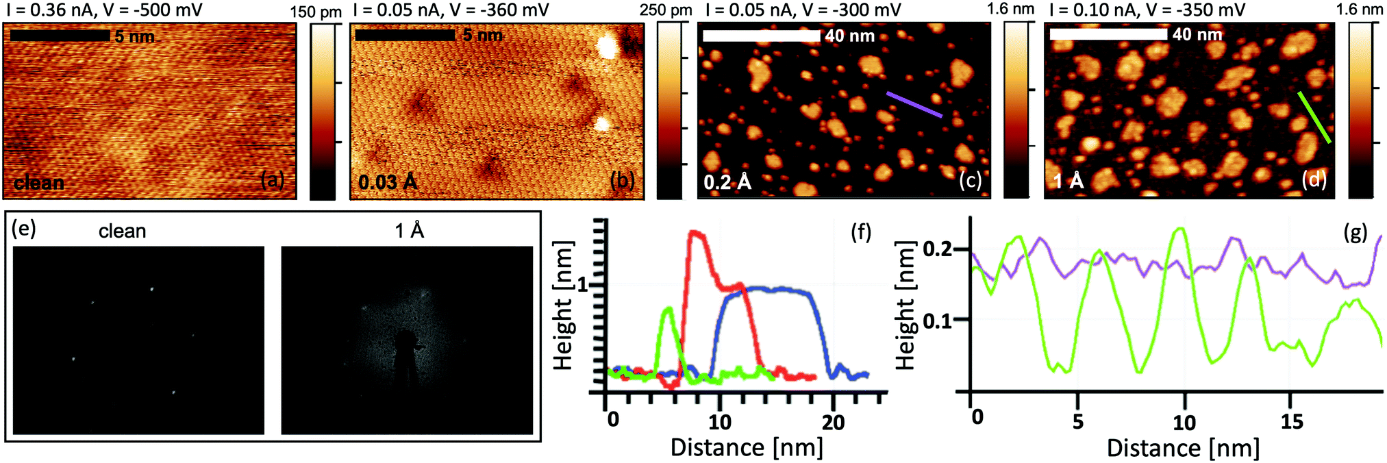 | ||
| Fig. 1 STM images of the clean substrate (a) and Ti/Bi2Se3 interface at the coverage of 0.03 Å (b), 0.2 Å (c) and 1 Å (d). (e) LEED pattern of the clean and Ti-covered Bi2Se3 surface. (f) Typical line profiles over the big islands (blue), small islands (green) and the island with an additional feature on the top (red). (g) Line profile over the substrate surface at coverages of 0.2 and 1 Å. Profiles correspond to the violet and green lines marked on images (c) and (d). | ||
At the Ti coverage of 1 Å the morphology of the Bi2Se3 substrate changes from smooth to coarse (Fig. 1d). The substrate exhibits pits that are approximately 1.5 Å deep and 2 nm wide as shown in the line profile in Fig. 1g. Accordingly, at that coverage, the LEED pattern of Bi2Se3 (Fig. 1e) is almost completely lost despite a significant part of the surface is still not covered by the islands. This indicates the loss of the crystallographic order in the Bi2Se3 substrate. The growth of the islands is strongly suppressed and with further Ti deposition the islands stop increasing in their lateral size. Instead, new features appear on the top of the already existing islands as shown in Fig. 1f with the red profile.
The chemical interaction at the Ti/Bi2Se3 interface was studied by XPS. The Bi 5d, Se 3d and Ti 2p core levels were measured for the nominal Ti coverage ranging from 0.5 to 28 Å. With the increase in the Ti coverage, the spectra shape changed significantly (Fig. 2), which indicates the strong chemical interaction at the interface. The observed changes indicate the change in the valence states and formation of new interfacial phases. A more detailed analysis of the XPS spectra was performed to reveal the full chemistry of the interaction.
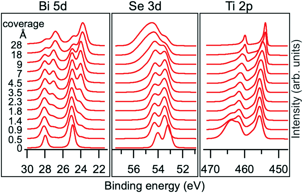 | ||
| Fig. 2 Evolution of Bi 5d, Se 3d and Ti 2p core level spectra with increasing Ti deposition on Bi2Se3. The spectra were normalized to the highest peak. | ||
The Bi 5d and Se 3d core levels of the clean Bi2Se3 surface are deconvoluted with one spin–orbit doublet. The corresponding peaks are positioned at BEs of 24.7 and 53.2 eV, respectively (see Fig. 3a) and are hereafter named Bi1 and Se1.
 | ||
| Fig. 3 Bi 5d and Se 3d core level spectra of the Ti/Bi2Se3 samples at different coverages: (a and b) pristine Bi2Se3; (c and d) 1.4 Å of Ti; and (e and f) 7 Å of Ti. | ||
A shift of 0.25 eV towards a higher BE is observed for the Se1 and Bi1 components (see Fig. 2) starting from the lowest Ti coverage (0.5 Å) and it is ascribed to the band bending. Upon Ti deposition, new components emerge in Se 3d and Bi 5d core levels (Se2 and Bi2, represented as blue components in Fig. 3), indicating a chemical reaction at the interface. The Se2 component has a 0.5 eV higher BE than Se1, whereas the Bi2 component is at 1.1 eV lower BE than Bi1 and fits well with the peak position of metallic Bi.38
With the increase in the Ti coverage, the Bi1 component, corresponding to Bi3+ in Bi2Se3, decreases because of higher Ti coverage and formation of new surface phases. The Se1 component decreases much slower in its spectral weight than Bi1. This is in line with the fact that the BE of Se1 corresponds not only to Se2− from Bi2Se3 but also to the newly formed TiSe2.39–42 The position of the Se2 component corresponds to non-stoichiometric intermediate metal selenides,42,43 formed during the ongoing reaction.
The same interfacial chemical process also reflects in the evolution of Ti 2p core level spectra. Upon a low Ti-deposition coverage of 1.4 Å, the Ti 2p core level spectra display two components, Ti1 and Ti2, at 455.5 and 457 eV BE, respectively (Fig. 4a). The peak position of Ti1 components is in good agreement with the reported data for TiSe2,39,40,42,44 which is considered as a product of the reaction between Bi2Se3 and Ti. The Ti2 component (together with Se2) is ascribed to the TiSe2-based intermediate phase with an under-stoichiometric Se content.45
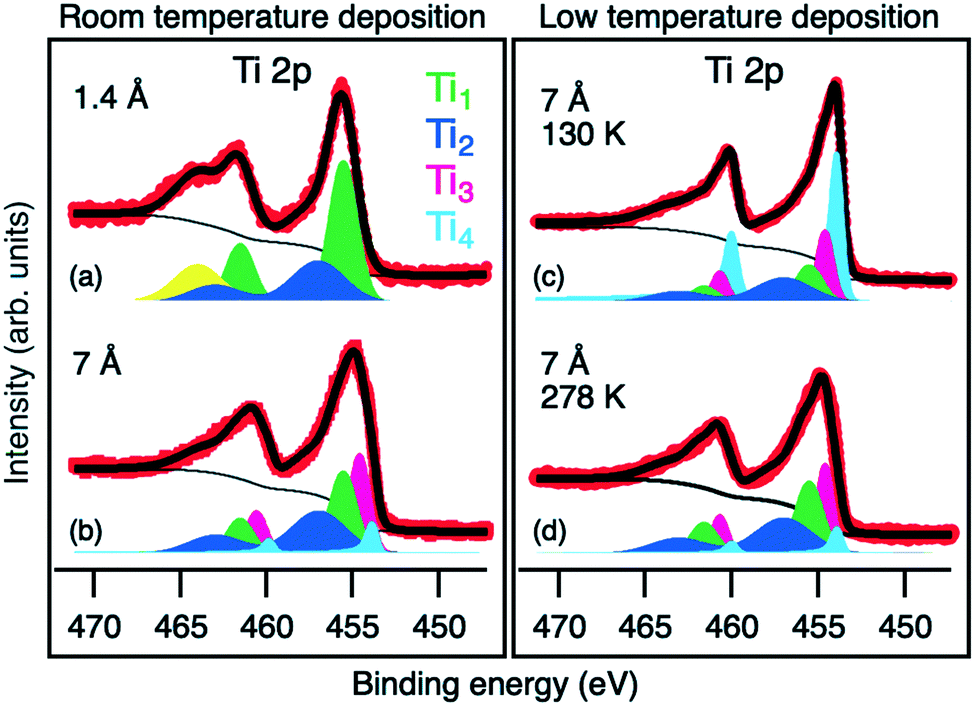 | ||
| Fig. 4 Ti 2p core level spectra of Bi2Se3 with deposited 1.4 Å of Ti at RT (a), 7 Å of Ti at RT (b) and 7 Å of Ti at 130 K (c). (d) Ti 2p core level spectrum obtained for the sample (c) after heating to 278 K. The yellow component corresponds to the Bi 4d3/2 core level peak, the red points are experimental data and the black solid line is the fit. | ||
After deposition of more than 4.5 Å of Ti, a new reaction regime is reached where new components emerge in all measured core levels. In the Ti 2p core level spectra, a Ti3 component at BE of 454.6 eV appears (pink colored in Fig. 4b). Its BE is between that of Ti0 and Ti4+ and can be attributed to Ti2+ due to the formation of TiSe. The corresponding Se component of TiSe is Se3 at a BE of 54.7 eV (pink colored in Fig. 3f).43
Due to the presence of the interfacial phases acting as the diffusion barrier, the deposited Ti is not completely consumed in the reaction and some of it remains in the metallic form. Ti0 corresponds to the Ti4 component at BE of 453.8 eV (light blue in Fig. 4), which becomes dominant above the 18 Å coverage (Fig. 2). In the Bi 5d core level, the new Bi3 component (pink colored in Fig. 3e) appears at 0.3 eV lower BE than Bi2. It is ascribed to metallic Bi46,47 with a different chemical environment, possibly due to alloying with Ti.
In summary, based on the presented analyses, we can claim that the Ti/Bi2Se3 interface is chemically unstable. The observed chemical interaction at the interface is a redox solid-state reaction that is kinetically active already at room temperature. Ion diffusion is the main parameter that influences the kinetics of such types of reactions. The kinetics slow down with an increase in the diffusion path through the product layer. Therefore, the appearance of the intermediate phases (such as TiSe and under-stoichiometric TiSe2) is expected. The interfacial reaction yields TiSe2 and metallic Bi as the final products of the solid-state redox reaction according to the equation:
| 3Ti + 2Bi2Se3 → 4Bi + 3TiSe2 |
During the reaction, Se remains in the −2 oxidation state, whereas the redox reaction happens between Bi3+ and Ti0 producing metallic Bi and Ti4+ compounds. The observed solid-state reaction is thermodynamically favored at room temperature (ΔG298 = −274 kJ mol−1 Ti).45,48 Within the same XPS experimental setup, the Ti deposition and measurement on the Bi2Se3 surface were additionally performed at a temperature of 130 K. The corresponding Ti 2p core level spectrum is shown in Fig. 4c. Surprisingly, the presence of the same reaction components Ti1, Ti2 and Ti3 as for the RT deposition (but with lower relative intensities) is observed again, which shows a significant reaction kinetics and a remarkable reactivity at the interface already at this cryogenic temperature. Heating the system up to RT enhances the reaction kinetics, resulting in the same XPS spectrum as observed for the RT deposition (see Fig. 4d).
The occurrence of the solid-state reaction, with significant kinetics already at a temperature as low as 130 K, raises the question on the origin of such marked reactivity of the Bi2Se3 surface. The reactivity is high despite the surface of Bi2Se3 does not display dangling bonds or unsaturated orbitals and it has been observed to be almost inert toward water, oxygen,49 CO and CO2.21 In a previous study we showed that TIs have the power to oxidize even noble metal atoms already at RT (Ag, see ref. 22), which is quite unusual and suggests the presence of a catalytic effect within the studied system. Our hypothesis is that the TSS electrons participate in the reaction by catalyzing it. As proposed by Chen et al.5 the electrons in the TSS can freely move over the surface, participate in hybridization and act as an effective electron bath. Their delocalization enables the migration of electrons from TIs to the adsorbates or vice versa5 enabling their participation in both oxidation and reduction processes.
To investigate the chemical reactivity at the Ti/Bi2Se3 interface under conditions more similar to the typical deposition of metals for applications (e.g. the deposition of Ti as an adhesive layer for electrodes), TEM analysis at the interface cross-section was performed on a sample with 20 nm of Ti deposited on Bi2Se3 at a rate of 0.6 Å s−1 by sputtering (Fig. 5a). In Fig. 5b the interplanar distance of 0.95 nm corresponds to the quintuple layers of Bi2Se3. At the interface between the substrate and the polycrystalline Ti film an interfacial layer with a crystal structure different from Bi2Se3 is observed. Within this layer, the darker area denotes the presence of heavier elements. Beside the darker region there is another interface phase with small domains and a layered structure (see Fig. 5c). The distance between these layers is about 0.60 nm, which fits well with a TiSe2(100) interplanar distance of 5.995 Å.44,50 The thickness of the overall interface region is approximately 10 nm.
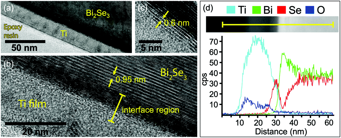 | ||
| Fig. 5 TEM image of the Ti/Bi2Se3 interface at lower magnification (a) and at high resolution (b). (c) TiSe2 layers beside the darker Bi region. (d) EDX line-scan over the interface region of the Ti/Bi2Se3 sample. | ||
An EDX line-scan over the interface is shown in Fig. 5d together with a dark field STEM image of the area of interest. On the left side, there is the unreacted Ti film (Ti EDX intensity profile is light blue). Deeper in the Ti film (from left to right), the first interfacial region with a thickness of 5 nm is Ti- and Se-rich with no Bi. This region is recognized as the titanium selenide phase. Further on, the second interfacial region contains almost only Bi, with the signals for Ti and Se reduced to extremely low intensity. Therefore, this region is ascribed to the metallic Bi, possibly with residual of Se and alloyed Ti. Deeper in the sample, the Bi and Se signals correspond to the bulk Bi2Se3. The observed structure of the interface with the presence of Ti selenide and metallic Bi is in agreement with the XPS observations.
The SEM analysis of the film morphology shows that up to 20 nm coverage, Ti produces a flat film over the whole surface of Bi2Se3 without visible features in the SEM images (Fig. 6a). No change in the surface morphology can be observed even after the sample being kept under ambient conditions for a month. This indicates that, after the formation of the interfacial phases, the reaction stops, contrary to what happens for Ag.22 However, the observed chemical interaction has dramatic macroscopic consequences when the Ti coverage increases to a certain threshold. At higher coverage (40 nm), the surface develops a network of hollow buckles of different mesh sizes as shown in Fig. 6b–e. The networks with bigger mesh sizes have 1.5 μm wide buckles whereas the buckles of more dense networks with smaller mesh sizes are about 0.35 μm wide. Such a structure is ascribed to the buckle delamination phenomenon. It shows typical morphological features such as network-like telephone cords where telephone cord blisters propagate on the undulating edges.51
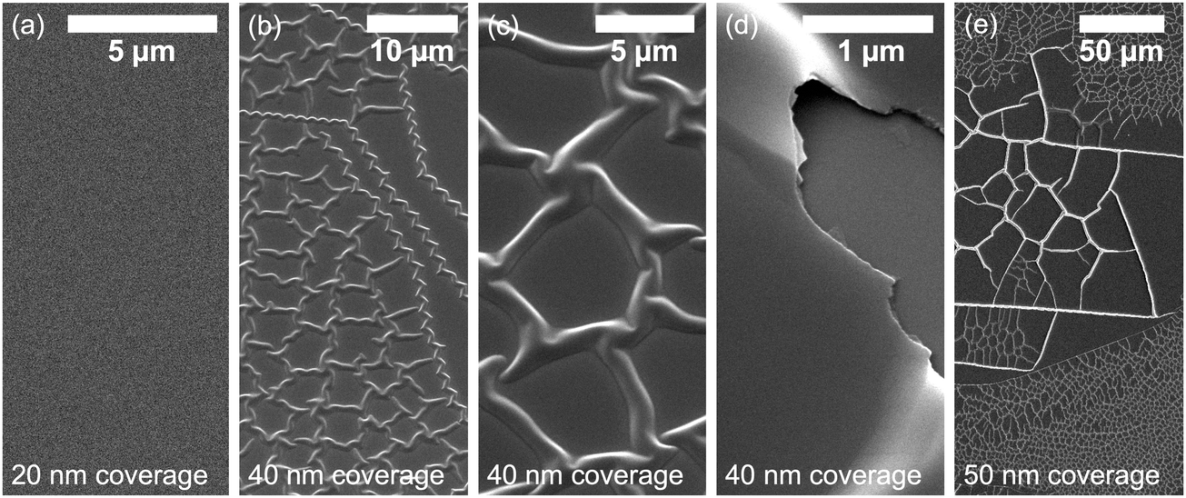 | ||
| Fig. 6 Morphology of the Ti film on Bi2Se3 at a nominal coverage of 20 nm (a) and 40 nm (b) by SEM. (c) Close-up images of the ripples. (d) Broken ripple showing the hollow inner part. (e) Image of the Ti film at lower magnification showing different morphologies of the ripples. | ||
Typically, such a morphology is observed after the release of compressive stress in the hard layer on a soft substrate.52 With the increasing coverage, the compressive stress is building up in the Ti polycrystalline film. In addition, a volumetric change created by the new phase is expected to generate additional compressive stress, since the Se atoms are absorbed into the Ti film. Finally, the formation of the metallic Bi phase, prone to plastic deformation, allows for sliding of the film. When the compressive stress overcomes the adhesive strength, the buckling occurs. The flat surface becomes unstable and stress is released by the formation of a spinodal-like pattern of wrinkles or buckles.53–55
To prove that the compressive stress is not generated by the oxidation of Ti after exposure to air, in a second experiment, immediately after the deposition of a 40 nm thick Ti film, a protective layer of Pt (10 nm) was deposited atop within the same apparatus. The sample exhibited the same morphology as that without the Pt layer, ruling out the possibility that the oxidation process is responsible for the buckling.
Conclusion
We have shown that the interface between Ti and Bi2Se3 is highly unstable at room temperature and produces an interface region containing titanium selenides and metallic Bi. Additionally, at high coverage (40 nm) buckle delamination of the Ti film occurs. These results should be considered whenever Ti is used in TI-based applications (e.g. as an adhesive layer in metal contacts), since the resulting interface structure may strongly affect the electronic (e.g. spin-momentum locking, Schottky barrier), transport and mechanical properties.The solid-state redox reaction has been detected with significant kinetics also at extraordinary low temperatures, as low as 130 K. The reported unquenched chemical reactivity at low temperature could be explained by considering the catalyzing role of the TSS in the electron transfer between the metal and TI as predicted by the theory.5,6,56
Even though more research is needed to fully understand the role of TSS electrons in the chemical reaction mechanisms, the high interface instability could in future be exploited for the synthesis of 2D metal selenides or for the study of heterostructures with Bi2Se3.
Conflicts of interest
There are no conflicts to declare.Acknowledgements
The work was financially supported by the Slovenian Research Agency, research core funding No. P2-0412. This project has received funding from the EU-H2020 research and innovation programme under grant agreement No. 654360 having benefitted from the access provided by IOM-CNR in Trieste (Italy) within the framework of the NFFA-Europe Transnational Access Activity. We thank Federica Bondino, Elena Magnano and Federico Salvador of BACH beamline@ELETTRA (IOM-CNR) and the staff of Variable and Low Temperature Scanning Tunneling Microscopy Laboratory (IOM-CNR) for the kind support.References
- C. L. Kane and E. J. Mele, Phys. Rev. Lett., 2005, 95, 146802 CrossRef CAS PubMed.
- L. Fu and C. L. Kane, Phys. Rev. B, 2007, 76, 045302 CrossRef.
- H. Lüth, Surfaces and Interfaces of Solid Materials, Springer, Berlin, 3rd edn, 1995 Search PubMed.
- D. S. Kong and Y. Cui, Nat. Chem., 2011, 3, 845–849 CrossRef CAS PubMed.
- H. Chen, W. G. Zhu, D. Xiao and Z. Y. Zhang, Phys. Rev. Lett., 2011, 107, 056804 CrossRef PubMed.
- J. P. Xiao, L. Z. Kou, C. Y. Yam, T. Frauenheim and B. H. Yan, ACS Catal., 2015, 5, 7063–7067 CrossRef CAS.
- S. Y. Shi, A. Z. Wang, Y. Wang, R. Ramaswamy, L. Shen, J. Moon, D. P. Zhu, J. W. Yu, S. Oh, Y. P. Feng and H. Yang, Phys. Rev. B, 2018, 97, 041115 CrossRef CAS.
- R. Sun, S. J. Yang, X. Yang, E. Vetter, D. L. Sun, N. Li, L. Su, Y. Li, Z. Z. Gong, Z. K. Xie, K. Y. Hou, Q. Gul, W. He, X. Q. Zhang and Z. H. Cheng, Nano Lett., 2019, 19, 4420–4426 CrossRef CAS PubMed.
- H. J. Zhang, C. X. Liu, X. L. Qi, X. Dai, Z. Fang and S. C. Zhang, Nat. Phys., 2009, 5, 438–442 Search PubMed.
- K. Zheng, L. B. Luo, T. F. Zhang, Y. H. Liu, Y. Q. Yu, R. Lu, H. L. Qiu, Z. J. Li and J. C. A. Huang, J. Mater. Chem. C, 2015, 3, 9154–9160 RSC.
- J. L. Yu, X. L. Zeng, L. G. Zhang, C. M. Yin, Y. H. Chen, Y. Liu, S. Y. Cheng, Y. F. Lai, K. He and Q. K. Xue, Opt. Express, 2018, 26, 4832–4841 CrossRef CAS PubMed.
- D. S. Kong, J. J. Cha, K. J. Lai, H. L. Peng, J. G. Analytis, S. Meister, Y. L. Chen, H. J. Zhang, I. R. Fisher, Z. X. Shen and Y. Cui, ACS Nano, 2011, 5, 4698–4703 CrossRef CAS PubMed.
- H. L. Peng, W. H. Dang, J. Cao, Y. L. Chen, W. Wu, W. S. Zheng, H. Li, Z. X. Shen and Z. F. Liu, Nat. Chem., 2012, 4, 281–286 CrossRef CAS PubMed.
- C. Ojeda-Aristizabal, M. S. Fuhrer, N. P. Butch, J. Paglione and I. Appelbaum, Appl. Phys. Lett., 2012, 101, 023102 CrossRef.
- S. J. Cho, N. P. Butch, J. Paglione and M. S. Fuhrer, Nano Lett., 2011, 11, 1925–1927 CrossRef CAS PubMed.
- A. A. Druzhinin, N. S. Liakh-Kaguy, I. P. Ostrovskii, Y. M. Khoverko and K. Rogacki, J. Nano- Electron. Phys., 2017, 9, 05013 Search PubMed.
- S. A. Ahmed and S. H. Mohamed, J. Mater. Sci., 2009, 44, 3043–3048 CrossRef CAS.
- A. Politano, M. S. Vitiello, L. Viti, D. W. Boukhvalov and G. Chiarello, FlatChem, 2017, 1, 60–64 CrossRef CAS.
- Y. Zhang, K. He, C. Z. Chang, C. L. Song, L. L. Wang, X. Chen, J. F. Jia, Z. Fang, X. Dai, W. Y. Shan, S. Q. Shen, Q. A. Niu, X. L. Qi, S. C. Zhang, X. C. Ma and Q. K. Xue, Nat. Phys., 2010, 6, 584–588 Search PubMed.
- L. A. Walsh, C. M. Smyth, A. T. Barton, Q. X. Wang, Z. F. Che, R. Y. Yue, J. Kim, M. J. Kim, R. M. Wallace and C. L. Hinkle, J. Phys. Chem. C, 2017, 121, 23551–23563 CrossRef CAS.
- M. Fanetti, I. Mikulska, K. Ferfolja, P. Moras, P. M. Sheverdyaeva, M. Panighel, A. Lodi-Rizzini, I. Pis, S. Nappini, M. Valant and S. Gardonio, Appl. Surf. Sci., 2019, 471, 753–758 CrossRef CAS.
- K. Ferfolja, M. Valant, I. Mikulska, S. Gardonio and M. Fanetti, J. Phys. Chem. C, 2018, 122, 9980–9984 CrossRef CAS.
- M. R. Scholz, J. Sanchez-Barriga, D. Marchenko, A. Varykhalov, A. Volykhov, L. V. Yashina and O. Rader, Phys. Rev. Lett., 2012, 108, 256810 CrossRef CAS PubMed.
- S. Majumder, K. Jarvis, S. K. Banerjee and K. L. Kavanagh, J. Vac. Sci. Technol., B: Nanotechnol. Microelectron.: Mater., Process., Meas., Phenom., 2017, 35, 04f105 Search PubMed.
- A. Polyakov, H. L. Meyerheim, E. D. Crozier, R. A. Gordon, K. Mohseni, S. Roy, A. Ernst, M. G. Vergniory, X. Zubizarreta, M. M. Otrokov, E. V. Chulkov and J. Kirschner, Phys. Rev. B: Condens. Matter Mater. Phys., 2015, 92, 045423 CrossRef.
- I. Vobornik, G. Panaccione, J. Fujii, Z. H. Zhu, F. Offi, B. R. Salles, F. Borgatti, P. Torelli, J. P. Rueff, D. Ceolin, A. Artioli, M. Unnikrishnan, G. Levy, M. Marangolo, M. Eddrief, D. Krizmancic, H. W. Ji, A. Damascelli, G. van der Laan, R. G. Egdell and R. J. Cava, J. Phys. Chem. C, 2014, 118, 12333–12339 CrossRef CAS.
- T. Yilmaz, W. Hines, F. C. Sun, I. Pletikosic, J. Budnick, T. Valla and B. Sinkovic, Appl. Surf. Sci., 2017, 407, 371–378 CrossRef CAS.
- H. J. Noh, J. Jeong, E. J. Cho, J. Park, J. S. Kim, I. Kim, B. G. Park and H. D. Kim, Phys. Rev. B: Condens. Matter Mater. Phys., 2015, 91, 121110 CrossRef.
- X. X. Kong, W. Zhu, L. L. Cao, Y. C. Peng, S. F. Shen and Y. Deng, ACS Appl. Mater. Interfaces, 2017, 9, 25606–25614 CrossRef CAS PubMed.
- M. Bianchi, R. C. Hatch, D. D. Guan, T. Planke, J. L. Mi, B. B. Iversen and P. Hofmann, Semicond. Sci. Technol., 2012, 27, 124001 CrossRef.
- D. Necas and P. Klapetek, Cent. Eur. J. Phys., 2012, 10, 181–188 Search PubMed.
- KolXPD, version 1.8.0 (build 61); software for spectroscopy data measurement and processing; https://www.kolibrik.net/kolxpd/, (accessed October 2019).
- T. Schlenk, M. Bianchi, M. Koleini, A. Eich, O. Pietzsch, T. O. Wehling, T. Frauenheim, A. Balatsky, J. L. Mi, B. B. Iversen, J. Wiebe, A. A. Khajetoorians, P. Hofmann and R. Wiesendanger, Phys. Rev. Lett., 2013, 110, 126804 CrossRef CAS PubMed.
- L. B. Abdalla, L. Seixas, T. M. Schmidt, R. H. Miwa and A. Fazzio, Phys. Rev. B: Condens. Matter Mater. Phys., 2013, 88, 045312 CrossRef.
- J. Kim, E. H. Shin, M. K. Sharma, K. Ihm, O. Dugerjav, C. Hwang, H. Lee, K. T. Ko, J. H. Park, M. Kim, H. Kim and M. H. Jung, Sci. Rep., 2019, 9, 1331 CrossRef PubMed.
- C. L. Song, Y. P. Jiang, Y. L. Wang, Z. Li, L. L. Wang, K. He, X. Chen, X. C. Ma and Q. K. Xue, Phys. Rev. B: Condens. Matter Mater. Phys., 2012, 86, 045441 CrossRef.
- M. Ye, S. V. Eremeev, K. Kuroda, E. E. Krasovskii, E. V. Chulkov, Y. Takeda, Y. Saitoh, K. Okamoto, S. Y. Zhu, K. Miyamoto, M. Arita, M. Nakatake, T. Okuda, Y. Ueda, K. Shimada, H. Namatame, M. Taniguchi and A. Kimura, Phys. Rev. B: Condens. Matter Mater. Phys., 2012, 85, 205317 CrossRef.
- J. C. Fuggle and N. Martensson, J. Electron Spectrosc. Relat. Phenom., 1980, 21, 275–281 CrossRef CAS.
- L. F. Sun, C. H. Chen, Q. H. Zhang, C. Sohrt, T. Q. Zhao, G. C. Xu, J. H. Wang, D. Wang, K. Rossnagel, L. Gu, C. G. Tao and L. Y. Jiao, Angew. Chem., Int. Ed., 2017, 56, 8981–8985 CrossRef CAS PubMed.
- S. Negishi, H. Negishi, K. Shimada, X. Y. Cui, M. Higashiguchi, M. Nakatake, M. Arita, H. Namatame, M. Taniguchi, A. Ohnishi and M. Sasaki, Phys. B, 2006, 383, 155–157 CrossRef CAS.
- W. Jaegermann, C. Pettenkofer, A. Schellenberger, C. A. Papageorgopoulos, M. Kamaratos, D. Vlachos and Y. Tomm, Chem. Phys. Lett., 1994, 221, 441–446 CrossRef CAS.
- A. S. Shkvarin, Y. M. Yarmoshenko, A. I. Merentsov, I. Pis, F. Bondino, E. G. Shkvarina and A. N. Titov, Inorg. Chem., 2018, 57, 5544–5553 CrossRef CAS PubMed.
- NIST X-Ray Photoelectron Spectroscopy Database, Version 4.1; National Institute of Standards and Technology: Gaithersburg, 2012, http://srdata.nist.gov/xps/, accessed November 2019.
- A. S. Shkvarin, Y. M. Yarmoshenko, N. A. Skorikov, M. V. Yablonskikh, A. I. Merentsov, E. G. Shkvarina and A. N. Titov, J. Exp. Theor. Phys., 2012, 114, 150–156 CrossRef CAS.
- L. N. Zelenina, T. P. Chusova and A. N. Titov, Russ. Chem. Bull., 2011, 60, 581–584 CrossRef CAS.
- T. Conard, R. Sporken, J. Ghijsen, L. M. Yu, R. Caudano, R. Seemann and R. L. Johnson, Surf. Sci., 1996, 369, 177–184 CrossRef CAS.
- A. Ettema and C. Haas, J. Phys.: Condens. Matter, 1993, 5, 3817–3826 CrossRef CAS.
- M. M. Binnewies and E. Milke, Thermochemical data of elements and compounds, Wiley-VCH Verlag GmbH, Weinheim, 2nd Revised and Extended edn, 2002 Search PubMed.
- L. V. Yashina, J. Sanchez-Barriga, M. R. Scholz, A. A. Volykhov, A. P. Sirotina, S. N. Vera, M. E. Tamm, A. Varykhalov, D. Marchenko, G. Springholz, G. Bauer, A. Knop-Gericke and O. Rader, ACS Nano, 2013, 7, 5181–5191 CrossRef CAS PubMed.
- P. Chen, Y. H. Chan, X. Y. Fang, S. K. Mo, Z. Hussain, A. V. Fedorov, M. Y. Chou and T. C. Chiang, Sci. Rep., 2016, 6, 37910 CrossRef CAS PubMed.
- Y. Ni and A. K. Soh, Acta Mater., 2014, 69, 37–46 CrossRef CAS.
- G. Abadias, E. Chason, J. Keckes, M. Sebastiani, G. B. Thompson, E. Barthel, G. L. Doll, C. E. Murray, C. H. Stoessel and L. Martinu, J. Vac. Sci. Technol., A, 2018, 36, 020801 CrossRef.
- J. Y. Faou, G. Parry, S. Grachev and E. Barthel, Phys. Rev. Lett., 2012, 108, 116102 CrossRef PubMed.
- M. J. Cordill and A. A. Taylor, Thin Solid Films, 2015, 589, 209–214 CrossRef CAS.
- M. Valant, M. Fanetti and U. Luin, Appl. Phys. Lett., 2016, 108, 151601 CrossRef.
- Q. L. He, Y. H. Lai, Y. Lu, K. T. Law and I. K. Sou, Sci. Rep., 2013, 3, 2497 CrossRef PubMed.
| This journal is © The Royal Society of Chemistry 2020 |