
 Open Access Article
 This Open Access Article is licensed under a
 Creative Commons Attribution 3.0 Unported Licence
A novel precursor towards buffer layer materials: the first solution based CVD of zinc oxysulfide†
Malavika A.
Bhide
 ,
Claire J.
Carmalt
and
Caroline E.
Knapp
*
,
Claire J.
Carmalt
and
Caroline E.
Knapp
*
Materials Chemistry Centre, Department of Chemistry, University College London, 20 Gordon Street, London WC1H 0AJ, UK. E-mail: caroline.knapp@ucl.ac.uk
First published on 19th March 2020
Abstract
We report the first solution based deposition of zinc oxysulfide, Zn(O,S), thin films via aerosol-assisted chemical vapour deposition (AACVD) facilitated by the use of a specifically designed precursor: [Zn8(SOCCH3)12S2] (1). This buffer layer material, synthesised from the dual source AACVD reaction of 1 with ZnEt2 and MeOH was analysed via X-ray diffraction (XRD), X-ray photoelectron spectroscopy (XPS), energy dispersive X-ray (EDX) analysis, scanning electron microscopy (SEM), Hall effect measurements and UV/vis spectroscopy. The film was highly transparent (>90%), conductive (ρ = 0.02998 Ω cm) and had a high charge carrier concentration (1.36 × 1019 cm−3), making it a good contendor as a buffer layer in thin film photovoltaics. In an additional study, large area films were deposited and mapped to correlate compositional variation to optoelectronic properties.
Introduction
As the demand for inorganic electronics grows, it is of great importance to develop materials and processes that outperform existing technologies in terms of efficiency, cost and sustainability. The synthesis and deposition of semiconductor materials for thin film photovoltaic (PV) devices is at the forefront of inorganic and materials chemistry research.1–3 There has been considerable interest in zinc oxysulfide, Zn(O,S), as an alternative to the widely used cadmium sulfide (CdS) buffer layer in CuIn1−xGaxSe2 (CIGS), Cu2ZnSnS4 (CZTS) and tin sulfide (SnS) solar cells.4–6 Due to the narrow band gap of 2.4 eV of CdS causing absorption losses to the cell current, and the obvious toxicity of cadmium, the safer, earth-abundant Zn is a promising alternative.7The first in depth study of Zn(O,S) films (50–70 nm) via atomic layer deposition (ALD) was performed by Sanders and Kitai and since then, there have been extensive investigations into this material as an alternative to CdS.4,8–10 Computational studies have shown that the work function of Zn(O,S) varies between 2.95 eV (ZnO) and 3.91 eV (ZnS) and can therefore be tuned to align with respective solar absorbers, whilst experimental studies have shown the tunability of the band gap of Zn(O,S).11–13 Therefore, this material has the potential to serve as an appropriate buffer layer due to the ability to change its electronic and optical properties by varying the S/Zn ratio.
The highest efficiency achieved by a CIGS device utilizing a Zn(O,S) buffer layer to date is 21.0%, deposited by chemical bath deposition (CBD), the layer being 30–50 nm thick.14 Zn(O,S) has also been used in the highest efficiency SnS solar cell reported in the literature.15 This cell, as reported by Sinsermsuksakul et al. was almost twice as efficient as its predecessor (with an efficiency of 2.04%, reported by the same authors).5 The original device architecture consisted of soda-lime glass/Mo/SnS/Zn(O,S)/ZnO/ITO/Ni or Al; layers were deposited by either ALD, radio frequency (RF) sputtering or electron beam evaporation, stating an optimal S/Zn ratio of 0.37 in the 25–30 nm thick Zn(O,S) layer. The record 4.36% efficient cell was achieved by a series of modifications to the previous report including tuning the composition and nitrogen doping of the Zn(O,S) buffer layer.
Literature on Zn(O,S) films mostly report deposition via ALD or CBD.14,16,17 To the best of our knowledge, a solution based chemical vapour deposition (CVD) route to Zn(O,S) films has not been reported, even though CVD offers many advantages to the deposition process such as the use of a greater range of precursors, potential for scale up, precise control over doping and the production of conformal and high purity thin films.18–22 Aerosol-assisted (AA)CVD in particular offers the advantage that it relies on precursor solubility, not volatility, thus further increasing the types of precursor that can be used.23,24
As opposed to the fabrication techniques mentioned above, in particular ALD, achieving compositional accuracy is more of a challenge in CVD. Modelling the thermodynamics, kinetics and transport properties of the CVD process is complex and it is well known that the elemental compositions in the precursor solution are not always faithfully reproduced in the resultant film.25 This is particularly true for dual source CVD, in which separate precursor solutions are used for each component of the film. This poses challenges for the deposition of ternary materials such as Zn(O,S) via dual source AACVD.
The absence of any reports of the solution based CVD of Zn(O,S) in the literature to date may not just be due to difficulty in depositing a compositionally uniform film, but also owing to the lack of a suitable precursor. The most common sulfur source used in the ALD of Zn(O,S) is H2S gas and as mentioned previously, modelling gas phase reactions in solution based methods is challenging. Therefore, it would be useful to target molecular geometries in the design of precursors that are similar to the structure in the desired bulk material. This would have the added advantage of elemental ratios in the precursor solutions being comparable to those in the resultant films. Controlling the mechanism of decomposition of precursors in the gas and solid state phase may aid in the deposition of more compositionally accurate Zn(O,S) films via AACVD.
Herein, the synthesis and characterisation, including single crystal X-ray diffraction of [Zn8(SOCCH3)12S2] (1) is presented. Zn(O,S) thin films have been deposited, for the first time, using solution based CVD from the dual source AACVD of 1, ZnEt2 and MeOH resulting in a highly transparent (>90%) and conductive (ρ = 0.02998 Ω cm) film with a high charge carrier concentration (1.36 × 1019 cm−3). Large area films were also deposited and characterised in a combinatorial fashion using standard analytical techniques, highlighting the effect of compositional variation on electronic functionality.
Experimental
General procedures
Chemicals were obtained from Sigma-Aldrich and used without further purification. Solvents were distilled prior to use and/or stored over molecular sieves. CDCl3 was dried using freeze–pump–thaw cycles and stored over molecular sieves. All preparations were performed under an inert atmosphere of dry nitrogen using standard Schlenk techniques. Air and/or moisture sensitive reagents and products were handled in a glovebox.Single crystal X-ray diffraction (XRD) data were collected using a SuperNova Atlas (Dual) diffractometer using Cu Kα radiation of wavelength 1.54184 Å. Suitable crystals were selected and mounted on a nylon loop and the crystal was kept at 150 K during data collection. Nuclear magnetic resonance (NMR) data were recorded in a CDCl3 solution using a Bruker Advance III 300 MHz instrument. Elemental analysis (EA) was carried out using a Carlo Erba CE1108 elemental analyser (London Metropolitan University). Thermogravimetric analysis (TGA) was run on a Netzsch STA 449C Jupiter instrument with a sensitivity of 0.1 mg. Samples were placed in 85 μL aluminium pans and were heated from 30 °C up to a maximum of 500 °C, at a heating rate of 5 °C min−1. Fourier transform infra-red (FTIR) spectroscopy data were collected on a Shimadzu 8700 spectrometer from 400–4000 cm−1.
Synthesis
Physical measurements
Analysis of thin films were carried out as deposited. Grazing incident (GI)XRD patterns were recorded using a Bruker D8 Discover diffractometer. X-ray photoelectron spectroscopy (XPS) measurements were carried out on a Thermo Scientific Kα photoelectron spectrometer with a monochromatic Al Kα source. Data were calibrated against C(1s) adventitious carbon (284.6 eV) for charge correction and peaks were modelled using CasaXPS software. UV/vis transmittance spectra were produced using a PerkinElmer Precisely Lambda 950 spectrometer using an air background and recorded between 350–800 nm. Scanning electron microscope (SEM) images were obtained using a JEOL 6301 filament SEM instrument on gold coated samples. Energy dispersive X-ray (EDX) analysis was carried out on a Carl Zeiss EVO25 SEM instrument using an accelerating voltage of 20 kV on carbon coated samples. Resistance was measured with a Kewtech KT116 Digital Multimeter. Hall effect measurements were carried out on an Ecopia HMS-3000 instrument set up in the Van der Pauw configuration to determine the free carrier concentration (N), mobility (μ) and resistivity (ρ). The samples were subjected to an input current of 1 mA and a calibrated magnetic field of 0.58 T.Results and discussion
Synthesis
Diethyl zinc and thioacetic acid were combined in a 1![[thin space (1/6-em)]](https://www.rsc.org/images/entities/char_2009.gif) :2 ratio with 1,4-dioxane in toluene at −78 °C, as shown in eqn (1), and after partially removing the solvent in vacuo, colourless crystals had formed overnight. The solid colourless crystalline product, [Zn8(SOCCH3)12S2] (1) was isolated and confirmed by 1H and 13C NMR, IR, elemental analysis and crystals suitable for X-ray diffraction were obtained. The 1H NMR of this crystalline product confirmed the formation of 1, with a multiplet centred at 2.53 ppm corresponding to all 36 methyl hydrogens. Repeats of the reaction without the addition of 1,4-dioxane did not yield crystalline material indicating that 1,4-dioxane may act as a stabilising ligand during the reaction that eventually promoted crystal formation.
:2 ratio with 1,4-dioxane in toluene at −78 °C, as shown in eqn (1), and after partially removing the solvent in vacuo, colourless crystals had formed overnight. The solid colourless crystalline product, [Zn8(SOCCH3)12S2] (1) was isolated and confirmed by 1H and 13C NMR, IR, elemental analysis and crystals suitable for X-ray diffraction were obtained. The 1H NMR of this crystalline product confirmed the formation of 1, with a multiplet centred at 2.53 ppm corresponding to all 36 methyl hydrogens. Repeats of the reaction without the addition of 1,4-dioxane did not yield crystalline material indicating that 1,4-dioxane may act as a stabilising ligand during the reaction that eventually promoted crystal formation.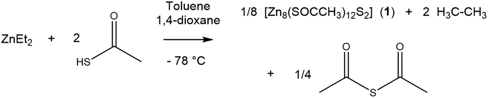 | (1) |
In the literature, the monomeric precursor [Zn(SOCCH3)2TMEDA] (TMEDA = tetramethylethylenediamine) in which TMEDA acts as a stabilising ligand was used to deposit ZnS.27 With a view to improving the Zn:O ratio, the cluster compound 1 was targeted. In the synthesis of 1 the use of 1,4-dioxane rather than TMEDA facilitated cluster formation rather than the isolation of a monomer, since 1,4-dioxane does not coordinate to the zinc centre in the way TMEDA does in Nyman et al.'s report.
[Zn8(SOCCH3)12S2] (1) crystallised out of a concentrated solution of toluene and 1,4-dioxane as centrosymmetric clusters in the monoclinic C2/c space group (Table 1) with eight zinc centres; four of which are unique and four of which are symmetrically generated about an inversion centre (Fig. 1). The cluster consists of two Zn4S6+ cores with thioacetate ligands bridging pairs of Zn2+ centres. This bears close similarity to the structure of basic zinc acetate, which has a central oxygen atom, rather than a sulfur atom (as in 1) coordinated to four zinc centres.28 Zinc acetate is one of the most well known precursors to zinc oxide films, especially via AACVD, and so this structural similarity is promising for the use of 1 as an AACVD precursor to Zn(O,S).29,30 The Zn–O bond distances in 1 (Table 2) are comparable to those in basic zinc acetate, (Zn acetate O–Zn = 1.966 Å, Zn–OCCH3 = 1.976 Å). Zn2–O2 has a shorter bond length (1.9882(16) Å) as compared to Zn2–O1 (1.9972(19) Å) and bond lengths are statistically significantly different. This is expected since the former bond is part of a six membered ring whilst the latter is part of a ten membered ring and therefore experiences lesser bond strain. The same effect is observed for the bond pair Zn2–S1 and Zn2–S2, where the Zn2–S1 bond length is longer than the Zn2–S2 bond length.
| Compound | 1 |
|---|---|
| Empirical formula | C24H36O12S14Zn8 |
| Formula weight/g mol−1 | 1488.33 |
| Crystal system | Monoclinic |
| Space group | C2/c |
| a/Å | 22.8318(2) |
| b/Å | 22.2511(2) |
| c/Å | 12.24570(10) |
| α/° | 90 |
| β/° | 102.3260(10) |
| γ/° | 90 |
| Volume/Å3 | 6077.81(9) |
| Z | 4 |
| ρ calc/g cm−3 | 1.627 |
| Reflections collected | 62293 |
| Independent reflections | 6355 [Rint = 0.0478, Rsigma = 0.0188] |
| Data/restraints/parameters | 6355/0/313 |
| Goodness-of-fit on F2 | 1.022 |
| Final R indexes [I ≥ 2σ (I)] | R 1 = 0.0290, wR2 = 0.0783 |
| Final R indexes [all data] | R 1 = 0.0311, wR2 = 0.0807 |
 | ||
| Fig. 1 Crystal structure of [Zn8(SOCCH3)12S2] (1) with thermal ellipsoids drawn at 50% probability, H atoms omitted for clarity. Grey, purple, red and yellow atoms represent carbon, zinc, oxygen and sulfur respectively. (Symmetry operator: 3/2 − X, 3/2 − Y, 1 − Z.) | ||
| Length/Å | Angles/° | ||
|---|---|---|---|
| Zn2–O1 | 1.9972(19) | Zn1–S1–Zn4 | 94.13(2) |
| Zn2–O2 | 1.9882(16) | Zn2–S1–Zn4 | 90.959(19) |
| Zn2–S1 | 2.3141(5) | Zn3–S1–Zn4 | 93.27(2) |
| Zn2–S2 | 2.3032(6) | ||
| Zn1–S1 | 2.3169(6) | ||
| Zn3–S1 | 2.3354(5) | ||
| Zn4–S1 | 2.2944(5) |
On the basis of τ4, the structural parameter for four coordinate structures (τ4 = 0 for square planar, τ4 = 1 for tetrahedral), the degree of distortion in 1 can be quantified.31 All four zinc centres, and the coordinated sulfur atom S1 adopt pseudo-tetrahedral coordination, with Zn3 having the closest value to 1. The central sulfur atom adopts an almost perfect triangular based pyramid structure, with the Zn1–S1–Zn4, Zn2–S1–Zn4 and Zn3–S1–Zn4 bond angles varying little from 90° (Table 2) whilst Zn1, Zn2, Zn3 and S1 almost lie in the same plane.
During thermolysis of the 1, it is likely that the Zn4S6+ cores remain intact, and the bridging thioacetate ligands break away from the cluster. This is corroborated by thermogravimetric analysis (TGA) data (ESI†), which shows a final mass of 61% at 500 °C corresponding to the mass of the two sets of Zn4S6+ cores within 1. The shortest bonds in the structure are C–O bonds; C–S bonds are also shorter than Zn–O/Zn–S bonds (ESI†) which may explain why the bridging ligands are easily removed to form the anhydride in preference to the decomposition of both the Zn4S6+ centre and thioacetate ligands.
AACVD of Zn(O,S)
Attempts to deposit Zn(O,S) from alternative precursors from the literature (zinc acetate dihydrate and zinc diethyldithiocarbamate) via AACVD all produced films with unsuitable electronic properties (resistance >100 MΩ, see ESI†). As such, compound 1 was designed and synthesised as detailed above to act as the sulfur source in a dual source AACVD reaction towards Zn(O,S). It is postulated that the pseudo-tetrahedral arrangement of the four zinc centres around the sulfur atom in 1 is similar to the tetrahedral arrangement of atoms in bulk wurtzitic ZnS and ZnO, which may make the process of deposition more energetically favourable. The oxygen source for the deposition of Zn(O,S) was chosen to be MeOH as it is well known that the AACVD reaction of ZnEt2 with MeOH produces highly conductive ZnO films.32The suitability of 1 for AACVD was investigated under a range of conditions, including the deposition of the binary material ZnS (ESI†). It was found that films of Zn(O,S) with optoelectronic properties comparable with buffer layer materials were grown by the dual source AACVD reaction of 1 with ZnEt2 and MeOH at 500 °C. The film was transparent, showed good coverage across the glass substrate and was well adhered; passing the Scotch™ tape test and was not scratched by a steel stylus.
 | ||
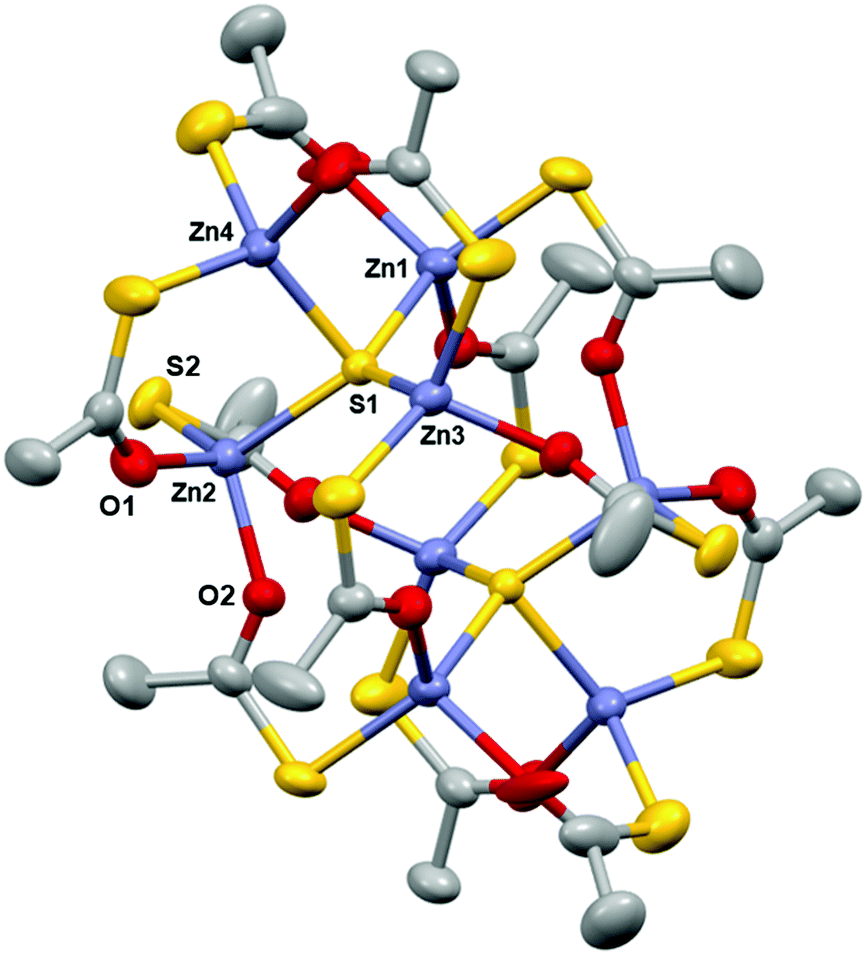
| Fig. 2 X-ray diffraction pattern of ZnO0.884S0.116 showing peak shifting to lower 2θ values relative to ZnO. | ||
Peak shifting to lower 2θ values relative to the peaks of pure ZnO indicated substitution of O atoms with S atoms which is consistent with the expansion of the unit cell due to the increased atomic radius of S (0.88 Å) as compared to O (0.48 Å).34
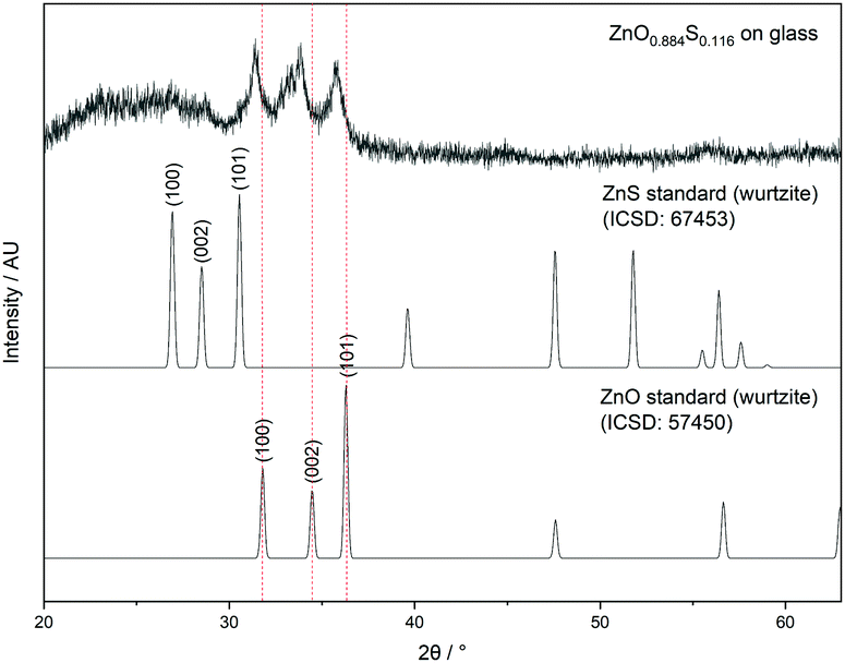
X-ray photoelectron spectroscopy (XPS) analysis confirmed the presence of oxygen (see ESI†), zinc and sulfur in the film. Only one environment for zinc was present in the XPS which further corroborates the formation of Zn(O,S) and not a mixture of the binary oxide or sulfide materials (Fig. 3, top).
 | ||
| Fig. 3 XPS of the Zn 2p1/2 and 2p3/2 states peaks at 1044.7 eV and 1021.6 eV binding energy respectively, top; and the S 2p1/2 and 2p3/2 peaks at 162.4 eV and 161.4 eV respectively, bottom, both at a 300 s etch. | ||
The states appeared at binding energies of 1044.7 eV and 1021.6 eV (Zn 2p1/2 and 2p3/2 respectively) which is consistent with the formation of Zn(O,S) when compared to the literature value of 1021.74 eV (Zn 2p3/2) for a Zn(O,S) film with S/Zn ratio = 0.1 as reported by Platzer-Björkman et al.4 It should be noted however, that the binding energy for Zn in ZnO and ZnS are similar (2p3/2 = 1022.1 eV and 1022.0 eV respectively).35 There was one S environment present, whose 2p1/2 and 2p3/2 states appeared at binding energies of 162.4 eV and 161.4 eV respectively (Fig. 3, bottom). This is comparable to the 2p3/2 state in ZnS which appears at 161.6 eV, with the downshift in energy values for the S states in the Zn(O,S) film further indicating formation of the oxysulfide as opposed to binary oxides or sulfides.36 Additionally, XPS was used to estimate the elemental ratio of Zn and S in the film and this was found to be 0.078 which would give a chemical formula of ZnO0.922S0.078 for the film.
Scanning electron microscopy (SEM) images revealed films were made up of a fully connected array of particles consistent with the observed low resistivity. The size of particulates varies across the surface and this is likely due to the use of two different solvents in the dual source AACVD process. Cross-sectional SEM showed the film to have a thickness of ∼2.5 μm.
Interestingly, the energy dispersive X-ray (EDX) analysis of the film gives a general formula of ZnO0.884S0.116, a higher sulfur content than the formula derived from XPS analysis. The discrepancies between the elemental composition for the two techniques can be accredited to the fact that EDX covers thicknesses of about 2–3 μm and therefore any compositional variation through the thickness of the film is not accounted for (Fig. 4), and instead an average of the elemental ratios is obtained. XPS scans at a 300 s etch average lower values which suggests that perhaps a higher S/Zn ratio is seen closer to the substrate. Therefore, EDX will give a value for composition for the chemical formula throughout the depth of the film and this difference between EDX and XPS is evidence for compositional variation through the thickness of the film from surface to substrate. This film is ∼2.5 μm thick, and the increase in calculated sulfur content from XPS to EDX is 3.8%, however as films get thinner the compositional variation decreases. This observation is crucial for potential application of these materials, since buffer layers ideally need to be considerably thinner (∼30 nm).
 | ||
| Fig. 4 SEM of Zn(O,S) film: cross section SEM image at × 3700 showing film thickness of 2.5 μm, inset: plane view at ×17000. Selected areas show penetration depths of XPS (red) and EDX (blue) techniques. | ||
| N/cm−3 | μ/cm2 V−1 s−1 | ρ/Ω cm | |
|---|---|---|---|
| ZnO0.884S0.116 | 1.36 × 10¹⁹ | 15.34 | 0.02998 |
| ZnO0.75S0.25 | 1.7 × 10¹⁸ | 36.1 | 0.101 |
| ZnO | 1.75 × 10²⁰ | 16.96 | 0.00210 |
Mapping of a large area film
The commercial application of Zn(O,S) will require large area deposition and so the investigation of compositional variation is necessary. Large area films (5 × 4 cm) were deposited, and mapping was used to probe the variation from the AACVD reactor inlet to exhaust, facilitating correlation of composition and structure with optoelectronic properties.Large area films of Zn(O,S) were deposited by the dual source AACVD reaction of 1 with ZnEt2 and MeOH at 500 °C. As in the previous section, films adhered to the glass substrate and showed excellent coverage. For the analysis, all positions were characterised by a range of techniques and Fig. 5 shows the grid reference system used.
 | ||
| Fig. 5 Zn(O,S) film with the superimposed grid reference system used throughout, left. XRD patterns of all positions, right. | ||
The XRD patterns at all positions on the film showed the characteristic broadness and amorphous nature of Zn(O,S) films from the literature (Fig. 5, right). Patterns are shown from 25–40 2θ for ease of comparison (full data in ESI†). Again, 2θ values are lower relative to the peaks of pure ZnO owing to the aforementioned substitution of O with S. All positions had similar absolute peak shifts of the three principle peaks of ZnO (∼0.4° for (100) and ∼0.6° for (002) and (101)). It is interesting to observe that some patterns have very few features, for example A1, B1 and C1, this can be linked to composition and properties (Fig. 6 left, blue area, Table 4). The structural variation across the film may be attributed to the non-uniform temperature of the CVD rig, with variations of up to 15 °C from the centre of the rig to the edges.
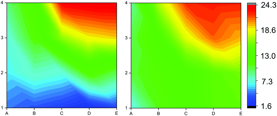 | ||
| Fig. 6 Contour maps showing the S/Zn ratio across the film calculated from XPS (left) and EDX (right). | ||
| Resistance/MΩ | N/cm−3 | μ/cm2 V−1 s−1 | ρ/Ω cm | (100) peak position/2θ | Formula from XPS | Formula from EDX | T λ550/% | |
|---|---|---|---|---|---|---|---|---|
| A1 | 3.5 | — | — | — | 31.50 | ZnO0.954S0.046 | ZnO0.931S0.069 | 100 |
| A2 | 0.7 | 1.49 × 10¹⁹ | 14.03 | 0.02992 | 31.48 | ZnO0.937S0.063 | ZnO0.897S0.103 | 92.7 |
| A3 | 0.6 | 1.66 × 10¹⁹ | 13.73 | 0.02732 | 31.23 | ZnO0.928S0.072 | ZnO0.900S0.100 | 86.9 |
| A4 | 1 | 1.36 × 10¹⁹ | 10.42 | 0.04414 | 31.30 | ZnO0.909S0.091 | ZnO0.913S0.087 | 75.0 |
| B1 | 1.2 | — | — | — | 31.48 | ZnO0.963S0.037 | ZnO0.892S0.108 | 100 |
| B2 | 0.6 | 1.36 × 10¹⁹ | 15.34 | 0.02998 | 31.36 | ZnO0.922S0.078 | ZnO0.884S0.116 | 91.2 |
| B3 | 1.5 | 9.60 × 10¹⁸ | 11.22 | 0.05794 | 31.35 | ZnO0.887S0.113 | ZnO0.870S0.130 | 83.2 |
| B4 | 5.1 | — | — | — | 31.15 | ZnO0.874S0.126 | ZnO0.829S0.171 | 71.3 |
| C1 | 1.1 | — | — | — | 31.41 | ZnO0.971S0.029 | ZnO0.874S0.126 | 100 |
| C2 | 0.7 | 1.62 × 10¹⁹ | 11.77 | 0.0327 | 31.22 | ZnO0.929S0.071 | ZnO0.870S0.130 | 100 |
| C3 | 3.3 | 9.12 × 10¹⁸ | 4.523 | 0.1512 | 31.19 | ZnO0.836S0.164 | ZnO0.819S0.181 | 74.0 |
| C4 | 33.4 | — | — | — | 31.11 | ZnO0.764S0.236 | ZnO0.777S0.223 | 69.1 |
| D1 | 5.1 | — | — | — | 31.23 | ZnO0.984S0.016 | ZnO0.855S0.145 | 80.6 |
| D2 | 1 | 2.15 × 10¹⁹ | 6.73 | 0.04317 | 31.08 | ZnO0.881S0.119 | ZnO0.854S0.146 | 74.5 |
| D3 | 5.8 | — | — | — | 31.17 | ZnO0.812S0.188 | ZnO0.786S0.214 | 74.9 |
| D4 | 46.7 | — | — | — | 31.19 | ZnO0.759S0.241 | ZnO0.773S0.227 | 67.2 |
| E1 | 2.4 | — | — | — | 31.34 | ZnO0.968S0.032 | ZnO0.853S0.147 | 80.9 |
| E2 | 1.5 | 1.36 × 10¹⁹ | 7.742 | 0.05924 | 31.22 | ZnO0.900S0.100 | ZnO0.845S0.155 | 81.7 |
| E3 | 12.4 | — | — | — | 31.26 | ZnO0.805S0.195 | ZnO0.801S0.199 | 70.0 |
| E4 | 81.7 | — | — | — | 31.19 | ZnO0.757S0.243 | ZnO0.775S0.225 | 69.2 |
To probe the composition of the film across the grid, both XPS and EDX were used to calculate S/Zn ratios. XPS and EDX were performed on all positions shown in Fig. 5 and these data were linearly interpolated to show the S/Zn ratios as contour maps (Fig. 6).
Both XPS and EDX analysis showed similar trends from the reactor inlet to exhaust, with the S/Zn ratio increasing from the reactor inlet to the exhaust, as indicated in Fig. 6. The blue areas closest to the inlet indicate lower levels of sulfur doping, the green areas indicate 10–12% sulfur doping and the red areas indicate higher levels of sulfur doping in the Zn(O,S) films. As film thickness can be optimised, thinner films will have a smaller degree of compositional variation which will be promising for the incorporation of this material into thin film solar cells.
Hall effect measurements were carried out on the film to determine electronic properties at each position on the grid and compare this to the variation in the composition. Omissions at certain positions in Table 4 indicate that these points were either too resistive or did not make good contact with the Hall measurement system probe. Clearly there is a change in composition from inlet to exhaust in the large area film, as shown by both XPS and EDX. This variation in composition has a large effect on the optical properties as summarised in Table 4 below. UV/vis spectroscopy was used to estimate the optical band gaps across the film using Tauc plots (UV/vis spectra of all positions in ESI†). As the role of a buffer layer is to improve the interface between the absorber and the transparent conducting oxide (TCO), the buffer layer should have a band gap between that of the absorber (1.0–1.5 eV) and the TCO (>3 eV), so as to reduce the conduction band offset (CBO). It must be noted that band gap estimations using the Tauc relation have a large margin of error associated with them and so definitive values taken through this approach may not be representative of the actual material in question. The band gap energies obtained increase from reactor inlet to exhaust, corresponding with increasing sulfur content (Fig. 7). The range of energies lies between 3.74 eV and 3.93 eV and this observation is in agreement with the increase in the optical band gap of pure ZnS as compared to pure ZnO.
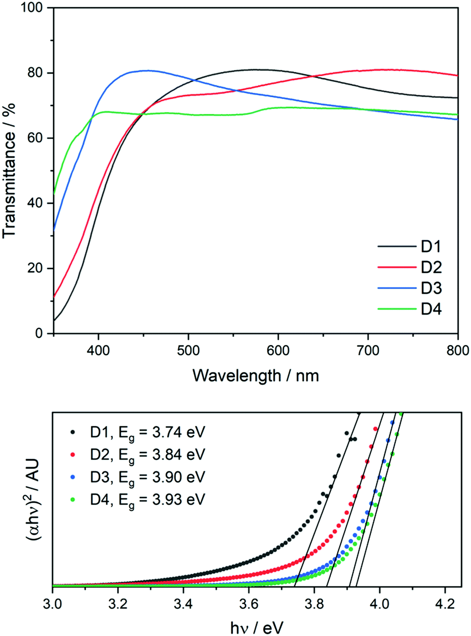 | ||
| Fig. 7 UV/vis transmittance spectra of positions D1–D4 (top) and Tauc plots of positions D1–D4 showing their optical band gaps (bottom). | ||
Whilst the band gap energies lie in the correct range, other factors that must be considered are the energies of the conduction band and valence band edges. These must also be compatible with the band edges of the absorber and TCO. The physical variable that represents these energies is the work function. Literature values suggest that the range of values for the work function of Zn(O,S) is 2.95 eV (ZnS)–3.91 eV (ZnO).11 Though the calculation of these values is beyond the scope of this work, it must be considered when constructing a PV cell architecture.
From the data in Table 4, it is clear that Hall effect data cannot be obtained for parts of the film where the resistance is greater than 3.3 MΩ. Comparing this to the S/Zn ratios from XPS and EDX contour plots, this is consistent with higher sulfur doping, as expected. Point B2 shows the highest electron mobility, as well as a high charge carrier concentration, a low resistivity, and high transparency, consistent with the film reported in the previous section with the formula ZnO0.884S0.116 derived from EDX analysis.
Electronic properties with potential for application in buffer layer materials lie between the values of 9.12 × 10¹⁸–1.66 × 1019 cm−3 for charge carrier concentration, which correspond to S/Zn ratios of 0.11–0.15 which corresponds with the green bands in Fig. 6. Whilst the cause of these large area variations in composition and properties may be due to a range of variables (reactor temperature, flow turbulence, decomposition profile of precursors), they are undoubtedly present in much of the AACVD literature. The method presented here, utilising combinatorial analytical techniques with single film deposition, is a good way to assess variations in films produced via AACVD from reactor inlet to exhaust and improve material properties in future depositions.37,38
Conclusions
We have shown the deposition of conductive films of Zn(O,S) from the dual source AACVD reaction of ZnEt2, MeOH and the precursor [Zn8(SOCCH3)12S2] (1). This is the first instance of Zn(O,S) thin films being deposited via solution based CVD. The film ZnO0.884S0.116 exhibited excellent transparency (>90%), high conductivity and a high charge carrier concentration, consistent with values from the literature, making it an appropriate buffer layer material. It was also found that the film varies through its depth as corroborated by XPS and EDX analysis, with sulfur segregation in areas closer to the substrate.Following the deposition of large area films, the compositional, structural and optoelectronic variation across films was analysed in a combinatorial fashion and it was found that the S/Zn ratio increased from reactor inlet to exhaust. The range of band gap energies increased from inlet to outlet (3.74 eV and 3.93 eV), which was consistent with other results presented in this work. These results were shown to be linked to optical transparency and electronic properties, with an optimum sulfur doping of 11–15% giving the most suitable buffer layer material.
Conflicts of interest
There are no conflicts to declare.Acknowledgements
The authors would like to thank the EPSRC (EP/R513143/1) and Pilkington NSG for supplying the glass substrates. Mr Stephen Boyer (London Metropolitan University) is thanked for carrying out elemental analysis. Mr Samuel Douglas is thanked for carrying out TGA.Notes and references
- P. D. Matthews, P. D. McNaughter, D. J. Lewis and P. O’Brien, Chem. Sci., 2017, 8, 4177–4187 RSC.
- S. R. Thomas, P. Pattanasattayavong and T. D. Anthopoulos, Chem. Soc. Rev., 2013, 42, 6910 RSC.
- A. D. Martinez, A. N. Fioretti, E. S. Toberer and A. C. Tamboli, J. Mater. Chem. A, 2017, 5, 11418–11435 RSC.
- C. Platzer-Björkman, T. Törndahl, D. Abou-Ras, J. Malmström, J. Kessler and L. Stolt, J. Appl. Phys., 2006, 100, 044506 CrossRef.
- P. Sinsermsuksakul, K. Hartman, S. Bok Kim, J. Heo, L. Sun, H. Hejin Park, R. Chakraborty, T. Buonassisi and R. G. Gordon, Appl. Phys. Lett., 2013, 102, 053901 CrossRef.
- T. Ericson, J. J. Scragg, A. Hultqvist, J. T. Watjen, P. Szaniawski, T. Torndahl and C. Platzer-Bjorkman, IEEE J. Photovolt., 2014, 4, 465–469 Search PubMed.
- N. Naghavi, D. Abou-Ras, N. Allsop, N. Barreau, S. Bücheler, A. Ennaoui, C.-H. Fischer, C. Guillen, D. Hariskos, J. Herrero, R. Klenk, K. Kushiya, D. Lincot, R. Menner, T. Nakada, C. Platzer-Björkman, S. Spiering, A. N. Tiwari and T. Törndahl, Prog. Photovolt: Res. Appl., 2010, 18, 411–433 CrossRef.
- B. W. Sanders and A. Kitai, Chem. Mater., 1992, 4, 1005–1011 CrossRef CAS.
- J. R. Bakke, J. T. Tanskanen, C. Hägglund, T. A. Pakkanen and S. F. Bent, J. Vac. Sci. Technol. A, 2012, 30, 01A135 CrossRef.
- S. K. Pandey, S. Pandey, V. Parashar, R. S. Yadav, G. K. Mehrotra and A. C. Pandey, Nanoscale, 2014, 6, 1602–1606 RSC.
- L. A. Burton and A. Walsh, Appl. Phys. Lett., 2013, 102, 132111 CrossRef.
- B. K. Meyer, A. Polity, B. Farangis, Y. He, D. Hasselkamp, Th. Krämer and C. Wang, Appl. Phys. Lett., 2004, 85, 4929–4931 CrossRef CAS.
- C. Persson, C. Platzer-Björkman, J. Malmström, T. Törndahl and M. Edoff, Phys. Rev. Lett., 2006, 97, 146403 CrossRef PubMed.
- T. M. Friedlmeier, P. Jackson, A. Bauer, D. Hariskos, O. Kiowski, R. Wuerz and M. Powalla, IEEE J. Photovolt., 2015, 5, 1487–1491 Search PubMed.
- P. Sinsermsuksakul, L. Sun, S. W. Lee, H. H. Park, S. B. Kim, C. Yang and R. G. Gordon, Adv. Energy Mater., 2014, 4, 1400496 CrossRef.
- H. Hejin Park, R. Heasley and R. G. Gordon, Appl. Phys. Lett., 2013, 102, 132110 CrossRef.
- S. Sinha, H. V. Ramasamy, D. K. Nandi, P. N. Didwal, J. Y. Cho, C.-J. Park, Y.-S. Lee, S.-H. Kim and J. Heo, J. Mater. Chem. A, 2018, 6, 16515–16528 RSC.
- C. E. Knapp and C. J. Carmalt, Chem. Soc. Rev., 2016, 45, 1036–1064 RSC.
- S. Sathasivam, R. R. Arnepalli, B. Kumar, K. K. Singh, R. J. Visser, C. S. Blackman and C. J. Carmalt, Chem. Mater., 2014, 26, 4419–4424 CrossRef CAS.
- D. S. Bhachu, D. O. Scanlon, E. J. Saban, H. Bronstein, I. P. Parkin, C. J. Carmalt and R. G. Palgrave, J. Mater. Chem. A, 2015, 3, 9071–9073 RSC.
- K. Ramasamy, M. A. Malik and P. O’Brien, Chem. Sci., 2011, 2, 1170 RSC.
- M. A. Malik, M. Afzaal and P. O’Brien, Chem. Rev., 2010, 110, 4417–4446 CrossRef CAS PubMed.
- P. Marchand, I. A. Hassan, I. P. Parkin and C. J. Carmalt, Dalton Trans., 2013, 42, 9406 RSC.
- P. Kevin, M. A. Malik and P. O’Brien, New J. Chem., 2015, 39, 7046–7053 RSC.
- A. C. Jones and M. L. Hitchman, Chemical Vapour Deposition: Precursors, Processes and Applications, Royal Society of Chemistry, Cambridge, UK, 2009 Search PubMed.
- D. S. Bhachu, S. J. A. Moniz, S. Sathasivam, D. O. Scanlon, A. Walsh, S. M. Bawaked, M. Mokhtar, A. Y. Obaid, I. P. Parkin, J. Tang and C. J. Carmalt, Chem. Sci., 2016, 7, 4832–4841 RSC.
- M. Nyman, M. J. Hampden-Smith and E. N. Duesler, Chem. Vap. Deposition, 1996, 2, 171–174 CrossRef CAS.
- H. Koyama and Y. Saito, Bull. Chem. Soc. Jpn., 1954, 27, 112–114 CrossRef CAS.
- M. R. Waugh, G. Hyett and I. P. Parkin, Chem. Vap. Deposition, 2008, 14, 366–372 CrossRef CAS.
- S. Chen, R. M. Wilson and R. Binions, J. Mater. Chem. A, 2015, 3, 5794–5797 RSC.
- L. Yang, D. R. Powell and R. P. Houser, Dalton Trans., 2007, 955–964 RSC.
- S. D. Ponja, S. Sathasivam, I. P. Parkin and C. J. Carmalt, RSC Adv., 2014, 4, 49723–49728 RSC.
- S. Y. Yu, M. A. Hassan, M. A. Johar and S.-W. Ryu, J. Korean Phys. Soc., 2018, 73, 649–655 CrossRef CAS.
- E. Clementi, D. L. Raimondi and W. P. Reinhardt, J. Chem. Phys., 1967, 47, 1300–1307 CrossRef CAS.
- G. Deroubaix and P. Marcus, Surf. Interface Anal., 1992, 18, 39–46 CrossRef CAS.
- K. Laajalehto, I. Kartio and P. Nowak, Appl. Surf. Sci., 1994, 81, 11–15 CrossRef CAS.
- A. Kafizas and I. P. Parkin, J. Am. Chem. Soc., 2011, 133, 20458–20467 CrossRef CAS PubMed.
- A. Kafizas and I. P. Parkin, Chem. Soc. Rev., 2012, 41, 738–781 RSC.
Footnote |
| † Electronic supplementary information (ESI) available. CCDC 1972529. For ESI and crystallographic data in CIF or other electronic format see DOI: 10.1039/d0tc00840k |
| This journal is © The Royal Society of Chemistry 2020 |