
 Open Access Article
 This Open Access Article is licensed under a
 Creative Commons Attribution 3.0 Unported Licence
Plasma CVD of B–C–N thin films using triethylboron in argon–nitrogen plasma
Laurent
Souqui
 ,
Justinas
Palisaitis
,
Hans
Högberg
and
Henrik
Pedersen
*
,
Justinas
Palisaitis
,
Hans
Högberg
and
Henrik
Pedersen
*
Department of Physics, Chemistry and Biology, Linköping University, SE-581 83 Linköping, Sweden. E-mail: henrik.pedersen@liu.se
First published on 18th February 2020
Abstract
Amorphous boron–carbon–nitrogen (B–C–N) films with low density are potentially interesting as alternative low-dielectric-constant (low-κ) materials for future electronic devices. Such applications require deposition at temperatures below 300 °C, making plasma chemical vapor deposition (plasma CVD) a preferred deposition method. Plasma CVD of B–C–N films is today typically done with separate precursors for B, C and N or with precursors containing B–N bonds and an additional carbon precursor. We present an approach to plasma CVD of B–C–N films based on triethylboron (B(C2H5)3), a precursor with B–C bonds, in an argon–nitrogen plasma. From quantitative analysis with time-of-flight elastic recoil detection analysis (ToF-ERDA), we find that the deposition process can afford B–C–N films with a B/N ratio between 0.9–1.3 and B/C ratios between 3.4–8.6 and where the films contain from 3.6 to 7.8 at% H and from 6.6 to 20 at% O. The films have low density, from 0.32 to 1.6 g cm−3 as determined from cross-section scanning electron micrographs and ToF-ERDA with morphologies ranging from smooth films to separated nanowalls. Scanning transmission electron microscopy shows that C and BN do not phase-separate in the film. The static dielectric constant κ, measured by capacitance–voltage measurements, varies with the Ar concentration in the range from 3.3 to 35 for low and high Ar concentrations, respectively. We suggest that this dependence is caused by the energetic bombardment of plasma species during film deposition.
Introduction
The continued miniaturization of electronic devices requires a range of advances within materials technology. One such an example is the development of materials with low dielectric constant (low-κ) and high structural integrity to allow for thinner layers with better electrical insulation between interconnects in back end of line (BEOL) processing.1 From intrinsic high mechanical properties and an ability to form stable amorphous network solids, hydrogenated amorphous boron carbides (BxC:H) are considered as promising next generation low-κ materials.2 As boron nitride (BN) and boron carbonitrides (B–C–N) exhibit properties similar to that shown by BxC:H, this further increases the family of possible low-κ materials to include BN and B–C–N suggesting studies of the properties of these materials.Deposition of low-κ materials require process temperatures below 300 °C to avoid diffusion of underlaying metallic interconnect layers.1 A chemical vapor deposition (CVD) process where a plasma discharge is used to activate the deposition chemistry at low thermal energy3 is therefore favorable for BEOL processing. Several studies on plasma CVD of B–C–N films in the literature have been conducted with precursors containing B–N bonds such as: dimethylamineboron (DMAB, (H3C)HN:BH3)4 pyridine-borane (PB, C5H5NBH3),5 triazaborabicyclodecane (TBBD, BN(NHC3H2)2),5 1,3,5-trimethylborazine (N-TMBA, (CH3)3N3B3H3),6–9 1,3,5-triethylborazine (N-TEBA, B3H3(NCH2CH3)3),10,11 tris-(dimethylamino)boron (TDMAB, B(N(CH3)2)3),12 triethylamineboron7 and trimethylamineboron.13,14 The incorporation of nitrogen in the films has been found to be important to increase the bandgap in B–C–N materials, making them more insulating.15 The highest nitrogen content achieved without additional nitrogen source in the plasma CVD process are 28 at% using N-TMBA,6 43 at% using N-TEBA,10 38 at% using TDMAB,12 20 at% using triethylamineboron7 and, 12 at% using trimethylamineboron.13 Studies on the deposition chemistry suggest that the B–N bonds in the precursor molecules are not the major source of nitrogen in the film,13,14 and ammonia (NH3) or dinitrogen (N2) are typically added to the plasma to increase the N content in the films. As volatile boron compounds with B–C (such as akylborons) are more readily available than volatile boron compounds with B–N bonds, they might therefore be an appealing alternative route for plasma CVD of B–C–N films.
Here, we investigate plasma CVD of B–C–N films using triethylboron (TEB, B(C2H5)3) as precursor for B and C with N2 as nitrogen precursor. TEB has previously been studied as precursor for plasma CVD of BxC films,16 and have been shown to result in deposition of films with B/C ratios of 1.0–1.7, increasing with higher applied plasma power. TEB was further suggested to decompose by a β-elimination mechanism in the plasma to form BH3 and C2H4 which decompose further to the optically detected BH, CH, C2 and H species. To determine how addition of N2 to the plasma affects the deposition chemistry, we studied the effect of plasma power, total gas flow and N/Ar ratio on the film deposition and the film properties, using a factorial plan-like approach. Two deposition regimes could be determined depending on whether the films are deposited in a N-rich plasma or an Ar-rich plasma. The deposited films were found to exhibit a high B and N content with a B/N ratio close to 1, almost regardless of the deposition conditions, while the C content was found to vary somewhat without clear dependence to the deposition parameters. The high boron content and the nanostructure of the films are of potential interested for organic-based neutron detectors, as for BN17 and BxC.18 Low κ-values of around 3 were measured for films deposited at low Ar partial pressure.
Experimental details
Film deposition
The depositions of the B–C–N films were performed in a microwave plasma CVD reactor (ASTEX 2.45 GHz) held at a base pressure below 3 Pa. The inner diameter of the chamber was 14 cm and the diameter of the graphite sample holder, which was neither heated, biased, nor grounded, was 12 cm. The deposition temperature was between 300–400 °C as previously estimated for this PACVD system. A more detailed description of the plasma CVD system can be found in ref. 19. During deposition, the valve to the dry rotary vane pump of the reactor was fully opened, meaning that the pressure in the system was controlled by the applied gas flow. For all experiments, the plasma power, maximum 2500 W, was defined as the set value of power delivered to the microwave generator with the readout value of the reflected power subtracted. The reflected power was minimized by adjusting three tuning stubs on the wave guide.Full 100 mm-Si(100) wafers were used as substrates. The substrates were cleaned in an ultrasonic bath by dipping 5 minutes in acetone followed by 5 minutes in ethanol. Prior to deposition a 1500 W argon plasma was ignited for 15 minutes to outgas the chamber using 99.9997% purity Ar. The plasma was then turned off and N2 (99.999% purity) and TEB, SAFC Hitech, semiconductor grade purity, kept in a stainless-steel bubbler maintained at 5 °C by a thermostat bath and with Ar used as bubbling gas were inserted in the reaction cell. After 2 min, once the gas flows were stabilized, a 1450 W Ar–N2–TEB plasma was ignited and the power adjusted to the desired growth conditions. Films where deposited for deposition times varying between 3.2 and 75 minutes. To study the deposition process, we adopted a factorial plan-like approach20 with the TEB flow (FTEB), the total gas flow (FTotal), the N/Ar ratio  and the plasma power (PPlasma) as parameters. The parameters were assigned three levels, the values corresponding to each level are summarized in Table 1. The (N2 + Ar)/TEB ratio was fixed to 30 throughout the study, meaning that FTEB and FTotal are interconnected parameters in the study. The values for the gas flows and the maximum power were limited by the plasma CVD reactor. From previous experience on plasma CVD of BxC:H films, a minimum plasma power of 1500 W was set.16 The logarithm of
  was used for linearity.
| Level | TEB flow (sccm) | Total flow (sccm) | log(N/Ar) | Plasma power (W) |
|---|---|---|---|---|
| Minimum (−1) | 2.6 | 80 | −1.12 | 1450 ± 50 |
| Centre (0) | 5.1 | 158 | 0 | 1888 ± 62 |
| Maximum (+1) | 7.7 | 238 | 1.12 | 2325 ± 75 |
The dependence of a quantity A on the three independent parameters could be described as:
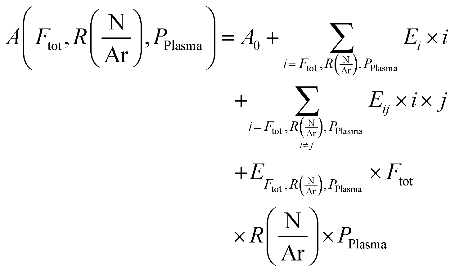
 are respectively the effects of each parameters, the effect of the interaction between two parameters and the effect of the three parameters. The significance of a parameter was evaluated by analysis of variance (so-called 3-way ANOVA).21 As the factorial plan assumes the linearity of the model, we performed depositions in the center of the experimental space and compared them with the predictions given by the model to test its accuracy. The experiments performed in the present work are summarized in Table 2.
| Total flow (sccm) | Plasma power (W) | log(N/Ar) |
|
|---|---|---|---|
| 80 | 1450 ± 50 | −1.12 | [−1, −1, −1] |
| 80 | 1450 ± 50 | 1.12 | [−1, −1, 1] |
| 80 | 2325 ± 75 | −1.12 | [−1, 1, −1] |
| 80 | 2325 ± 75 | 1.12 | [−1, 1, 1] |
| 238 | 1450 ± 50 | −1.12 | [1, −1, −1] |
| 238 | 1450 ± 50 | 1.12 | [1, −1, 1] |
| 238 | 2325 ± 75 | −1.12 | [1, 1, −1] |
| 238 | 2325 ± 75 | 1.12 | [1, 1, 1] |
| 158 | 1888 | 0 | [0, 0, 0] |
| 158 | 1888 | 1.12 | [0, 1, 0] |
Characterization
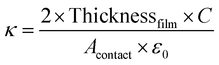
The plasma composition was studied by optical emission spectroscopy (OES), using a Mechelle Sensicam 900 spectrometer (Multichannel Instruments) with a spectral resolution of λ/Δλ > 900. Emission spectra of the plasma during the film deposition process were recorded in a wavelength range from 320 to 1050 nm. Fourier transform infrared spectroscopy (FTIR) reflectance spectra were measured in a Bruker VERTEX 70 equipment using p-polarized light at an incident angle of 51.2° with respect to the sample surface normal. The spectra were acquired at room temperature, after a 30 min N2 purge, with 2 cm−1 resolution and averaged over 50 scans. A gold thin film was used as reference. Time-of-flight elastic recoil detection analysis (ToF-ERDA) was used to determine the composition and the density of the films. The measurements were performed at the Tandem Laboratory at Uppsala University using a 36 MeV 127I7+ beam. The incident angle of primary ions and exit angle of recoils were both set at 67.5° with respect to the sample surface normal, giving a recoil angle of 45°. The measured ToF-ERDA spectra were converted into relative atomic concentration profiles using the Potku code.22 X-ray photoelectron spectroscopy (XPS) was used to study the chemical bonding structure of the films. The XPS instrument (AXIS Ultra DLD from Kratos Analytical) used monochromatic Al Kα radiation (hν = 1486.6 eV), operated at a base pressure of 1.5 × 10⁻⁷ Pa and with the X-ray anode set to 225 W during analysis. The binding energy scale was calibrated by setting the position of the Fermi edge of a sputter cleaned Ag sample to 0.0 eV23 resulting in the position of the Ag 3d5/2 core level peak of 368.30 eV.24 The samples were sputter cleaned for 180 s with 0.3 keV Ar ions incident at an angle of 70° with respect to the surface normal to remove the adventitious contamination due to exposure to air. The Casa XPS software (version 2.3.16) was used for quantitative analysis with elemental sensitivity factors supplied by Kratos Analytical Ltd.25 The thickness and the morphology of the film were studied by scanning electron microscopy (SEM, Gemini) using an in-lens detector and an accelerating voltage of 5 kV. The sample for the scanning transmission electron microscopy (STEM) analysis was prepared by removing the film from the substrate using a blade and dispersing it onto the lacey carbon suspended by the copper grid. STEM characterization was performed using the Linköping double Cs corrected FEI Titan3 60–300 operated at 300 kV. STEM high angle annular dark field (STEM-HAADF) images were acquired using strong mass-contrast (Z-contrast) conditions. The elemental constituents of the film were analysed by core-loss electron energy loss spectroscopy (EELS) mapping. Core-loss EELS spectrum images of 40 px × 40 px were recorded using 0.25 eV per channel energy dispersion and 0.3 s dwell time for each pixel which were used to extract the B, C, N and O distribution maps. The crystal structure of the films was assessed by Grazing incidence X-ray diffraction (GI-XRD), using a diffractometer (PANAlytical Empyrean) with a Cu Kα X-ray source and an open detector (PIXcel3D). The diffractometer was equipped with an X-ray mirror and 1/16° divergence slit on the primary side and a parallel plate collimator on the secondary side. The low-frequency dielectric constant of the films was determined from 100 kHz capacitance–voltage (CV) measurements using scanning voltage from −10 V to 10 V and 200 nm evaporated Al contacts on the deposited films. Measurements where conducted using two adjacent contacts of the same size. Three contact sizes, diameter of 0.5, 0.8 and 1.2 mm, were used and compared. The dielectric constant was calculated from the CV curve in the accumulation region through the geometric capacitance relationshipWhere C is the measured capacitance, ε0 is the permittivity of free space and A is the area of the Al contacts.
Results and discussion
Plasma characterization
To study the deposition chemistry, we compared the Ar–N2–TEB plasma applied for thin film growth of B–C–N to an Ar–N2 plasma. The OES spectra of the Ar–N2 plasma, represented by black curves in Fig. 1, were dominated by the emission of atomic Ar (persistent lines at 695 nm, 750 nm, 763 nm, 795 nm, 801 nm, 812 nm) and N2 (first and second positive systems),26 traces of H (Balmer lines: Hα, 656 nm; Hβ, 485 nm; Hγ 433 nm), H2 (Fulcher bands at 602, 604 and 605 nm), NH (around 336 nm), CN (violet system, Δν = −1, 0, 1), N2+ (first negative system),26 CH (A2Δ →A2Π at 431.15 nm) and C2 (Swan system, Δν = 0)27 could also be detected. A band at 915 nm was ascribed to CN (Red system28) and sharp low intensity peaks where attributed to N (411 nm), N+ (362 nm) and Ar+ (474, 561 and 685 nm). The presence of species with hydrogen and carbon is believed to be caused by etching of previously deposited coatings on the CVD chamber walls. As TEB was added to the Ar–N2 plasma, the signal from the first positive system of N2 was strongly reduced while signals from H, NH, CH, CN, and C2, are found to increase, as shown by the red curves in Fig. 1 and the bands from C2 (Swan system, Δν = −1 and 1)27 appear. This suggests that the plasma chemistry decomposing the TEB molecule consumes N2 while forming CN as optically active species. The presence of H, CH and C2 and the absence of small, optically active molecules with a B–C bond, such as BC, BC−, BC2 and BC2−,29,30 in the plasma can be explained by the proposed decomposition mechanism for TEB in an Ar plasma where the ethyl ligands are removed by β-elimination forming BH3 and C2H4 with subsequent homolytic cleavage or hydrogen abstraction to form CH and C2, respectively.16 The Ar–N2 plasma in this study seems to follow a similar mechanism with additional formation of CN. In OES, BH interferes with Hγ31 and atomic B could not be detected as B emits essentially in the infrared (1160 nm) or in the UV (250 nm and below) which is outside the range of our spectrometer. This makes the plasma characterization of the B-containing species incomplete. For comparison, OES of plasmas in plasma CVD of GaN and Al2O3 using trimethylgallium and trimethylaluminum, respectively, show that the group 13-element is not present as ions but as neutrals (atomic Ga for GaN,32,33 Al and AlO for Al2O334). This suggests that atomic B participate as a film depositing species in our plasma CVD process. As the TEB molecule contains 15 H atoms per B atom, and the (N2 + Ar)/TEB ratio was fixed to 30, a substantial amount of H is added to the plasma when the TEB is introduced. It could therefore be regarded to change the initial Ar–N2 plasma into an H–Ar–N2 plasma. Consequently, as the signal from the first positive system of N2 decreases, the signal from NH is found to increase when TEB is added to the plasma (see red curve in Fig. 1). This effect is less notable when a high total flow and a high N/Ar in combination with a low plasma power are applied.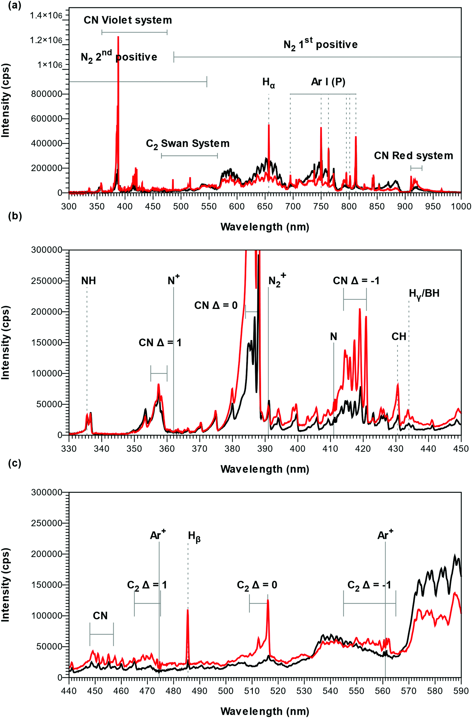 | ||
Fig. 1 Optical emission spectra of the TEB–Ar–N2 plasma during deposition (in red) compared to the pure Ar–N2 (black). The deposition conditions were 2325 W plasma power, 238 sccm total flow and log(N/Ar) = 1.12 i.e. . In the full range spectrum (a), only the visible so-called persistent lines of Ar are indicated (Ar(P)). The non-attributed peaks in (b) and (c) originate from N2 and Ar. . In the full range spectrum (a), only the visible so-called persistent lines of Ar are indicated (Ar(P)). The non-attributed peaks in (b) and (c) originate from N2 and Ar. | ||
During the plasma treatment to outgas the chamber prior to deposition, the OES was initially dominated by emission from the atomic species, O (777 nm, 845 nm and 927 nm) and Ar and with low intensity signal from OH (306 nm system). After 15 minutes plasma exposure, the OH emission could not be detected, and the intensity of the 777 nm O signal had decreased by two order of magnitude with respect to the 750 nm Ar line. This points to a reduction of oxygen in the CVD chamber, which has been reported to be a problem for BN and B–C–N plasma deposition.14,35
The total pressure in the deposition chamber was found to depend on the plasma power, the N/Ar ratio and the total gas flow. We determined the following dependence:
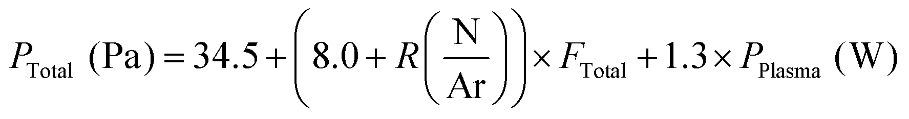
We attribute the increase of the total pressure with plasma power to an increased dissociation of molecules in a more energetic plasma. The interaction between total flow and N/Ar ratio is ascribed to a higher dissociation of N2 at higher total flows, given the higher number of collisions with a higher number of molecules.
Elemental composition and chemical bonding
From ERDA, all deposition conditions resulted in a B content between 37.1 and 43.4 at%, a N content ranging from 27.7 to 42.1 at%, and with a C ranging from 4.8 to 11.6 at%. The hydrogen content in the films was between 3.6 and 5 at%, except for smooth films deposited at low power and high total flow, which contained 7.8 at% H. As all films were subjected to air after the deposition, an O content between 6.6 and 12.9 at% was measured, except for smooth films deposited at low power and high total flow (see below) that displayed up to 20.2 at% O. The measured data was found to be repeatable with the exception of the composition of the films deposited at high total flow, low plasma power and (stray data point in Fig. 2). At these deposition conditions, the carbon and oxygen content of these films was found difficult to evaluate due to the very low density of the films and the uncertainties related to surface contamination. No correlation between the deposition parameters and the atomic composition of the films could be made. The stoichiometries of deposited films are summarized in the ternary diagram in Fig. 2 (red filled circles) and with the compositions compared to selected studies using TBBD (open circles),5 PB (plus signs),5N-TEBA (filled squares),10,11N-TMBA (stars),6,35 TMAB (open triangles),13 B2H6–CH4–N2 mixtures (open squares)36 and BCl3–CH4–N2 mixtures (crosses).37
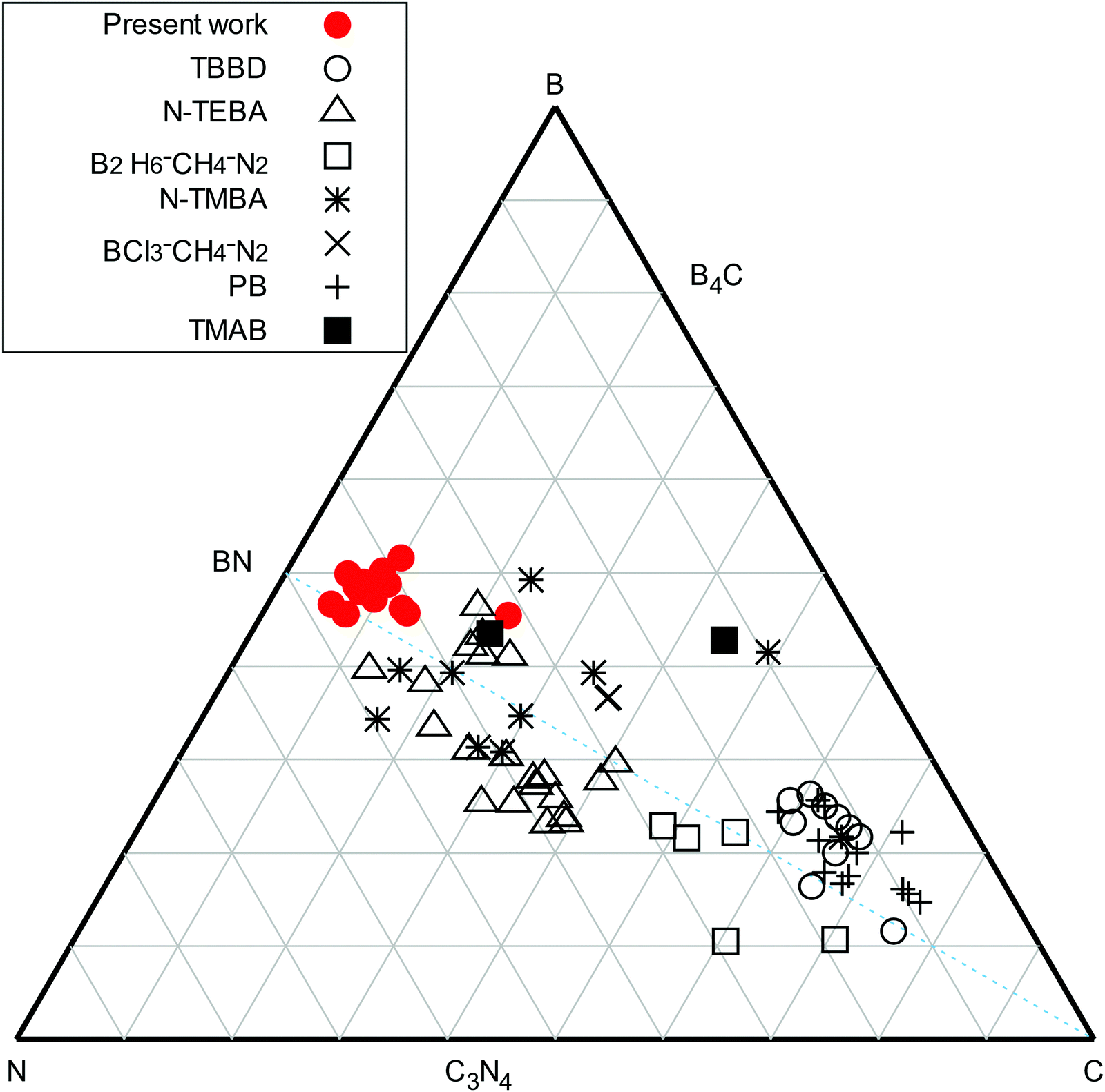 | ||
| Fig. 2 B, C and N content of the deposited films, from ERDA measurements, in this work (red filled circles) compared to previously reported atomic content of plasma CVD B–C–N films deposited below 500 °C, using TBBD (open circles),5 PB (plus signs),5N-TEBA (filled squares),10,11N-TMBA (stars),6,35 TMAB (open triangles),13 B2H6–CH4–N2 mixtures (open squares)36 and BCl3–CH4–N2 mixtures (crosses).37 | ||
From XPS spectra in Fig. 3 it was concluded that B was bonded to N (190.1–190.7 eV38) and C (188.4 eV39) and presented a π-plasmon typical of sp2-hybridized BN at ∼198.5 eV38 (Fig. 3a). The compositional analysis of the XPS spectra showed a higher amount of boron than what can be attributed to the amount of N–B and C–B bonds, which justified the addition of a third component representing B–H bonds around 189 eV.40 N was mainly bonded to B (binding energy of 397.7 eV38) and presented a π-plasmon at ∼406 eV (Fig. 3b), characteristic of sp2-hybridized BN.38 As the optically active species BN,41–44 BN−,45 BNn+ (n = 1, 2, 3)46–48 and BN249 were not detected in the OES spectra (Fig. 1), we speculate that the B–N bonds in the films are formed by surface chemical reactions, alternatively from optically inactive plasma species with B–N bonds. C was bonded to B (282.1 eV39), oxygen (C–O around 286 eV, C![[double bond, length as m-dash]](https://www.rsc.org/images/entities/char_e001.gif) O around 288 eV50) and carbon (284 eV24) (Fig. 3c) and did not present a π-plasmon. The presence of C–C bonds in XPS suggests that at least part of the C2 and CH species, detected by OES (Fig. 1), are incorporated into the film as free carbon.51,52 The absence of C–N bonds in XPS indicates that the CN species detected by OES play a minor role in the film deposition and are pumped out with the gas phase as CN compounds (e.g. CN˙ or HCN).53,54 This is similar to the literature on plasma CVD of diamond,55 carbon nanotubes,56 carbon nitride57 and silicon (oxy)carbonitride.58,59 Thus, the formation of volatile CN compounds could be a carbon sink explaining the high B/C ratios observed in our films compared to films deposited in Ar–TEB plasma.16 The presence of O in the films is believed to be due to exposure to air post deposition. O was found to be mainly bonded to C from the XPS peak around 531 eV (CO bonds), and around 532 eV (O in graphite forming a hydrogen bridge and water) (Fig. 3d).60
O around 288 eV50) and carbon (284 eV24) (Fig. 3c) and did not present a π-plasmon. The presence of C–C bonds in XPS suggests that at least part of the C2 and CH species, detected by OES (Fig. 1), are incorporated into the film as free carbon.51,52 The absence of C–N bonds in XPS indicates that the CN species detected by OES play a minor role in the film deposition and are pumped out with the gas phase as CN compounds (e.g. CN˙ or HCN).53,54 This is similar to the literature on plasma CVD of diamond,55 carbon nanotubes,56 carbon nitride57 and silicon (oxy)carbonitride.58,59 Thus, the formation of volatile CN compounds could be a carbon sink explaining the high B/C ratios observed in our films compared to films deposited in Ar–TEB plasma.16 The presence of O in the films is believed to be due to exposure to air post deposition. O was found to be mainly bonded to C from the XPS peak around 531 eV (CO bonds), and around 532 eV (O in graphite forming a hydrogen bridge and water) (Fig. 3d).60
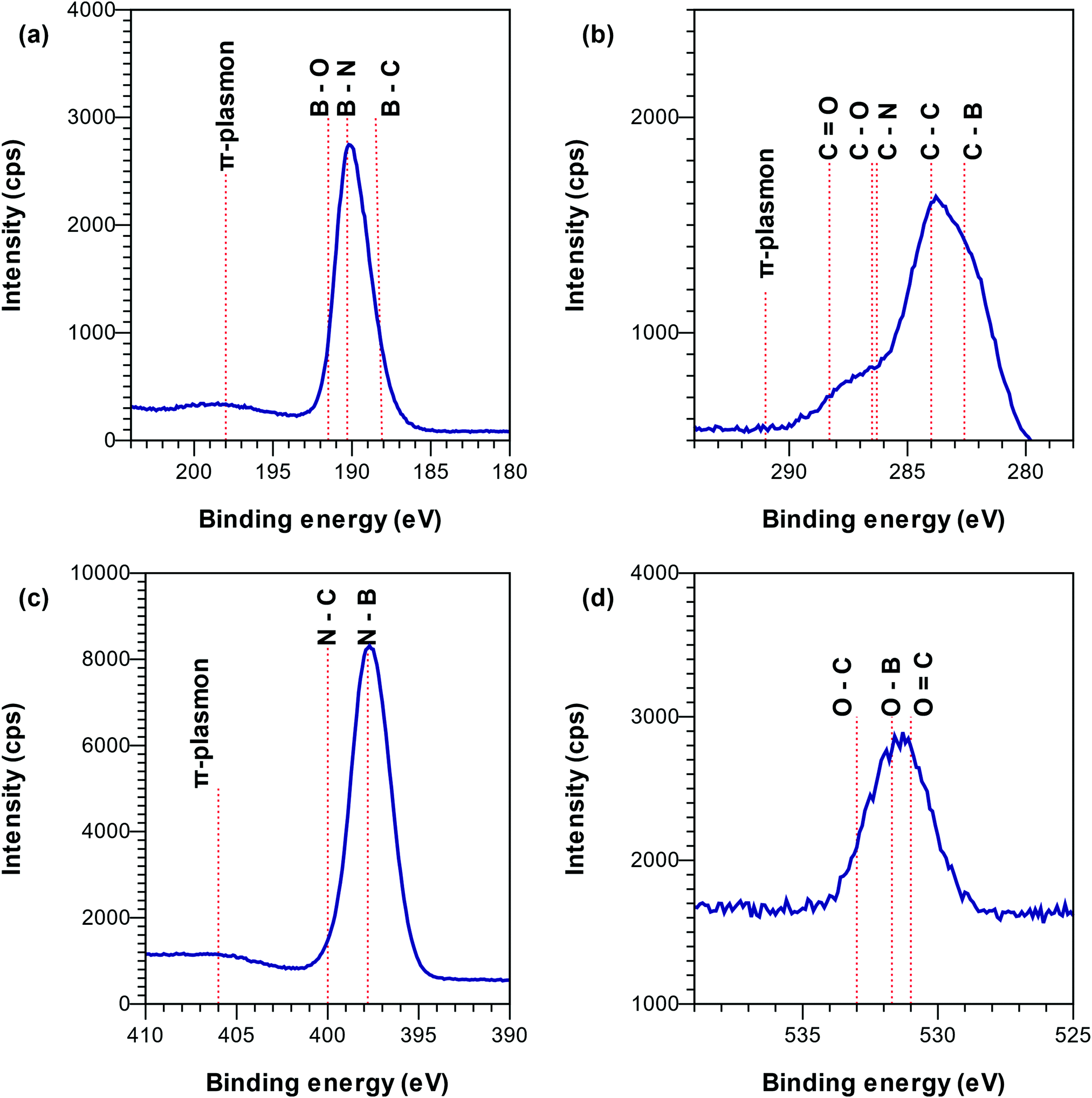 | ||
Fig. 3 High resolution XPS spectra of the B 1s (a), C 1s (b), N 1s (c) and O 1s (d) regions for a sample deposited under 2325 W plasma power, 238 sccm total flow and log(N/Ar) = 1.12 i.e.,  . . | ||
The FTIR reflectance spectra corresponding to the BCN films with different morphologies are presented in Fig. 4. As expected from the composition from ERDA and in agreement with bonding structure obtained from XPS, all the spectra showed the two Reststrahlen bands associated to sp2-BN, albeit slightly shifted towards lower frequencies. The low-density smooth films (smooth 2 in Fig. 4) also presented a broad weak absorption band at 3350 cm−1 associated to N–H bonds. GI-XRD scans obtained from all deposited films revealed no peaks from crystalline phases, suggesting that the films are X-ray amorphous.
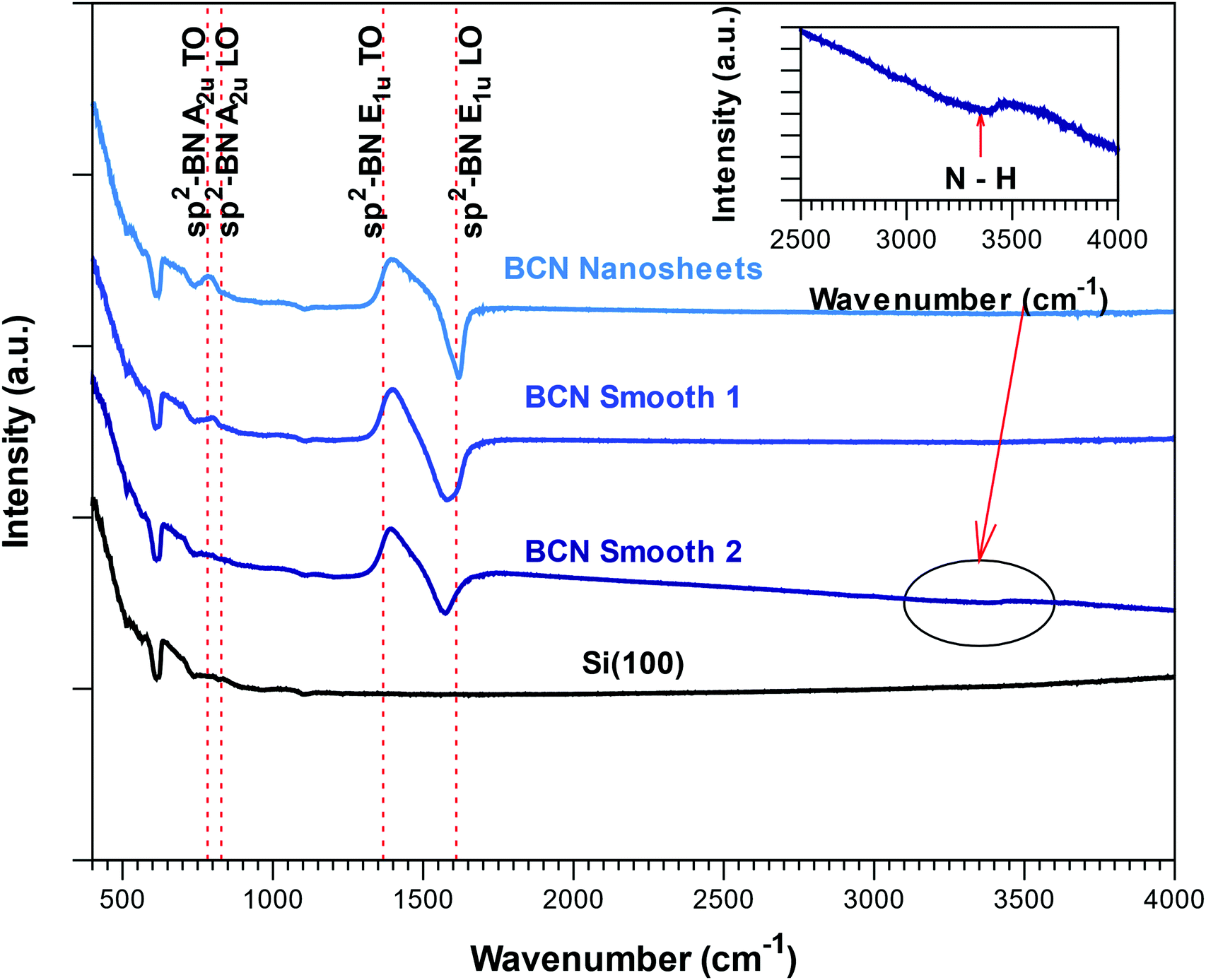 | ||
| Fig. 4 FTIR reflectance spectra of BCN films with different morphologies (see below): nanosheets, dense smooth films (smooth 1) and low-density smooth films (smooth 2). The red dotted lines delimits the Reststrahlen bands of crystalline BN. | ||
Deposition rate and film morphology
The film thickness from SEM cross section images together with their respective deposition times were used to determine the average deposition rate (RD) that was found to be 7 ± 2 nm min−1 in Ar-rich plasmas, independent of both the plasma power and the total gas flow in the chamber. In nitrogen-rich plasmas, the RD was found to increase with increasing total gas flow and to decrease with increasing plasma power. By changing total gas flow and plasma power we have recorded deposition rates between 3 and 63 nm min−1. The deposition rate dependence is summarized as:| RD (nm min−1) = 31.5 + 21.1 × FTotal − 9.4 × PPlasma (W) |
This dependence was validated by depositing a film in nitrogen rich conditions and median power and gas flow, the deposition rate was 34 ± 2 nm min−1 which agrees reasonably well with 31.5 nm min−1 from the above RD dependence on flow and plasma power. We explain the increased deposition rate with higher gas flow to a higher flux of film depositing species at higher gas flow. The decrease in deposition rate with higher plasma power is ascribed to densification of the films due to the increased ion bombardment with higher plasma power, see below.
Furthermore, SEM showed that the films adopt different morphologies depending on the deposition conditions, see Fig. 5a–h. The morphologies alter from smooth films without visible grains at low plasma power, high total flow and high N/Ar, to films of vertically oriented and interconnected nanosheets at low plasma power, low total flow and high N/Ar, to well separated nanosheets with diverse degree of texture and ramification at high plasma power, low total flow and low N/Ar. Deposition of nanosheets have been reported to result in stabilization of sp2-hybridized material by H61 or C262 species in the plasma or by anisotropic etching of sp2-hybridized material along their weekly bonded c-axis.63 The vertical orientation of the sheets is attributed to lateral field effects,61 or crowding62,64 and supported by shadowing of the smaller sheets65 or reinforced by the neighboring sheets.51
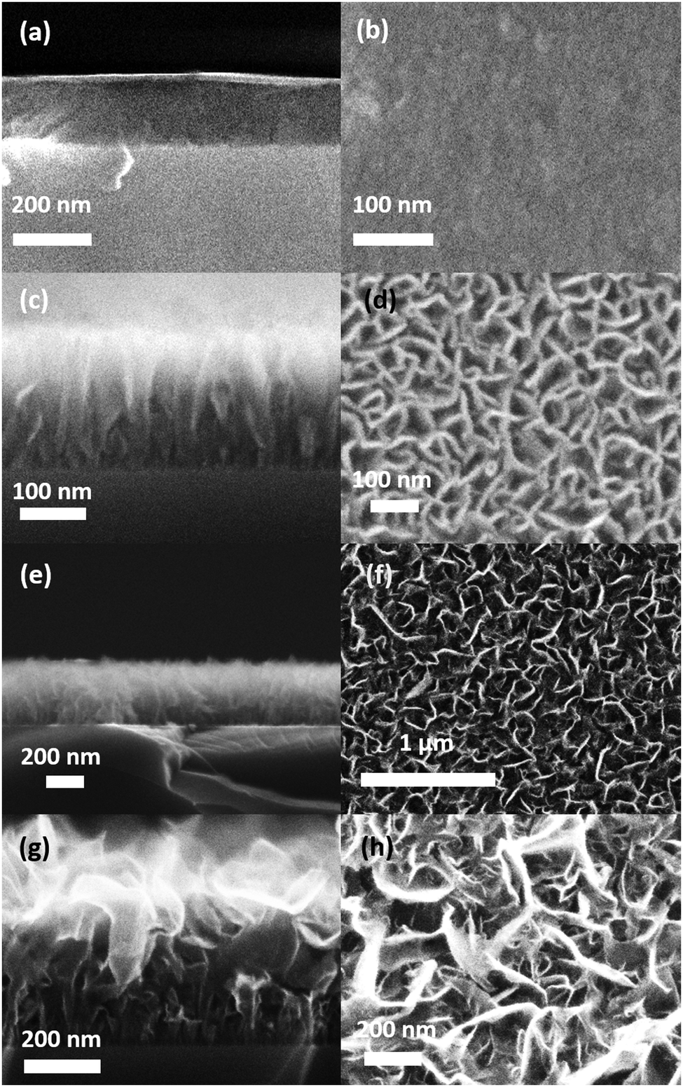 | ||
Fig. 5 Morphology of films deposited under (a and b) 1450 W plasma power, 238 sccm total flow and log(N/Ar) = 1.12 (c and d) 1450 W plasma power, 80 sccm total flow and log(N/Ar) = 1.12 (e and f) 2325 W plasma power, 238 sccm total flow and log(N/Ar) = −1.12 and (g and h) 2325 W plasma power, 80 sccm total flow and log(N/Ar) = −1.12 corresponding to different combinations of  : (a) [−1, 1, 1] (b) [−1, 1, −1] (c) [−1, −1, 1] and (d) [1, −1, −1]. : (a) [−1, 1, 1] (b) [−1, 1, −1] (c) [−1, −1, 1] and (d) [1, −1, −1]. | ||
The evolution of the film nanostructure with the growth parameters is summarized in Fig. 6. Smooth films could be obtained at nitrogen rich plasmas (log(N/Ar) = 1.12), whereas the nanosheet morphologies could be obtained both in argon rich plasmas (log(N/Ar) = −1.12) and in nitrogen rich plasmas (log(N/Ar) = 1.12). The film morphology in nitrogen rich plasmas (log(N/Ar) = 1.12) depends on the interplay between plasma power and total gas flow, as shown in Fig. 6 where two separated regions of the experimental space allow the formation of smooth films. In argon-rich plasmas (log(N/Ar) = −1.12), an increased plasma power leads to less textured morphologies.
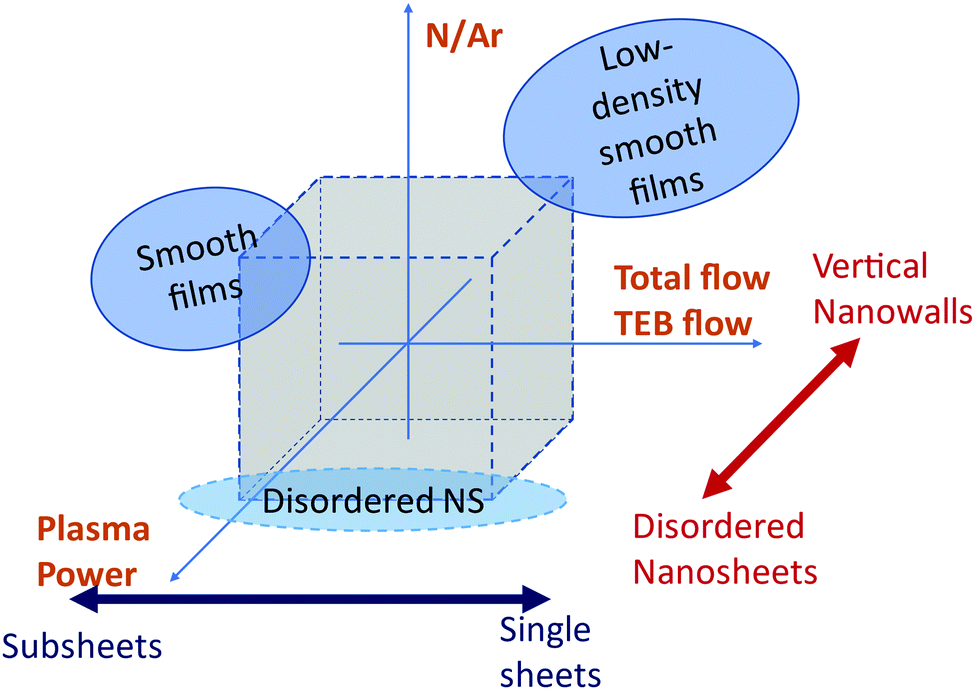 | ||
| Fig. 6 Summary of the dependence of the morphology of the deposited films on the process parameters. | ||
We further note that for a given set of conditions, the morphology of the films becomes less and less oriented with longer deposition time. This is exemplified in Fig. 7 where the film becomes more disordered and show more pronounced sub-sheets with longer deposition time, this behavior is also reported in ref. 66 where BN was deposited by a thermal CVD route using solid boron and ammonia.
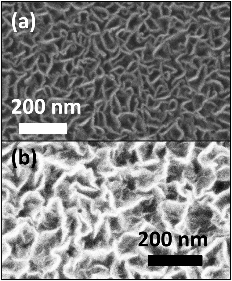 | ||
Fig. 7 (a) Top view SEM of a film deposited under 1450 W, 80 sccm total flow and log(N/Ar) = 1.12 i.e. for 12 min. (b) Top view SEM of a film deposited under the same conditions for 30 min. for 12 min. (b) Top view SEM of a film deposited under the same conditions for 30 min. | ||
Based on ERDA and cross-section SEM, the density of the B–C–N nanosheets was found to be 1.1 ± 0.15 g cm−3, which is lower than the bulk densities of h-BN67(2.18 g cm−3) and B4C68 (2.52 g cm−3), but is consistent with the porous morphology of the films (Fig. 5). The smooth films deposited at high plasma power and low total gas flow had a density of 1.5 ± 0.25 g cm−3 while those deposited at low plasma power and high total gas flow a density of 0.32 ± 0.03 g cm−3.
The observed morphological differences could be explained by ionic bombardment of the films during deposition. The plasma density, i.e. the density of ions in the plasma, will increase with increased plasma power. The ionization potentials for Ar, N2, N and H are 15.76, 15.6, 14.53 and 13.6 eV, respectively.69 But since the cross sections for ionization of these species are 1.6 × 10⁻¹⁶, 9 × 10⁻¹⁷, 1 × 10⁻¹⁶ and 5 × 10⁻¹⁷ cm2 respectively,69 the most likely species to be ionized is Ar, and to some extent N but this first requires the dissociation of N2. Only nanosheets could be deposited in Ar-rich plasmas (Fig. 5 and 6), which could be explained by a too powerful ionic bombardment by Ar+ leading to anisotropic etching of deposited B–C–N material. The high density of the films deposited in nitrogen-rich plasmas at high plasma power and lower flow is explained by (1) the increased mean free path of the ions in the plasma with lower pressure and lower total gas flow, hence more intense ion bombardment and (2) lower amount of Ar+ with respect to other ionic species, in particular from nitrogen, therefore favoring growth over etching. The porosity and morphology of the smooth films with low density is explained by the higher thermal conductivity of nitrogen with respect to argon, resulting in lower growth temperature and deposition in a “hit-and-stick” fashion. This is supported by the high growth rate, high porosity and the presence of N–H bonds which are known to break above 300 °C.70 This is also consistent with the observation of Merenkov et al.71 who reported formation of BN nanosheets from 400 °C and smooth films below 300 °C.
STEM allowed us to obtain some complementary information to SEM by removing the Si substrate. Top-view STEM-HAADF images of the nanosheets show that they are interconnected (Fig. 8(a)), while, as for SEM, cross-section view indicates that the nanosheets are denser close to the substrate and separates along the growth direction (Fig. 8(b)).
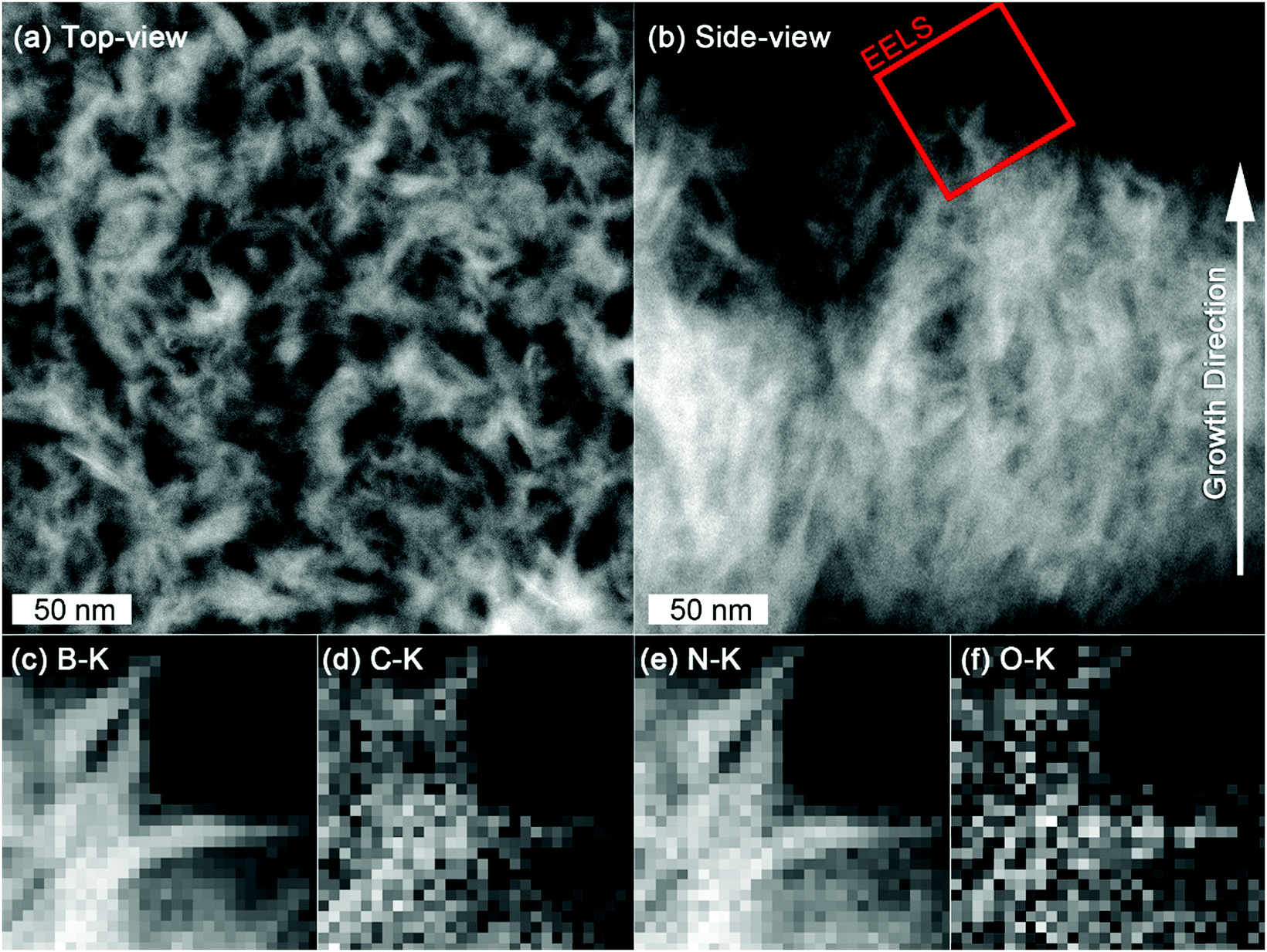 | ||
| Fig. 8 (a) Top-view and (b) cross-sectional view of B–C–N nanosheets by STEM-HAADF imaging (c–f) EELS elemental distribution maps of B (c), C (d), N (e) and O (f) respective K-edges acquired from the area indicated in (b). | ||
While XPS suggested that BN and carbon could potentially form to separate phases, EELS elemental distribution mapping of B, C, N and O (Fig. 8(c)–(f)) revealed the carbon integrity in a BN matrix and that C and O are homogeneously distributed in the B–C–N network.
Electrical measurements.
The relative permittivity (κ) from C–V measurements was shown to span between low-κ and high-κ values (Fig. 9). The smooth B–C–N films showed κ values of 3.3 and 6.3, the lowest value being obtained for the low-density films. The increase of permeability with respect to pure BN can be attributed to an increase in polarizability due to the functionalization of the carbon in the films upon exposure to air. | ||
| Fig. 9 Correlation between the relative permittivity κ of the B–C–N films and argon vapor pressure. Smooth films and nanowalls are represented by full and open circles, respectively. | ||
The films presenting a nanowall structure were found to have κ values as low as 3.4 and as high as 34.8. Since the composition and density of these films are nearly identical, they cannot explain the difference in permittivity, nor can the uncertainties due to the actual contact area on such samples. We suggest that this difference is due to the rigidity of the atomic network, as for a-SixC:H72 and a-BxC:H,73 which in our case could be tuned by Ar ion bombardment. The nanowalls deposited at nitrogen-rich conditions suffer a rather mild bombardment, provided that the Ar partial pressure is low; hence they should have a permittivity in the same range as the smooth films. Conversely, the film deposited in argon-rich conditions suffer a more intense bombardment due to higher impingement flux, resulting in a less dense and more flexible network that can better accommodate the external electric field. This correlation is described in Fig. 9. The permittivity values of our B–C–N films can be compared to κ-values of 1.8–12.8 measured for BxC:H films deposited from TEB by plasma CVD with an Ar plasma.16 The range of κ-values for our B–C–N films is wider than the reported values from films deposited from BCl3–CH4–N2 (1.9–4.2)37,74 and N-TMAB–NH3/H2 (5–9).75 These measurements merit further studies of B–C–N films from TEB in Ar–N2 plasma both for low and high-κ applications.
Conclusions
Plasma CVD with triethylboron and an argon–nitrogen plasma was found to result in the growth of B–C–N films with 37.1 to 43.4 at% B, 27.7 to 42.1 at% N, 4.8 to 11.6 at% C, 3.6 to 7.8 at% H and 6.6 and 20.2 at% O, as seen from ERDA, without clear dependence on the deposition parameters. The films either had a smooth morphology or were constituted of nanowalls. The films were found to be X-ray amorphous with a low density of 1.1 g cm−3 for nanosheets, 1.5 g cm−3 for the denser smooth films and 0.32 g cm−3 for the low-density smooth ones. FTIR and XPS shows that the films comprise predominantly BN in sp2-hybridisation. In addition to this, XPS also shows B–C and C–C bonds. From STEM it is seen that carbon is evenly distributed over the BN matrix. The relatively low amounts of carbon in the films and the absence of C–N bonds is ascribed to production of volatile CN radicals in the plasma, acting as a carbon sink in the deposition chemistry. The dielectric constant of the films was in the range 3.3–35 measured for films and is correlated to the Ar partial pressure and suggested to be explained by structural defects in the films formed by the energetic bombardment.Conflicts of interest
There are no conflicts to declare.Acknowledgements
The authors would like to acknowledge Einar Sveinbjörnsson for assistance with CV measurements. Grzegorz Greczynski, Polla Rouf and Cecilia Goyenola are acknowledged for assistance with the XPS measurements. Babak Bakhit is acknowledged for assistance with ToF-ERDA measurements. This work was supported by the Swedish Foundation for Strategic Research (SSF) (Contract No. IS14-0027). H. P. and H. H. acknowledge financial support from the Swedish Government Strategic Research Area in Materials Science on Advanced Functional Materials at Linköping University (Faculty Grant SFO-Mat-LiU No. 2009-00971). Support from the Swedish research council VR-RFI (Contract 2017-00646_9) for the Accelerator based ion-technological center, and from the Swedish Foundation for Strategic Research (Contract RIF14-0053) for the tandem accelerator laboratory in Uppsala is gratefully acknowledged. The authors acknowledge the Knut and Alice Wallenberg Foundation for support of the Linköping electron microscopy laboratory.Notes and references
- S. W. King, ECS J. Solid State Sci. Technol., 2014, 4, N3029–N3047 CrossRef.
- B. J. Nordell, T. D. Nguyen, C. L. Keck, S. Dhungana, A. N. Caruso, W. A. Lanford, J. T. Gaskins, P. E. Hopkins, D. R. Merrill, D. C. Johnson, L. L. Ross, P. Henry, S. W. King and M. M. Paquette, Adv. Electron. Mater., 2016, 2, 1600073 CrossRef.
- S. Vepřek, Thin Solid Films, 1985, 130, 135–154 CrossRef.
- J. Loeffler, I. Konyashin, J. Bill, H. Uhlig and F. Aldinger, Diamond Relat. Mater., 1997, 6, 608–611 CrossRef CAS.
- D. Hegemann, R. Riedel and C. Oehr, Thin Solid Films, 1999, 339, 154–159 CrossRef CAS.
- S. Stöckel, K. Weise, T. Thamm, K. U. Körner, D. Dietrich and G. Marx, Anal. Bioanal. Chem., 2003, 375, 884–890 CrossRef PubMed.
- T. Thamm, K. U. Körner, W. Bohne, E. Strub, J. Röhrich, S. Stöckel and G. Marx, Appl. Surf. Sci., 2005, 252, 223–226 CrossRef CAS.
- T. Thamm, D. Wett, W. Bohne, E. Strub, J. Röhrich, R. Szargan, G. Marx and W. A. Goedel, Microchim. Acta, 2006, 156, 53–56 CrossRef CAS.
- V. S. Sulyaeva, M. L. Kosinova, Y. M. Rumyantsev, A. N. Golubenko, N. I. Fainer, N. I. Alferova, B. M. Ayupov, P. N. Gevko, V. G. Kesler, B. A. Kolesov, E. A. Maksimovskii, K. G. Myakishev, I. V. Yushina and F. A. Kuznetsov, Inorg. Mater., 2010, 46, 487–494 CrossRef CAS.
- V. S. Sulyaeva, M. L. Kosinova, Y. M. Rumyantsev, V. G. Kesler and F. A. Kuznetsov, Surf. Coat. Technol., 2013, 230, 145–151 CrossRef CAS.
- V. S. Sulyaeva, Y. M. Rumyantsev, V. G. Kesler and M. L. Kosinova, Thin Solid Films, 2015, 581, 59–64 CrossRef CAS.
- M. Abdul Mannan, M. Nagano, T. Kida, N. Hirao and Y. Baba, J. Phys. Chem. Solids, 2009, 70, 20–25 CrossRef CAS.
- M. L. Kosinova, Y. M. Rumyantsev, A. N. Golubenko, N. I. Fainer, B. M. Ayupov, I. P. Dolgovesova, B. A. Kolesov, V. V. Kaichev and F. A. Kuznetsov, Inorg. Mater., 2003, 39, 366–373 CrossRef CAS.
- T. Kida, K. Shigezumi, M. Abdul Mannan, M. Akiyama, Y. Baba and M. Nagano, Vacuum, 2009, 83, 1143–1146 CrossRef CAS.
- T. Sugino and H. Hieda, Diamond Relat. Mater., 2000, 9, 1233–1237 CrossRef CAS.
- M. Imam, C. Höglund, S. Schmidt, R. Hall-wilton, J. Birch and H. Pedersen, J. Chem. Phys., 2018, 148, 034701 CrossRef PubMed.
- J. Uher, S. Pospisil, V. Linhart and M. Schieber, Appl. Phys. Lett., 2007, 90, 2006–2008 CrossRef.
- E. Echeverria, B. Dong, G. Peterson, J. P. Silva, E. R. Wilson, M. S. Driver, Y. S. Jun, G. D. Stucky, S. Knight, T. Hofmann, Z. K. Han, N. Shao, Y. Gao, W. N. Mei, M. Nastasi, P. A. Dowben and J. A. Kelber, J. Phys. D: Appl. Phys., 2016, 49, 355302 CrossRef.
- M. Imam, C. Höglund, J. Jensen, S. Schmidt, I. G. Ivanov, R. Hall-Wilton, J. Birch and H. Pedersen, J. Phys. Chem. C, 2016, 120, 21990–21997 CrossRef CAS.
- B. J. Nordell, C. L. Keck, T. D. Nguyen, A. N. Caruso, S. S. Purohit, W. A. Lanford, D. Dutta, D. Gidley, P. Henry, S. W. King and M. M. Paquette, Mater. Chem. Phys., 2016, 173, 268–284 CrossRef CAS.
- R. Fisher, Statistical Methods for Research Workers, 1925 Search PubMed.
- K. Arstila, J. Julin, M. I. Laitinen, J. Aalto, T. Konu, S. Kärkkäinen, S. Rahkonen, M. Raunio, J. Itkonen, J. Santanen, T. Tuovinen and T. Sajavaara, Nucl. Instrum. Methods Phys. Res., Sect. B, 2014, 331, 34–41 CrossRef CAS.
- S. Hüfner, Photoelectron Spectroscopy: Principles and Applications, Springer-Verlag, Berlin, Germany, 3rd edn, 2010 Search PubMed.
- J. F. Moulder, W. F. Stickle, P. E. Sobol and K. D. Bomben, Handbook of X-ray Photoelectron Spectroscpopy, PerkinElmer Corporation, Eden Prairie, USA, 1992 Search PubMed.
- Ltd. Kratos Analytical Library filename: “casaXPS_KratosAxis-F1s.lib”.
- A. Lofthus and P. H. Krupenie, J. Phys. Chem. Ref. Data, 1977, 6, 113–307 CrossRef CAS.
- S. S. Harilal, R. C. Issac, C. V. Bindhu, V. P. N. Nampoori and C. P. G. Vallabhan, J. Phys. D: Appl. Phys., 1997, 30, 1703–1709 CrossRef CAS.
- J. M. Weinberg, E. S. Fishburne and K. Narahari Rao, J. Mol. Spectrosc., 1967, 22, 406–418 CrossRef CAS.
- A. M. Smith, M. Lorenz, J. Agreiter and V. E. Bondybey, J. Chem. Phys., 1996, 104, 3143–3146 CrossRef.
- M. Wyss, M. Grutter and J. P. Maier, J. Phys. Chem. A, 1998, 102, 9106–9108 CrossRef CAS.
- K. W. Lee and S. J. Harris, Diamond Relat. Mater., 1998, 7, 1539–1543 CrossRef CAS.
- S. Fu, J. Chen, Y. Li, W. Li, M. Zhang and S. Hu, Plasma Sci. Technol., 2008, 10, 70–73 CrossRef CAS.
- T. Ma, H. Liu and Y. Xiong, 2010 Symposium on Photonics and Optoelectronics, 2010, 10–13 Search PubMed.
- P. Tristant, Z. Ding, Q. B. T. Vinh, H. Hidalgo, J. L. Jauberteau, J. Desmaison and C. Dong, Thin Solid Films, 2001, 390, 51–58 CrossRef CAS.
- O. Baake, P. S. Hoffmann, A. Klein, B. Pollakowski, B. Beckhoff, M. L. Kosinova, N. I. Fainer, V. S. Sulyaeva, V. A. Trunova and W. Ensinger, Anal. Bioanal. Chem., 2009, 395, 1901–1909 CrossRef CAS PubMed.
- K. Montasser, S. Hattori and S. Morita, J. Appl. Phys., 1985, 58, 3185–3189 CrossRef CAS.
- T. Sugino, Y. Etou, T. Tai and H. Mori, Appl. Phys. Lett., 2002, 80, 649–651 CrossRef CAS.
- R. Trehan, Y. Lifshitz and J. W. Rabalais, J. Vac. Sci. Technol., A, 1990, 8, 4026–4032 CrossRef CAS.
- T. Shirasaki, A. Derré, M. Ménétrier, A. Tressaud and S. Flandrois, Carbon N. Y., 2000, 38, 1461–1467 CrossRef CAS.
- J. I. Oñate, A. García, V. Bellido and J. L. Viviente, Surf. Coat. Technol., 1991, 49, 548–553 CrossRef.
- A. E. Douglas and G. Herzberg, Can. J. Res., 1940, 18a, 172–185 Search PubMed.
- H. Bredohl, I. Dubois, Y. Houbrechts and P. Nzohabonayo, J. Phys. B: At. Mol. Phys., 1984, 17, 95–98 CrossRef CAS.
- D. Shi, W. Xing, H. Liu, J. Sun, Z. Zhu and Y. Liu, Spectrochim. Acta, Part A, 2012, 93, 367–378 CrossRef CAS PubMed.
- S. Mahmoud, M. Bechelany, P. Miele and M. Korek, J. Quant. Spectrosc. Radiat. Transfer, 2015, 151, 58–66 CrossRef CAS.
- K. R. Asmis, T. R. Taylor and D. M. Neumark, Chem. Phys. Lett., 1998, 295, 75–81 CrossRef CAS.
- R. C. Mawhinney, P. J. Bruna and F. Grein, Chem. Phys., 1995, 199, 163–176 CrossRef CAS.
- R. C. Mawhinney, P. J. Bruna and F. Grein, J. Phys. B: At., Mol. Opt. Phys., 1995, 28, 4015–4025 CrossRef CAS.
- R. C. Mawhinney, P. J. Bruna and F. Grein, J. Chem. Phys., 1995, 103, 8944–8954 CrossRef CAS.
- S. Mahalakshmi and D. L. Yeager, Mol. Phys., 2003, 101, 165–174 CrossRef CAS.
- M. Phaner-Goutorbe, A. Sartre and L. Porte, Microsc., Microanal., Microstruct., 1994, 5, 283–290 CrossRef CAS.
- K. Teii and T. Ikeda, Appl. Phys. Lett., 2007, 90, 88–91 CrossRef.
- K. Tichmann, U. Von Toussaint and W. Jacob, J. Nucl. Mater., 2012, 420, 291–296 CrossRef CAS.
- P. Hammer, M. A. Baker, C. Lenardi and W. Gissler, Thin Solid Films, 1996, 290–291, 107–111 CrossRef CAS.
- F. D. A. Aarão Reis and D. F. Franceschini, Appl. Phys. Lett., 1999, 74, 209–211 CrossRef.
- A. Badzian, T. Badzian and S. T. Lee, Appl. Phys. Lett., 1993, 62, 3432–3434 CrossRef CAS.
- D. B. Hash, M. S. Bell, K. B. K. K. Teo, B. A. Cruden, W. I. Milne and M. Meyyappan, Nanotechnology, 2005, 16, 925–930 CrossRef CAS.
- G. Q. Yu, S. H. Lee, D. G. Lee, H. D. Na, H. S. Park and J. J. Lee, Surf. Coat. Technol., 2002, 154, 68–74 CrossRef CAS.
- M. Belmahi, S. Bulou, A. Thouvenin, L. De Poucques, R. Hugon, L. Le Brizoual, P. Miska, D. Genève, J. L. Vasseur and J. Bougdira, Plasma Processes Polym., 2014, 11, 551–558 CrossRef CAS.
- N. I. Fainer, A. G. Plekhanov, A. N. Golubenko, Y. M. Rumyantsev, E. A. Maksimovskii and V. R. Shayapov, J. Struct. Chem., 2017, 58, 119–125 CrossRef CAS.
- H. Li, Determination of Oxygen Functionality on Highly Oriented Pyrolytic Graphite (HOPG), Doctoral thesis, 2012 Search PubMed.
- Y. Wu, B. Yang, B. Zong, H. Sun, Z. Shen and Y. Feng, J. Mater. Chem., 2004, 14, 469–477 RSC.
- K. Teii, S. Shimada, M. Nakashima and A. T. H. Chuang, J. Appl. Phys., 2009, 106, 084303 CrossRef.
- J. Yu, L. Qin, Y. Hao, S. Kuang, X. Bai, Y. M. Chong, W. Zhang and E. Wang, ACS Nano, 2010, 4, 414–422 CrossRef CAS PubMed.
- A. Malesevic, R. Vitchev, K. Schouteden, A. Volodin, L. Zhang, G. Van Tendeloo, A. Vanhulsel and C. Van Haesendonck, Nanotechnology, 2008, 19, 305604 CrossRef PubMed.
- M. Hiramatsu, K. Shiji, H. Amano and M. Hori, Appl. Phys. Lett., 2004, 84, 4708–4710 CrossRef CAS.
- A. Pakdel, C. Zhi, Y. Bando, T. Nakayama and D. Golberg, ACS Nano, 2011, 5, 6507–6515 CrossRef CAS PubMed.
- O. Madelung, Semiconductor: group IV elements and III–V compound, 1991 Search PubMed.
- O. Knotek, E. Lugscheider and C. W. Siry, Surf. Coat. Technol., 1997, 91, 167–173 CrossRef CAS.
- H. Tawara and T. Kato, At. Data Nucl. Data Tables, 1987, 36, 167–353 CrossRef CAS.
- T. A. Anutgan, M. Anutgan, O. Ozdemir, I. Atilgan and B. Katircioglu, Surf. Coat. Technol., 2008, 202, 3058–3066 CrossRef CAS.
- I. S. Merenkov, M. L. Kosinova and E. A. Maximovskii, Nanotechnology, 2017, 28, 185602 CrossRef PubMed.
- S. W. King, J. Bielefeld, G. Xu, W. A. Lanford, Y. Matsuda, R. H. Dauskardt, N. Kim, D. Hondongwa, L. Olasov, B. Daly, G. Stan, M. Liu, D. Dutta and D. Gidley, J. Non-Cryst. Solids, 2013, 379, 67–79 CrossRef CAS.
- B. J. Nordell, T. D. Nguyen, A. N. Caruso, S. S. Purohit, N. A. Oyler, W. A. Lanford, D. W. Gidley, J. T. Gaskins, P. E. Hopkins, P. Henry, S. W. King and M. M. Paquette, Adv. Electron. Mater., 2017, 3, 1700116 CrossRef.
- S. Umeda, T. Yuki, T. Sugiyama and T. Sugino, Diamond Relat. Mater., 2004, 13, 1135–1138 CrossRef CAS.
- V. S. Sulyaeva, M. L. Kosinova, Y. M. Rumyantsev, F. A. Kuznetsov, V. G. Kesler and V. V. Kirienko, Thin Solid Films, 2014, 558, 112–117 CrossRef CAS.
| This journal is © The Royal Society of Chemistry 2020 |