
 Open Access Article
 This Open Access Article is licensed under a
 Creative Commons Attribution 3.0 Unported Licence
Green and stable processing of organic light-emitting diodes from aqueous nanodispersions†
Anielen H.
Ribeiro
,
Ahmed
Fakih
,
Bas
van der Zee
,
Lothar
Veith
,
Gunnar
Glaser
,
Alexander
Kunz
,
Katharina
Landfester
 ,
Paul W. M.
Blom
and
Jasper J.
Michels
*
,
Paul W. M.
Blom
and
Jasper J.
Michels
*
Max Planck Institute for Polymer Research, Ackermannweg 10, 55128 Mainz, Germany. E-mail: michels@mpip-mainz.mpg.de
First published on 27th March 2020
Abstract
The current factors stopping the up-scaled production of printed thin-film electronics are the flammable and environmentally hazardous solvents used to dissolve the organic semiconductors. Particularly in the case of large-area coating, the development of toxic and flammable vapour during coating and drying poses serious health and safety risks. Processing the active materials from aqueous nanodispersions therefore offers a highly attractive alternative. In contrast to thin-film organic photovoltaics (OPVs), nanoparticle-based organic light-emitting diodes (OLEDs) have so far received little attention. The very high electric field (∼0.1 GV m−1) poses rather “stringent” requirements regarding the topology, integrity and chemistry of the active layer, seemingly difficult to achieve using aqueous nanodispersions. In this work we show that it can be done. We present polymer light-emitting diodes (PLEDs) with active layers processed from nanodispersions. Through thorough optimization of the particle preparation and casting procedures, we obtain smooth, dense and intergral light-emitting nanoparticle films compatible with stable PLED operation. The performance of the nanoparticle PLEDs is on par with that of solution-cast reference devices. The devices exhibit low leakage current and turn-on voltage, no sign of degradation through voltage cycling, no current hysteresis and similar efficiencies.
Introduction
Polymeric semiconductors have attracted considerable attention for application in thin film electronic devices owing to their solubility in organic solvents, ease of processing and compatibility with low cost, scalable manufacture.1 In particular, lighting applications based on polymer light-emitting diode (PLED) technology become feasible when using large area coating methods allowing for drastic cost price-reduction.2 However, a crucial challenge in bringing PLED production from lab to fab is the reduction or elimination of the environmentally hazardous, and often flammable, solvents, such as chloroform, toluene and chlorobenzene, used to dissolve the typical semiconducting polymers that constitute the light-emitting layer.3 As an example, the US Occupational Health and Safety Administration allows for a maximum exposure to chlorobenzene vapour of only 75 ppm for a period of 8 hours. For some EU countries this exposure is even limited to 10 ppm due to possible nephrotoxicity and hepatotoxicity.4A highly attractive alternative fabrication method for polymer electronic devices is, therefore, to process the active material(s) from water, i.e. as an aqueous nanodispersion. This fully eliminates the presence of toxic and flammable fumes during film deposition.5 An accessible and reliable route to synthesize stable aqueous nanodispersions of apolar polymers is mini-emulsification, as introduced by Landfester et al.6 In this process suspended polymer nanoparticles are formed by vigorously stirring an apolar organic solution of the polymer in water in the presence of a, commonly ionic, surfactant that stabilizes the resulting droplets of the polymer solution. The latter subsequently shrink upon slow evaporation of the solvent to give the final dispersion of solid polymer nanoparticles. Of course, the production of dispersions still requires the use of organic solvents, but the fact that now their use is decoupled from large area wet deposition is highly advantageous. Since during mini-emulsification solvent evaporation is much slower, better controlled and not occurring from a large surface area, compliance with safety and health regulations is much more easily achieved in a production environment.7
Besides the environmental and safety benefits, mini-emulsification offers certain advantages in the case of processing blends of multiple polymeric or small molecular functional components: the imposed nano-confinement counteracts the driving force for large scale phase separation resulting from reduced translational entropy and/or repulsive interactions. Irrespective of the miscibility between the blend components, the upper limit for the phase separation length scale is set by the dimensions of the particles.8 For this reason, the use of aqueous nano-dispersions has been widely explored for the manufacture of bulk heterojunction organic photovoltaic (OPV) devices, where the typical length scale of the phase separated donor–acceptor blend is not supposed to exceed the exciton diffusion length of ∼15 nm.3–5,7,9–13 Unfortunately, the performance of these particle-based OPV devices has so far not matched that of their “classical” solvent-processed counterparts, despite decent current–voltage behaviour and low current leakage. Hence, research in this field remains active.
In contrast to OPV, considerably less attention has so far been given to processing the active layers of PLEDs from aqueous nano-dispersions. The reason for this is obvious: when driving a PLED a significantly higher voltage is put across a ∼3 times thinner active layer, in comparison to OPV. Consequently, the electric field at which the devices operate is at least an order of magnitude higher. The resulting high current density hence makes a PLED much more susceptible to electrical breakdown and short circuiting. This imposes tough constraints on both the topological and chemical integrity of the active layer and hence the film forming properties of the nanodispersions. As smooth and integral films are inherently difficult to achieve in a particulate active layer, processing a stably operating PLED from a nanodispersion is much more challenging than an OPV cell. Besides, ionic surfactant residues in the active layer can lead to strongly hysteretic current–voltage (JV) behaviour, which suppresses performance. One study discusses PLEDs prepared from nanodispersions based on the blue emitting ladder-type poly(p-phenylene) polymer MeLPPP.14 However, no information on the leakage current, i.e. a direct measure of the film integrity, or current hysteresis is provided. The reported device efficiency and stability cannot be inferred from the presented data. Besides, the efficiency of the presented devices is comparatively low, as exciton quenching in ladder polymers is substantial due to the high carrier mobility.15
Here, we provide the first detailed study on the fabrication, optimization and characterization of PLEDs, prepared from aqueous nano-dispersions of the poly(p-phenylenevinylene) (PPV)-based polymer emitter poly[2-methoxy-5-(2-ethylhexyloxy)-1,4-phenylenevinylene] (MEH-PPV), blended with polystyrene (PS) to aid film formation. Although the efficiency of our devices seems to be the highest reported so far for organic light-emitting diodes with an active layer processed from a nanodispersion, our main aim is to demonstrate the compatibility between aqueous nanoparticle dispersion technology and the fabrication of stably operating PLEDs. Through optimization of the dispersion, casting and film-forming procedures, we achieve highly integral, smooth and defect-free nanoparticulate light-emitting layers. We confirm the generality of our approach by demonstrating film formation not only for MEH-PPV:PS dispersions, but also for Super Yellow (SY)-PPV:PS nanoparticles. Since the fabrication of PLEDs from aqueous nanodispersions has so far been virtually unexplored, we also provide details on the pitfalls and unexpected observations we encountered during film formation and device optimization. Our final particle-based PLEDs exhibit very low current leakage, low turn-on voltage, non-hysteretic current–voltage characteristics and no sign of degradation upon repeated stress.
Results and discussion
We target smooth and integral active layers for PLED devices, of which the cross-sectional architecture is depicted in Fig. 1a, from aqueous nanoparticle dispersions of MEH-PPV and SY-PPV, blended in a 1![[thin space (1/6-em)]](https://www.rsc.org/images/entities/char_2009.gif) :1 ratio with atactic polystyrene. The choice of these polymeric emitters (molecular structures in Fig. 1b and c) as active materials is fuelled by the fact that they (i) have been well-studied in conventional polymer-based OLEDs,16–20 (ii) are readily available, either via in-house synthesis (MEH-PPV) or through commercial sources (SY-PPV), while showing minimal batch-to-batch variation, (iii) exhibit good to excellent solubility in a range of apolar organic solvents and (iv) pose no intrinsic charge injection barriers, owing to an optimal positioning of the HOMO and LUMO levels relative to the work function of the used electrodes. The HOMO/LUMO levels are (relative to the vacuum level) −5.4/−3.0 eV, and −5.2 eV/−3.0 eV, for SY-PPV19 and MEH-PPV,20 respectively.
:1 ratio with atactic polystyrene. The choice of these polymeric emitters (molecular structures in Fig. 1b and c) as active materials is fuelled by the fact that they (i) have been well-studied in conventional polymer-based OLEDs,16–20 (ii) are readily available, either via in-house synthesis (MEH-PPV) or through commercial sources (SY-PPV), while showing minimal batch-to-batch variation, (iii) exhibit good to excellent solubility in a range of apolar organic solvents and (iv) pose no intrinsic charge injection barriers, owing to an optimal positioning of the HOMO and LUMO levels relative to the work function of the used electrodes. The HOMO/LUMO levels are (relative to the vacuum level) −5.4/−3.0 eV, and −5.2 eV/−3.0 eV, for SY-PPV19 and MEH-PPV,20 respectively.
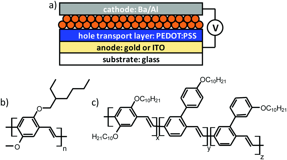 | ||
| Fig. 1 (a) Schematic cross-sectional representation of the architecture of the nanoparticle-based (orange) PLED devices prepared in this work. ITO stands for indium tin oxide. Molecular structures of (b) MEH-PPV and (c) Super Yellow PPV. | ||
The fact that we have gained ample experience with PPV chemistry,21,22 and PLEDs based on PPVs and their blends with other polymers,17,23,24 allows for optimal performance assessment and optimization protocols amenable to future application of more recent and better performing polymers. The blending with polystyrene is performed for reasons of processability: we anticipate that polystyrene acts as a binder, exhibiting modest flow once heated above its glass transition temperature, thereby closing possible cracks left in the nanoparticle films after wet processing. Polystyrene is available in many grades and molecular weights and has a polarity similar to that of PPVs.
Based on recent results,23–25 we anticipate no detrimental effect of the presence of the insulating polystyrene on charge carrier transport, as long as the semiconductor content is kept above ∼10%. We have shown that the transport of positive charge carriers (holes), which dominates the current density in an MEH-PPV-based PLED, in a miscible 1:1 (w/w) blend of MEH-PPV and polystyrene is similar to that in the pure semiconducting polymer (see Fig. 4a in ref. 24). As for the, typically much lower, electron current in MEH-PPV, a modest increase has been observed upon blending with polystyrene, based on the principle of “electron trap-dilution”.23–26 Proving the actual trap-dilution effect requires the study of electron-only devices, which we consider outside the scope of the present work.
The MEH-PPV:PS nanoparticle dispersions are prepared by sonicating an emulsion of a toluene solution of the blend in water, in the presence of the surfactant sodium dodecyl sulfate (SDS). For SY-PPV:PS nanoparticle dispersions, chloroform is used as the solvent. Upon evaporation of the solvent, the droplets solidify and transform into solid polymer blend nanoparticles. For a detailed description of the nanoparticle synthesis we refer to the Experimental section. SDS is highly attractive from the point of view of obtaining stable nanodispersions, but the use of this ionic species poses a fundamental challenge if it becomes incorporated in the emitting layer of a PLED. As is well known from studies on light-emitting electrochemical cells (LEECs),27 and hybrid metal–organic devices,28 since mobile ionic species typically exhibit much slower transport than the electronic charge carriers, their presence can lead to considerable performance loss associated with hysteretic JV behaviour. Naturally, one could instead use a non-ionic surfactant in the manufacture of the nanodispersion. However, we refrain from doing so due to the fact that these are significantly less effective in stabilizing the emulsion droplets and the final solid particles.29
After emulsification and solvent evaporation, we removed the excess of SDS by extensive dialysis30 (see Experimental section). Optimal PLED operation would require removing as much SDS as possible, i.e. by applying long dialysis times. On the other hand, removal of too much SDS destabilizes the nanoparticle dispersion and compromises its processability due to a rise in surface tension. In relation to this, Bag et al.4 and Janssen et al.12 also observed that, in the case of polymer:PCBM nanodispersions, a too high concentration of SDS may lead to the formation of holes in the films due to dewetting. In order to arrive at an optimal SDS concentration, we monitor the surface tension of the dispersion, and the equilibrium (ionic) conductivity of the receiving phase (see Experimental section for details), as a function of dialysis time. Fig. 2 shows the corresponding curves for the SY-PPV:PS nanodispersion, the trends of MEH-PPV:PS being highly similar.
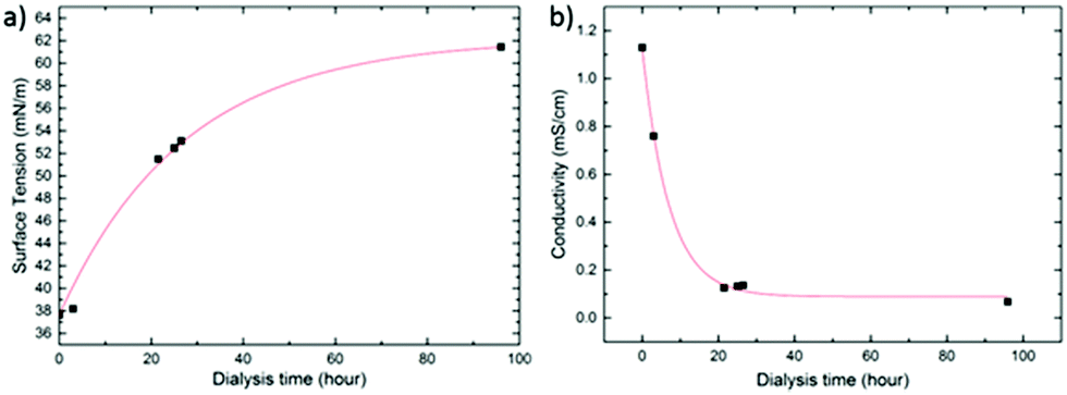 | ||
| Fig. 2 (a) Surface tension and (b) receiving phase conductivity as a function of dialysis time for a dispersion of SY-PPV:PS as a representative example. The red curves are guides for the eye. | ||
As revealed by Fig. 2a, the surface tension increases sub-linearly from ∼38 to ∼60 mN m−1 over the course of 96 h. Interestingly, the conductivity of the dialysis medium drops steeply within the first 20 h and levels off at ∼0.15 S cm−1 despite the ongoing rise in surface tension. This demonstrates that beyond this point the free surfactant concentration is very low, probably lower than the critical micelle concentration (CMC), though still high enough to give surface tension significantly lower than that of pure water (i.e. 72 mN m−1). Moreover, the fact that even after 96 h of dialysis time no nanoparticle agglomeration is observed shows that the density of bound SDS remains sufficiently high for the dispersion to remain stable. This may indicate that SDS molecules become kinetically trapped in the glassy polymer matrix during the final stages of solvent evaporation. We find a surface tension of the dispersion of around 60 mN m−1 to be an ideal compromise between stability, good wetting behaviour and, as shown below, minimal current–voltage hysteresis.
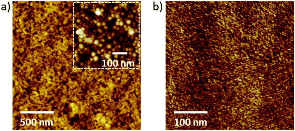
In the final step of the nanoparticle synthesis we concentrate the dispersions to a total solids content of 6 wt% by centrifugation and subsequent decantation of the supernatant. In agreement with observations by Janssen et al.12 we find that concentrated dispersions exhibit improved film formation in comparison to dilute dispersions. The resulting particle diameters are respectively: ![[d with combining macron]](https://www.rsc.org/images/entities/i_char_0064_0304.gif) = 65 ± 30 nm and = 125 ± 40 nm, as determined by DLS (see Experimental section). These numbers are in qualitative agreement with high-magnification top view SEM analysis (Fig. 3) of nanoparticle films, cast onto glass slides coated with PEDOT:PSS, i.e. the hole injecting material in the final PLED devices and relevant substrate for the emitting layer (see Fig. 1a).
= 65 ± 30 nm and = 125 ± 40 nm, as determined by DLS (see Experimental section). These numbers are in qualitative agreement with high-magnification top view SEM analysis (Fig. 3) of nanoparticle films, cast onto glass slides coated with PEDOT:PSS, i.e. the hole injecting material in the final PLED devices and relevant substrate for the emitting layer (see Fig. 1a).
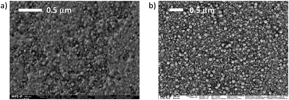 | ||
| Fig. 3 High magnification top view SEM images of (a) MEH-PPV:PS and (b) SY-PPV:PS nanoparticle films cast onto PEDOT:PSS-covered glass slides. | ||
As mentioned in the introduction, a major challenge associated with preparing PLEDs from aqueous nano-dispersions is to obtain smooth and functional layers of the semiconducting nanoparticles, with a suitable thickness and very low defect density at large length scales. An active layer containing cracks and holes leads to undesired current pathways between the cathode and anode, resulting in a high leakage current and short-circuits.31,32 Furthermore, it should be realized that due to the finite size of the particles, the exact thickness of the active layer may be difficult to control. Hence, prior to fabricating the devices, we investigate film formation during casting, this time using PEDOT:PSS-anode-glass substrates to also study the possible influence of the anode material. Subjecting the PEDOT:PSS substrates to hard baking and a subsequent mild nitrogen plasma treatment (see Experimental section) prior to casting the aqueous dispersions proves essential in obtaining good wetting, while increasing the resilience of the relatively hydrophilic PEDOT:PSS against dissolution.
In agreement with Stapleton et al.,33 we observe a strong reduction in the defect density of the particle films upon casting the nanodispersions in multiple consecutive casting steps: typically three for SY-PPV:PS and two for MEH-PPV:PS, each pass preceded by a nitrogen plasma pretreatment to preserve wettability. Typically, we subject the final nanoparticle films to mild annealing at 110 °C for 2 h. Interestingly, the nature of the anode material below the PEDOT:PSS layer influences the integrity of the nanoparticle films. When using 20 nm of gold (nominally) as a transparent anode, applied by thermal evaporation, we observe a morphology comprising closely packed nanoparticles (see Fig. 3 above and Fig. S1a in the ESI†).
Besides details on the level of single nanoparticles, i.e. convenient for size determination as outlined above, the SEM images give an impression of the general integrity of spin-coated particle films. An important observation is that macroscopic cracks and voids are absent. The particle layers are devoid of macroscopic defects across a surface area of at least multiple hundreds of square micrometers (see ESI,† Fig. S1a). The smaller dark areas discernible between the particles (Fig. 3) likely represent lower-lying regions in the film. It is hard to say whether these regions progress all the way through the layer or merely represent dimples. The fact that the leakage current in nanoparticle-based PLEDs is comparable to that of solution-cast devices, as we show below, strongly supports the notion that a substantial fraction of the dark areas indeed represent dimples rather than true holes or punctures. What is more, as we discuss below and in Section S4 of the ESI,† films of polystyrene-free nanoparticles do show an elevated density of true holes and punctures.
Interestingly, with the same pretreatment and casting procedure though using indium tin oxide (ITO) as the anode, we obtain a characteristic pattern comprising undesirable “horseshoe”-shaped dimples in the nanoparticle films (see ESI,† Fig. S1b). We speculate that ITO affects the homogeneity of the nitrogen plasma during pretreatment, leaving distinct areas on the surface untreated. Since the aim of this work is to demonstrate properly functioning PLEDs based on smooth, defect-free light-emitting nanoparticle films, we base our actual devices on a transparent gold anode, rather than ITO.
Since the use of multiple coating passes poses the risk that the active layer becomes too thick (i.e. significantly exceeding 100 nm), especially if the particle diameter is large, we proceed with PLED device preparation using only the smaller (65 nm) MEH-PPV:PS particles. We also note that in this respect nanoparticle-based PLEDs are arguably more challenging than OPV devices, since for the latter the optimum film thickness is significantly higher (typically a few hundred nanometers). As mentioned above, the MEH-PPV:PS dispersion requires only two coating passes to yield a smooth and integral nanoparticle film. To visualize the topological and morphological characteristics of the combined organic stack, we subject the MEH-PPV:PS films on PEDOT:PSS to cross-sectional SEM analysis (Fig. 4). The cross-section has been obtained by freeze-fracture.
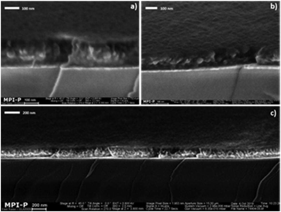 | ||
| Fig. 4 Cross-sectional SEM images at decreasing magnification (a)–(c) of an MEH-PPV:PS nanoparticle film on glass-Au-PEDOT:PSS, obtained after two consecutive spin-coating passes and subsequent annealing at 110 °C for 2 h. | ||
The images show a smooth film containing closely packed nanoparticles with homogeneous thickness (measured to be 140 nm by profilometry). The gold anode is marked by the thin “white” film, clearly visible on top of the extended dark region representing the glass substrate. Unfortunately, the PEDOT:PSS layer is not clearly discernible, possibly due to the edge serrations induced by the film-fracture process. Hence, the cross-sectional SEM analysis does not confirm that the PEDOT:PSS indeed survives the repeated casting of the aqueous nanodispersion.
For this reason, we analysed the composition of the combined organic stack using secondary ion mass spectrometry (SIMS) depth profiling. The raw ion traces are depicted in Fig. S2 of the ESI.† Various ionic fragments have been detected that can be assigned to the individual components in the stack (see Table S1, ESI†). Importantly, the SIMS analysis unambiguously demonstrates that, although not clearly visible in cross-sectional SEM images, there is a well-defined interface between the particulate PPV:PS-rich and PEDOT:PSS-rich regions in the stack (see Section S2 of the ESI† for a detailed argumentation). Based on the individual sputtering yields of PPV:PS and PEDOT:PSS, and the measured total thickness of 140 nm, we estimate the PPV:PS-rich and PEDOT:PSS-rich regions to have thicknesses of ∼85 and ∼55 nm, respectively. The fact that the latter excellently agrees with the thickness of the pristine PEDOT:PSS layer (see Experimental section) demonstrates that the hole-injection layer film is fully unaffected by the casting of the aqueous dispersion. This confirms the robustness of our processing procedure. Although the numbers are certainly subject to some error, the 85 nm for the PPV:PS-rich region shows that the two coating passes do not result in a cumulative value of twice the mean particle diameter.
Although we consider an extensive discussion of the SIMS analysis outside the scope of this work, some notable observations should be mentioned. First, a minor fraction of PSS seems to be present in the upper region of the stack (indicated by the dark blue, green and red traces in Fig. S2, ESI†), likely due to swelling of the PEDOT:PSS layer during casting of the aqueous dispersion. Vice versa, the magenta trace in Fig. S2b (ESI†) suggests that a minor fraction of the PPV:PS nanoparticles protrude into the lower lying region of the stack. This may be a result of the softening of the PEDOT:PSS due to water-ingress. Furthermore, the molecular ion of SDS is encountered predominantly in the top-most region, which is perhaps not surprising due to its surface active properties.
As a last step in our thin-film characterization, prior to studying the actual PLEDs, we investigate the surface properties of the MEH-PPV:PS nanoparticle films using atomic force microscopy (AFM) and compare the results with the solvent-cast reference layers (see Fig. 5). Fig. 5a and b represent a topography scan (a) and a peak force measurement (b) of an MEH-PPV:PS nanoparticle film annealed at 110 °C (a), and a drop-cast MEH-PPV:PS nanoparticle film which underwent FIB-polishing to expose the interior of the particles. From image (5a) we infer a root-mean-square roughness of ∼4 nm, i.e. considerably less than the dimensions of the particles themselves (see inset of Fig. 5a) and in qualitative agreement with cross-sectional SEM analysis (Fig. 4). The absence of spatial inhomogeneity in the peak-force measurement (5b) demonstrates that (large scale) phase separation between the PPV and polystyrene is fully suppressed by the nano-confinement.
 | ||
| Fig. 5 AFM topography image of (a) an MEH-PPV:PS nanoparticle film on Au-PEDOT:PSS, obtained after two consecutive spin-coating passes and annealed at 110 °C for 2 h, and (b) AFM peak-force measurement of an FIB-polished region of a drop-cast MEH-PPV:PS nanoparticle film. The inset in (a) represents a magnification. | ||
In what follows we present the optoelectrical characterization and performance of the MEH-PPV:PS nanoparticle-based PLEDs, in comparison to reference devices based on the solution-cast blend. PLEDs are obtained by applying barium-aluminum cathodes directly onto the nanodispersion- or solution-cast active layer (see Fig. 1a) by vapour deposition. Subsequently, the devices are subjected to voltage sweeps during which we record the current flowing through the devices, and the wavelength and intensity of the electroluminescence (EL). Fig. 6 shows a representative EL spectrum recorded for the MEH-PPV:PS nanoparticle-based PLEDs (red), together with the spectrum of the reference device (black). The fact that the EL spectra of the nanoparticle-based and reference devices are relatively similar demonstrates that the nanoconfinement of the chromophores does not affect their spectral properties in comparison to those of the solution-cast polymer.
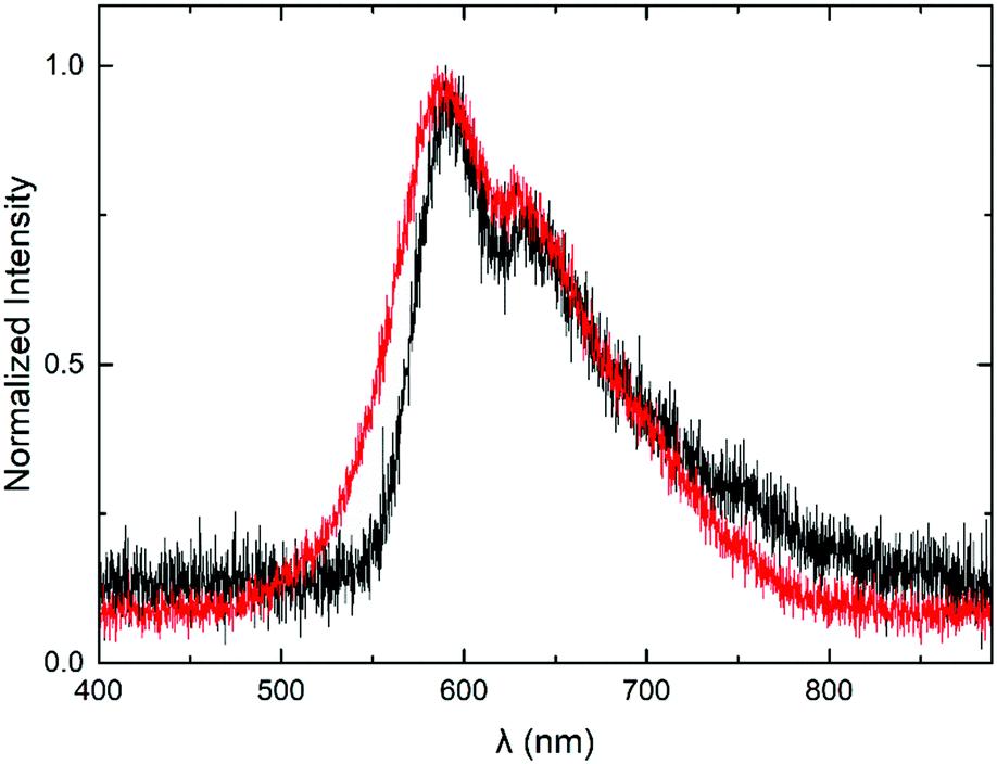 | ||
| Fig. 6 Electroluminescence emission spectra of an MEH-PPV:PS nanoparticle-based PLED (red) and a reference device based on the solution-cast MEH-PPV:PS blend. | ||
Fig. 7a shows the current density and luminancea,b (cd m−2) of the MEH-PPV:PS nanoparticle (red) and solution-cast reference devices (black) as a function of the applied voltage. The corresponding current efficiencies (cd A−1) are plotted as a function of the applied voltage in Fig. 7b. The solid, dashed and dashed-dotted lines represent consecutive bias scans. The fact that they coincide in all the cases demonstrates the absence of performance loss upon repeated stress. This confirms the operational stability of both the nanoparticle-based and reference PLEDs.
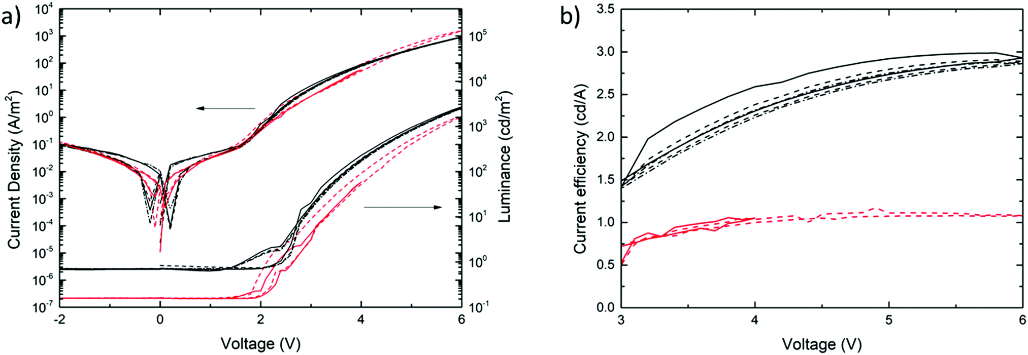 | ||
| Fig. 7 (a) Current density (J) (left y-axis) and luminance (right y-axis), plotted as a function of applied voltage (V) for an MEH-PPV:polystyrene nanoparticle PLED with a 85 nm thick active layer (red) and a solution-cast MEH-PPV:polystyrene reference device with a 90 nm active layer (black). (b) Current efficiencies of the MEH-PPV:polystyrene nanoparticle (red) and reference (black) devices, plotted as a function of voltage. Solid, dashed and dashed-dotted lines represent consecutive voltage scans. All curves have been measured at 295 K. | ||
Fig. 7a shows that the current–voltage characteristics of the aqueous-processed MEH-PPV:PS nanoparticle PLEDs equal those of devices based on solution-cast active layers with, in this case, a thickness of 90 nm. The fact that the curves coincide across the scanned voltage range confirms that charge injection and transport is neither compromised by the nanoparticulate nature of the active layer, nor by chemical residues that remain from the nanoparticle synthesis, such as the surfactant. This result also shows that charge blocking or trapping is not significantly more pronounced in the particle-based device in comparison to that in the solution-processed reference PLEDs.
First, the fact that for |V| < 2 V the particle-based PLEDs exhibit the same low leakage current as that measured for the reference devices confirms the high film quality of the former. Second, the similar turn-on voltage and current increase at V ≈ 2 V demonstrate fully efficient charge injection and transport. Third, despite the use of SDS as an anionic surfactant in the nanoparticle synthesis, the absence of current hysteresis in the nanoparticle PLEDs shows that there are no losses due to ionic transport, even in the (typically) high electric field. This suggests that the residual amount of surfactant is very low and/or that transport of SDS is considerably slowed down in the glassy polymer film.
In addition, we prepare PLEDs based on unblended MEH-PPV nanoparticles to demonstrate the benefits of polystyrene to improving the film integrity and suppressing the leakage currents. These results, which are included in Section S4 of the ESI,† indeed suggest that the addition of polystyrene is beneficial for obtaining a high film integrity. In general, active layers prepared from PS-free nanoparticles show an elevated defect density, likely due to a reduced healing of processing-related cracks during the annealing step. For further details we refer to Section S4 of the ESI.†
Despite the very similar current–voltage behaviour, the luminance curves (Fig. 7a) reveal a modest efficiency-loss of the nanoparticle-based PLED in comparison to the solution-processed reference device. As a result, the luminous efficiency of the particle-based device turns out to be about a factor of 2.5 lower than that of the reference PLED, as expressed by the curves in Fig. 7b. Since this relative loss cannot be explained by compromised charge carrier transport, we propose that optical losses are enhanced in the nanoparticle-based device. Assuming the particle size of d = 65 ± 35 nm not to change significantly after processing, we find the length ratio α = πd/λ to be in the range 0.2–0.5, with λ = 600 nm (based on Fig. 6). This value is consistent with the upper and lower ranges of, respectively, the Raleigh and Mie scattering regimes. Since we measured the light only in the out-of-plane direction, rather than using an integrating sphere, we suspect enhanced scattering to be accountable for the efficiency loss.
Conclusions
In summary, in this work we prepare polymer light-emitting diodes with active layers comprising electroluminescent nanoparticles of MEH-PPV:PS blends, processed from aqueous dispersions. We optimize our nanoparticle preparation and film casting procedures, in order to meet the stringent topological and chemical film quality prerequisites associated with stably functioning PLED devices. The dispersions are fabricated using the mini-emulsion method and dialyzed to reduce the surfactant (SDS) concentration as much as possible, while retaining stability. We obtain defect-free and smooth thin films of light-emitting nanoparticles on the commonly used hole injection material PEDOT:PSS via a multistep casting procedure involving repeated plasma treatment for good wetting behaviour. Interestingly, the quality of the film depends on the nature of the anode material below the PEDOT:PSS. Near perfect nanoparticle layers are obtained in the case of a transparent gold anode, whereas ITO leads to microscopic wetting defects in the nanoparticle layer.Top-view and cross-sectional microscopic analysis confirms the topological film quality. Chemical depth-profiling demonstrates that a “hard-bake” procedure makes the relatively hydrophilic PEDOT:PSS layer fully resilient against dissolution during casting of the aqueous dispersion. The performance of the final nanoparticle-based PLEDs is stable across multiple voltage scanning cycles and their efficiencies are on par with those of reference devices with solution-cast active layers. The fact that our PPV:PS nanoparticle-based PLEDs and the reference devices show highly similar current–voltage characteristics, including a low leakage current, low turn-on voltage and no hysteresis, confirms that we have overcome the most important challenges associated with the fabrication of PLEDs based on a nanoparticulate active layer. Hence, with this work we demonstrate aqueous nano-dispersion technology to be fully compatible with safe and green PLED manufacture.
Experimental
Materials
MEH-PPV34 (Mn = 70000 g mol−1, Mw = 250000 g mol−1, Đ = 3.57) and polystyrene (atactic, Mn = 88000 g mol−1, Mw = 92000 g mol−1, Đ = 1.05) were synthesized in house. Super Yellow (SY) –PPV (Mn > 400000 g mol−1, Mw > 1300000 g mol−1, Đ ≈ 3) and sodium dodecyl sulfate (SDS, purity >99%) were purchased from Sigma-Aldrich and used as received. Chloroform (purity ≥ 99.8%) and toluene (purity ≥ 99.8%) were purchased from Fisher Chemical and used as received.
Synthesis of aqueous polymer blend dispersions
Aqueous PPV:PS blend (1:1 w/w) nanoparticle dispersions were synthesized following the procedure developed by Landfester et al.6 50 mg of PPV and 50 mg of polystyrene were dissolved in 4 mL of chloroform (SY-PPV:PS) or toluene (MEH-PPV:PS) to obtain a 25 mg mL−1 total solids concentration. The polymer blend solution was passed through a 5.0 μm PTFE filter and added dropwise to 10 mL of a stirred 1.5 wt% SDS solution in deionized water. The solution was kept stirring for one hour for pre-emulsification. The mini-emulsion was prepared by subsequently sonicating the mixture for 6 min at 70% amplitude using a Branson sonifier W450 equipped with a 1/2” tip. The sample was stirred overnight at room temperature to evaporate the chloroform or at 80 °C for 3 days to evaporate the toluene. The dispersion was dialyzed (VISKING dialysis tubing, regenerated cellulose, and diameter 21 mm) in deionized water (Direct-Q3 UV-R, 18.2 MΩ cm, Merck) until its surface tension reached the range of 50–60 mN m−1 (Dataphysics DCAT 21 tensiometer). Finally, the sample was concentrated by centrifugation (Sigma 3-30KS) to 6 wt% solids by using a centrifugal filter (Amicon Ultra-100K, Merck) and subsequently filtrated through a 0.5 μm PTFE filter.
Substrate preparation and particle film casting
Glass and glass-ITO (indium tin oxide) substrates were cleaned using a detergent solution and subsequent rinsing with deionized water, acetone and isopropanol. To fabricate transparent gold electrodes, a 1 nm layer of Cr was thermally evaporated at 10−7 mbar directly onto glass substrates, followed by evaporation of a, nominal, 20 nm gold layer. The glass-ITO and glass-Au substrates received a 20 min UV–ozone treatment, after which a 55 nm layer of the hole injection material poly(3,4-ethylenedioxythiophene):poly(styrene sulfonate) (PEDOT:PSS, Heraeus Clevios 4083) was applied by spin-coating and subsequently baked at 200 °C for 1 h. Prior to casting the PPV:PS nanoparticles from the aqueous dispersion, the PEDOT:PSS surface was subjected to a nitrogen plasma treatment (5 s, 100 W). Nanoparticle films were prepared by repeated casting of a 6 wt% PPV:PS dispersion, drying at 70 °C for 5 min and a nitrogen plasma treatment (5 s, 100 W).Dispersion and film characterization
The size and distribution of the polymer blend particles were measured by means of dynamic light scattering (DLS) at a fixed scattering angle of 90° using a Zetasizer Nano S90. Scanning electron microscopy (ZEISS 1530 Gemini, Carl Zeiss Microscope GmbH operating at 0.1 kV) was performed to further study the particle size and particle film morphology. Tapping-mode atomic force microscopy (AFM) was carried out using a Bruker Dimension Icon FS.PLED fabrication and characterization
The as prepared MEH-PPV:PS stacks were annealed at 110 °C for 2 h under an inert atmosphere, after which a Ba/Al (5 nm/100 nm) cathode was thermally evaporated. For the reference devices, a solution of MEH-PPV:PS (1:1 w/w) in toluene was spin-coated onto the treated PEDOT:PSS substrates and subjected to the same annealing treatment as the nanoparticle devices. JV measurements were obtained using a Keithley 2400 source unit, and the light output was measured using a photodiode connected to a Keithley 6514 electrometer. The electroluminescence data were recorded using an Ocean Optics USB2000 spectrometer. The area of each pixel is 1 mm2.
Notes
(a) All luminance values have been corrected for the fact that a 20 nm gold layer as the anode reduces the transparency of the device by about a factor of three in comparison to a PLED based on the more commonly used ITO (see ESI†).(b) The difference in baseline elevation of the luminance-vs.-voltage curves in Fig. 7a is due to a difference in ambient lighting during the measurements (the measurements have taken place on different days, characterized by different environmental lighting conditions). For voltages exceeding 2.5 V, i.e. the window relevant to assessing device operation, the luminance increases by several orders of magnitude. Hence, in this regime, the contribution of ambient lighting to the measured photocurrent (from which the luminance has been derived) can be considered negligible.
Conflicts of interest
There are no conflicts to declare.Acknowledgements
Open Access funding provided by the Max Planck Society.Notes and references
-
K. Wiesenhütter and W. Skorupa, Low-Cost and Large-Area Electronics, Roll-to-Roll Processing and Beyond, ed. W. Skorupa and H. Schmidt, Subsecond Annealing of Advanced Materials, Springer Series in Materials Science, Springer, Cham, 2014, vol. 192 Search PubMed
.
- D. Wang, J. Hauptmann and C. May, MRS Adv., 2019, 4, 1367–1375 CrossRef
- L. D'Olieslaeger, G. Pirotte, I. Cardinaletti, J. D'Haen, J. Manca, D. Vanderzande, W. Maes and A. Ethirajan, Org. Electron., 2017, 42, 42–46 CrossRef
- M. Bag, T. S. Gehan, L. A. Renna, D. D. Algaier, P. M. Lahtia and D. Venkataraman, RSC Adv., 2014, 4, 45325–45331 RSC
- E. B. L. Pedersen, M. C. Pedersen, S. B. Simons, R. G. Brandt, A. P. L. Böttiger, T. R. Andersen, W. Jiang, Z. Y. Xie, F. C. Krebs, L. Arleth and J. W. Andreasen, J. Mater. Chem. A, 2015, 3, 17022–17031 RSC
- K. Landfester, Adv. Mater., 2001, 13, 765–768 CrossRef CAS
- L. D’Olieslaeger, M. Pfannmöller, E. Fron, I. Cardinaletti, M. Van Der Auweraer, G. Van Tendeloo, S. Bals, W. Maes, D. Vanderzande, J. Manca and A. Ethirajan, Sol. Energy Mater. Sol. Cells, 2017, 159, 179–188 CrossRef
- T. Kietzke, D. Neher, K. Landfester, R. Montenegro, R. Güntner and U. Scherf, Nat. Mater., 2003, 2, 408–412 CrossRef CAS PubMed
- T. Kietzke, D. Neher, M. Kumke, R. Montenegro, K. Landfester and U. Scherf, Macromolecules, 2004, 37, 4882–4890 CrossRef CAS
- N. P. Holmes, N. Nicolaidis, K. Feron, M. Barr, K. B. Burke, M. Al-Mudhaffer, P. Sista, A. L. D. Kilcoyne, M. C. Stefan, X. Zhou, P. C. Dastoor and W. J. Belcher, Sol. Energy Mater. Sol. Cells, 2015, 140, 412–421 CrossRef CAS
- N. P. Holmes, M. Marks, P. Kumar, R. Kroon, M. G. Barr, N. Nicolaidis, K. Feron, A. Pivrikas, A. Fahy, A. Diaz de Zerio Mendaza, L. D. Kilcoyne, C. Müller, X. Zhou, M. R. Andersson, P. C. Dastoor and W. J. Belcher, Nano Energy, 2016, 19, 495–510 CrossRef CAS
- F. J. Colberts, M. M. Wienk and R. A. J. Janssen, ACS Appl. Mater. Interfaces, 2017, 9, 13380–13389 CrossRef CAS PubMed
- M. Marks, N. P. Holmes, A. Sharma, X. Pan, R. Chowdhury, M. G. Barr, C. Fenn, M. J. Griffith, K. Feron, A. L. D. Kilcoyne, D. A. Lewis, M. R. Andersson, W. J. Belcher and P. C. Dastoor, Phys. Chem. Chem. Phys., 2019, 21, 5705–5715 RSC
- T. Piok, S. Gamerith, C. Gadermaier, H. Plank, F. P. Wenzl, S. Patil, R. Montenegro, T. Kietzke, D. Neher, U. Scherf, K. Landfester and E. J. W. List, Adv. Mater., 2003, 15, 800–804 CrossRef CAS
- I. Rörich, O. V. Mikhnenko, D. Gehrig, P. W. M. Blom and N. I. Crăciun, J. Phys. Chem. B, 2017, 121, 1405–1412 CrossRef PubMed
-
N. C. Greenham and R. H. Friend, in Organic Light-Emitting Devices: A Survey, ed. J. Shinar, Springer Verlag, New-York, 2004 Search PubMed
- M. Kuik, G. A. H. Wetzelaer, H. T. Nicolai, N. I. Crăciun, D. M. De Leeuw and P. W. M. Blom, Adv. Mater., 2014, 26, 512–531 CrossRef CAS PubMed
- S. Burns, J. Macleod, T. T. Do, P. Sonar and S. D. Yambem, Sci. Rep., 2017, 7, 40805 CrossRef CAS PubMed
- M. Zhang, S. Höfle, J. Czolk, A. Mertensa and A. Colsmann, Nanoscale, 2015, 7, 20009–20014 RSC
- D. Hewidy, A. S. Gadallah and G. A. Fattah, Mol. Struct., 2017, 1130, 327–332 CrossRef CAS
- A.-K. Schönbein, M. Wagner, P. W. M. Blom and J. J. Michels, Macromolecules, 2017, 50, 4952–4961 CrossRef
- A.-K. Schönbein, J. Kind, C. M. Thiele and J. J. Michels, Macromolecules, 2018, 51, 4678–4687 CrossRef
- D. Abbaszadeh, A. Kunz, G. A. H. Wetzelaer, J. J. Michels, N. I. Crăciun, K. Koynov, I. Lieberwirth and P. W. M. Blom, Nat. Mater., 2016, 15, 628–633 CrossRef CAS PubMed
- A. Kunz, P. W. M. Blom and J. J. Michels, J. Mater. Chem. C, 2017, 5, 3042–3048 RSC
- E. Khodabakhshi, P. W. M. Blom and J. J. Michels, Appl. Phys. Lett., 2019, 114, 093301 CrossRef
- E. Khodabakhshi, J. J. Michels and P. W. M. Blom, AIP Adv., 2017, 7, 075209 CrossRef
- S. B. Meier, D. Tordera, A. Pertegás, C. Roldán-Carmona, E. Ortí and H. J. Bolink, Mater. Today, 2014, 17, 217–223 CrossRef CAS
- G. Richardson, S. E. J. O'Kane, R. G. Niemann, T. A. Peltola, J. M. Foster, P. J. Cameron and A. B. Walker, Energy Environ. Sci., 2016, 9, 1476–1485 RSC
- J. Lacava, A.-A. Ouali, B. Raillard and T. Kraus, Soft Matter, 2014, 10, 1696–1704 RSC
- K. Landfester, R. Montenegro, U. Scherf, R. Güntner, U. Asawapirom, S. Patil, D. Neher and T. Kietzke, Adv. Mater., 2002, 14, 651–655 CrossRef CAS
- A. J. Oostra, P. W. M. Blom and J. J. Michels, Org. Electron., 2014, 15, 1166–1172 CrossRef
- A. J. Oostra, P. W. M. Blom and J. J. Michels, Sol. Energy Mater. Sol. Cells, 2015, 134, 334–339 CrossRef CAS
- A. Stapleton, B. Vaughan, B. Xue, E. Sesa, K. Burke, X. Zhou, G. Bryant, O. Werzer, A. Nelson, A. L. D. Kilcoyne, L. Thomsen, E. Wanless, W. Belcher and P. Dastoor, Sol. Energy Mater. Sol. Cells, 2012, 102, 114–124 CrossRef CAS
- H. G. Gilch and W. L. Wheelwright, J. Polym. Sci., Part A-1: Polym. Chem., 1966, 4, 1337–1349 CrossRef CAS
Footnote |
| † Electronic supplementary information (ESI) available. See DOI: 10.1039/d0tc00498g |
| This journal is © The Royal Society of Chemistry 2020 |