
 Open Access Article
 This Open Access Article is licensed under a
 Creative Commons Attribution 3.0 Unported Licence
Uncovering details behind the formation mechanisms of Cu2ZnGeSe4 photovoltaic absorbers†
Nada
Benhaddou
ab,
Safae
Aazou
ab,
Robert
Fonoll-Rubio
c,
Yudania
Sánchez
c,
Sergio
Giraldo
 *c,
Maxim
Guc
c,
Lorenzo
Calvo-Barrio
de,
Victor
Izquierdo-Roca
c,
Mohammed
Abd-Lefdil
a,
Zouheir
Sekkat
abf and
Edgardo
Saucedo
c
*c,
Maxim
Guc
c,
Lorenzo
Calvo-Barrio
de,
Victor
Izquierdo-Roca
c,
Mohammed
Abd-Lefdil
a,
Zouheir
Sekkat
abf and
Edgardo
Saucedo
c
aFaculty of Sciences, Mohammed V University, Rabat, Morocco
bOptics & Photonics Center, Moroccan Foundation for Advanced Science, Innovation & Research (MAScIR), Rabat, Morocco
cCatalonia Institute for Energy Research (IREC), Jardins de les Dones de Negre 1, 08930 Sant Adrià de Besòs, Barcelona, Spain. E-mail: sgiraldo@irec.cat
dCentres Científics i Tecnològics de la Universitat de Barcelona (CCiTUB), Lluís Solé i Sabarís 1-3, 08028 Barcelona, Spain
eIN2UB, Departament d’Electrònica, Universitat de Barcelona, Martí i Franquès 1, 08028 Barcelona, Spain
fDepartment of Applied Physics, Osaka University, 2-1 Yamadaoka, Suita, Osaka 565-0871, Japan
First published on 11th March 2020
Abstract
Among the thin film chalcogenide photovoltaic community there is an increasing interest in the study of cationic and anionic substitution in the different absorber materials, including CdTe, chalcopyrites – Cu(In,Ga)(S,Se)2 and kesterites – Cu2ZnSn(S,Se)4. In the last case, cationic substitution has been revealed as a key factor to solve or palliate to some extent part of the fundamental problems of the kesterite technology. Among the different possibilities, the partial or total substitution of Sn by Ge is one of the most promising options, with proved excellent results from very small up to almost complete replacement. In view of the relevance of Ge in kesterite, this work presents the complete analysis of the reaction formation of the Cu2ZnGeSe4 (CZGeSe) compound using a sequential process based on the sputtering of elemental stacked layers followed by reactive annealing under Se atmosphere, by implementing a break-off experiment. An unusual solid–liquid–vapor extended growth mechanism is observed, thanks to the previous formation of a eutectic GeSe9 liquid phase that melts at temperatures above 212 °C. Driven by this liquid phase, it is demonstrated that CZGeSe formation mechanisms follow a strict sequence, starting from more simple molecules (binary compounds), then evolving to the ternary one, and finally to the quaternary alloy which is formed through the reaction of Cu2GeSe3 and ZnSe solid phases. The relevance of the study is supported by the solar cells prepared with these absorbers, demonstrating conversion efficiency at the level of the best reports in the literature. Finally, possible strategies to manage this singular formation pathway are discussed.
Introduction
Cu2ZnSn(S,Se)4 (CZTSSe) semiconductor materials are attracting worldwide attention for their possible application in large scale thin film chalcogenide photovoltaic technologies. One of their main advantage is that this family of materials is formed by earth crust abundant and low toxicity elements.1 However, in spite of all the effort made to improve their performance, the kesterite devices efficiency has stagnated at 12.6% so far.2,3 Therefore, there is still tremendous work to be carried out to unveil the reasons limiting this technology to catch up other chalcogenide counterparts that had already largely exceeded 20% efficiency.4 One of the main factors that limit the efficiency is the low open-circuit voltage (VOC) or the equivalent large VOC deficit (VOC–SQ limit − VOC, where VOC–SQ limit is the VOC corresponding to the Shockley–Queisser limit for a given absorber bandgap), which are far from their optimal values when compared to other thin film solar cell based technologies.5–7 While CIGS devices have a VOC deficit of only 250 mV, CZTSSe based solar cells have not succeeded yet to reach values lower than 400 mV.1,2,8 The origins of this voltage loss are being intensively investigated, and different explanations are proposed, citing among others: interface recombination, low minority carrier lifetime, Cu/Zn disorder effects, as well as tail states and/or influence of secondary phases and compositional inhomogeneities.1,9 Besides the impact on the devices, the presence of a multi-valence element such as Sn, which additionally tends to form volatile species with chalcogen elements, is suspected to be one possible detrimental issue for kesterite. Having a multi-charge character, changes in the oxidation state from +IV to +II, can create deep recombination centers for the photo-excited electrons and holes.10,11 Even more, knowing that Sn–Se and Sn–S binary phases are volatile species at the typical and relatively high annealing temperatures, Sn can be easily exchanged between the absorber and the atmosphere creating inhomogeneities and secondary phases.1Considering these issues associated with Sn, its substitution with other group IV elements from the periodic table, such as Ge, might be an interesting solution to overcome the Sn drawbacks thanks to its low propensity toward +II oxidation state. There are several examples in the literature where the partial substitution of Sn by Ge has demonstrated an increment in the cell efficiency as a result of the improved crystallinity and the enlarged grain size, as well as the boost in VOC comparing to the world record devices.8,12Table 1 summarizes a selection of some of the most successful attempts to introduce Ge in Cu2ZnSnSe4. As can be seen, from very small quantities (less than 0.005%), up to approximately 40% of Sn substituted by Ge, large improvements on solar cell devices parameters, especially in the VOC deficit, have been reported. There is then a general consensus about the positive effect of Ge on kesterite, with several identified beneficial effects in the absorber properties, including improved morphology,9 control of doping by interaction with Na,13 improved carriers’ lifetime,14,15 annihilation/minimization of deep defects,8 shallower acceptor levels,16 possible accumulations at the back contact that could be useful for graded bandgap concepts,17etc. Following this, it is unquestionable the relevance that Ge can have in the near future of kesterite to further progress in the comprehension and maturity of these family of materials.
| Ref. | Method | Ge/(Ge + Sn) | Eff. (%) | V OC (mV) | J sc (mA cm−2) | FF (%) | E g (eV) | V OC-deficita (mV) |
|---|---|---|---|---|---|---|---|---|
| a With respect to the Shockley–Queisser limit, and estimated by the authors with the available data in the different references. | ||||||||
| Hages et al.15 | Nanocrystal inks printing | 0.30 | 9.4 | 460 | 31.9 | 63.8 | 1.19 | 0.48 |
| Collord et al.18 | Molecular precursor solutions | ∼0.25 | 11.0 | 583 | 33.6 | 55.9 | ∼1.15 | 0.31 |
| Giraldo et al.12 | Sputtering of metals | <0.005 | 10.1 | 453 | 33.6 | 66.8 | 1.04 | 0.31 |
| Giraldo et al.19 | Sputtering of metals | <0.005 | 10.6 | 473 | 33.6 | 66.7 | 1.05 | 0.30 |
| Giraldo et al.9 | Sputtering of metals | <0.005 | 11.8 | 463 | 38.3 | 66.3 | 1.04 | 0.31 |
| Kim et al.19 | Co-evaporation | 0.39 | 10.03 | 543 | 29.5 | 62.7 | 1.19 | 0.39 |
| Kim et al.14 | Co-evaporation | 0.22 | 12.32 | 527 | 32.2 | 72.7 | 1.11 | 0.35 |
| Choubrac et al.20 | Evaporation | 1.0 | 7.6 | 558 | 22.8 | 58 | 1.36 | 0.58 |
| Sahayaraj et al.21 | Evaporation | 1.0 | 5.4 | 744 | 16 | 46 | 1.4 | 0.39 |
| This work | Sputtering of metals | 1.0 | 6.5 | 556 | 19.6 | 60 | 1.4 | 0.58 |
Inspired by these works and very recently, few groups tried to fully substitute Sn by Ge, and the current record efficiency achieved for pure Ge kesterite (CZGeSe) is 7.6%.20 Similar absorber compound witnessed an open circuit voltage of 744 mV recognized as the highest VOC obtained with a device efficiency of 5.5%.21,22 The investigation on Ge-substituted kesterite could be additionally interesting in order to broaden the application of kesterites, allowing to go towards wider bandgap materials for PV tandem solar cells or semi-transparent devices. Nevertheless, this material has been much less studied than its Sn-based counterpart, and although recently first important studies about the fundamental properties of CZGeSe have been published,23–31 there are still several issues that need to be addressed for further progress.
In particular, important progresses in CZTSSe grown by physical vapor deposition methods have been possible thanks to the deep investigation on the formation pathways. Depending on the conditions used during the synthesis process, either binary compounds or a combination of ternary and binary ones can drive the formation of kesterite.9,28,32–34 It has been suggested that most probably this last option is preferred in order to achieve more homogeneous absorber with less secondary phases due to the simpler pathway involving less intermediate species.9,33 In the case of the Ge substituted compound, only marginal information is available about the characteristics of the system during the synthesis of the compounds. Giraldo et al.12 by using reactive annealing of metallic stacks under elemental Se atmosphere, observed the large impact of the inclusion of even very small quantities of Ge into the CZTSe matrix, proposing that a Se-rich GexSey liquid phase is formed acting as a crystallization flux. The same author proposed a change from a reaction pathway involving binary compounds for the pure Sn-kesterite, to a combination of ternary and binary for the Ge-containing one,9 but for very small Ge quantities. Brammertz et al.28 by using reactive annealing of metallic stacks under H2S atmosphere, observed that for the pure Ge compound depending on the metallic stack order, the formation reaction proceeds at different speeds, but mainly through the reaction between Cu9Se5, Cu3Ge and ZnSe, obtaining different morphologies.
In view of the lack of information about the formation pathways for the CZGeSe compound, the goal of our study is to get a deep insight into the CZGeSe synthesis characteristics. By interrupting and analyzing the annealing process at different steps, a deep understanding of the reaction evolution at different times and temperatures is well established. We observe that the CZGeSe absorber is formed by an unusual vapor–liquid–solid extended reaction promoted by the formation of GeSe9 liquid compound at the very beginning of the CZGeSe formation, inducing a dendritic growth that afterwards evolves towards well-formed micro-crystals at higher temperature annealing steps. A complete analysis of the synthesis and crystallization steps is presented, combining morphological, structural and compositional characterization. The importance of this study is supported by the demonstration of devices with efficiencies about 6.5%, thanks to the understanding of the CZGeSe formation mechanisms.
Experimental details
CZGeSe synthesis
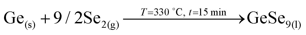
CZGeSe absorber layers were synthesized through a sequential deposition of metallic precursors on Mo-coated soda lime glass substrates. The stack order used in this experiment was Cu/Zn/Ge, deposited by DC magnetron sputtering (Alliance AC450). Cu-poor and Zn-rich composition was confirmed by X-ray fluorescence (XRF, Fischerscope XVD) being the cationic ratios: Cu/(Zn + Ge) = 0.65 and Zn/Ge = 1.06. The as deposited precursors were placed into a graphite box with an additional amount of germanium and selenium (100 mg of Se and 5 mg of GeSe2) to provide Ge + Se atmosphere during the thermal treatment. The annealing process was performed in a conventional tubular furnace following a two-step profile process, the first one at 330 °C for 30 min with a heating rate of 20 °C min−1 at 1.5 mbar Ar pressure, and the second step at 480 °C for a dwelling time of 15 min at 1 bar Ar pressure. The cooling down process occurred naturally, taking typically 1 hour. In order to study the formation pathways for this system, a special break-off experiment was implemented, where the annealing process was stopped at different times during the synthesis and crystallization stages. To ensure reproducibility and minimize experimental errors, this experiment was performed repeatedly on two samples simultaneously in each process, and the graphite boxes were cleaned thoroughly prior to each annealing step. Fig. 1 shows the thermal annealing profile used in this work, where the different stages and the selected conditions to stop the thermal routine are highlighted. The samples obtained from T1 to T6 were fully characterized. | ||
| Fig. 1 Thermal profile used in this work including the two specific steps, one for the synthesis of the material at 330 °C, and one for the crystallization at 480 °C, and the intermediate points where the annealing process was stopped at (points T1 to T6). | ||
Solar cell fabrication
Solar cells were completed with the growth of the CdS buffer layer on the absorber by chemical bath deposition (CBD),35 immediately after a KCN etching (2% w/v, room temperature, 2 min). Then, the i-ZnO (50 nm) + ITO (In2O3:SnO2, 250 nm) window layer was deposited by DC-pulsed sputtering. Finally, 3 × 3 mm2 individual solar cells were defined by means of a microdiamond scriber MR200 OEG. Neither anti-reflective coating nor metallic grids were used in the devices presented in this work.Films and devices characterization
J–V curves were measured using a 1 sun calibrated 3000 class AAA solar simulator (Abet Technologies, AM 1.5G illumination). The measurements were carried out at room temperature after calibrating the solar simulator using a c-Si reference cell. Spectral response/external quantum efficiency (EQE) measurements were performed using a Bentham PVE300 system (Bentham Instruments Ltd, Berkshire, UK) calibrated with c-Si and Ge photodiodes. SEM images were obtained with a ZEISS Series Auriga microscope using 5 kV accelerating voltage. Raman analysis were carried out using a Horiba Jobin Yvon LabRam HR800-UV coupled with an Olympus metallographic microscope. Three excitation wavelengths were used: 442 nm, 532 nm and 785 nm. X-ray diffraction patterns were collected with a Bruker D8-diffractometer in Bragg–Brentano geometry, using a Monochromatized CuK-L3 X-ray source (1.540598 Å) and a LynxEye PSD detector.Results and discussion
First of all, a complete characterization of the morphology and composition of the samples T1 to T6 obtained from the break-off experiment was performed. Fig. 2 shows the cross-sectional SEM images, together with the estimated thicknesses and Se concentration measured by XRF for all these samples. In sample T1 (330 °C, 1 min), an unexpected large amount of Se is obtained, (almost 50 at%) being nearly the expected stoichiometric value. This strongly differs from the Sn-pure compound where normally, even at higher temperatures, only a fraction of the required Se is incorporated at the very beginning of the synthesis step.9 Additionally, this is a clear indication that there is a very different incorporation mechanism for Se in CZGeSe when compared with CZTSe, being somehow accelerated in the first case. In fact, and as can be seen in the cross-sectional SEM images at the top of Fig. 2, the morphology is surprisingly smooth at the surface, and very small dendritic growths start to be observed in the back region, close to the Mo contact. This type of very flat surface morphology is only possible if some liquid phase is formed at the very beginning of the synthesis process. This, once again, differs from the CZTSe and other kesterite compounds where rough and nanocrystalline structures are usually observed at this early stage of the synthesis process.9,33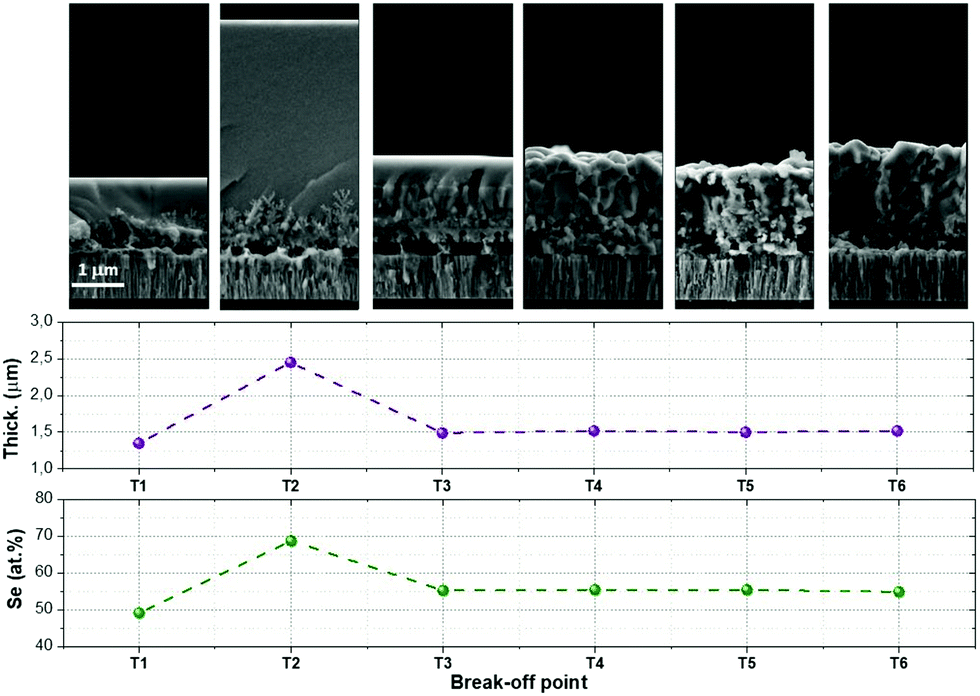 | ||
| Fig. 2 Cross-sectional SEM images and XRF results obtained for the samples T1 to T6 (layer thickness and Se content). | ||
This effect is even magnified for the sample obtained in the break-off point T2. As can be clearly seen in the SEM image at the top part of Fig. 2, the thickness increases up to 2–3 times, the surface becomes even flatter, the dendrites at the back are better distinguishable, and the XRF analysis indicates that the sample becomes extremely Se-rich (up to 70 at% of Se). This result can only be explained by the presence of a Se-rich liquid phase, as has been previously suggested for samples containing small Ge amounts.9,12 In the case of the Ge-pure compound, the liquid phase is the dominant one during a relevant part of the synthesis process. To better understand the nature of the liquid phase, Fig. 3a shows a schematic representation of the Ge–Se phase diagram in the Se-rich region.36
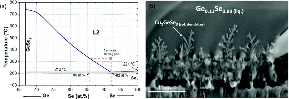 | ||
| Fig. 3 Schematic representation of the Ge–Se phase diagram in the Se-rich region (a). Detail of the dendrites formed at the back region corresponding to the break-off point T2. | ||
As can be seen, a eutectic point is formed in the highly Se-rich zone, with a composition of approximately Ge0.08Se0.92 and a melting point of 212 °C, well below to the stablished temperature for the synthesis stage (330 °C). This special regime can have two very important consequences on the synthesis step, namely:
1. Synthesis assisted by a superheated liquid:
Considering that the temperature during the synthesis process is 330 °C, this implies that the Ge-Se liquid phase is superheated (the melting point is 212 °C). It is well known from the metallurgical field that fast cooled superheated/supersaturated liquids lead easily to the formation of dendritic growth,37 as the ones observed also in Fig. 3b. This is another conclusive evidence of the formation of a liquid phase in the system. In Fig. 3a the cooling down process of the superheated liquid is also schematized, showing that a solid phase with composition between Ge0.14Se0.86 and Ge0.08Se0.92 is obtained, in good agreement with the XRF measurement which gives a phase with an average composition of Ge0.11Se0.89.
2. Extended solid–liquid–vapor (SLV) type growth:
The presence of a liquid phase in the system suggests that an extended SLV-like type growth is occurring for the synthesis of CZGeSe. In a first stage (break-off points T1 and T2), selenium gas from the atmosphere is absorbed in the precursor forming the eutectic Se-rich Ge–Se phase which melts at temperatures well below 330 °C. Following this, the eutectic compounds start to decompose and the solid phase dissolved in the liquid precipitates, while Se2(g) is released and the liquid phase is consumed, as can be seen in the SEM cross-section and the XRF measurements from break-off points T2 to T3. This shows that the SLV growth is not only useful for the growth of nano-sized structures, but also for the effective crystallization of thin films in an extended version of this process.
The combined XRD and Raman phase analysis that will be presented later will give additional insights about the compounds formed in these intermediate points of the CZGeSe synthesis, to demonstrate the peculiarities of this particular kesterite system.
Following with Fig. 2, at the break-off point T3, most of the Ge–Se liquid phase was released and the layer recovered the expected thickness and Se content. Note that the layer is slightly delaminated from the substrate; this is probably due to a combination of factors including de-wetting problems of the Ge–Se liquid phase and the Glass/Mo substrate, as well as relatively fast Cu out-diffusion as will be shown later. The surface of the film is still flat enough to indicate that the liquid phase is present in the system, but the dendritic growth is not observed anymore; instead, a nanocrystalline layer appears suggesting that a new crystalline phase has been completely formed. Finally, once the temperature is increased in the second stage (crystallization stage, from break-off points T4 to T6), the evidences of a liquid phase presence disappear, and the thin film becomes more and more crystalline. Following this logic, we can infer that the synthesis process finishes during the T1–T3 stage, and that the T4–T6 is a pure crystallization step.
To extend the analysis to the cations present in the system, Fig. 4 shows the evolution of the Se/Ge ratio and the different cationic ratios through the complete T1–T6 process. As expected, and in good agreement with Fig. 2 and 3, the Se/Ge ratio strongly increases for the break-off point T2 and then decreases to stabilize during the crystallization process. This behavior is markedly different to what is commonly observed in the pure-Sn compound, therefore we can consider that Ge acts like a catalyst, capturing Se from the atmosphere through the formation of the eutectic Ge–Se compound (hereinafter called GeSe9 for simplification) and drastically changing the characteristics of the synthesis process. Concerning the cations composition relationships, Cu/Zn ratio is quite stable during the whole process suggesting that these elements only experience diffusion processes during the annealing and, as expected, are not exchanged with the atmosphere. Nevertheless, Cu/Ge and Zn/Ge ratios increase after the break-off point T3, suggesting that mainly at the end of the synthesis processes, and beginning of the crystallization, some Ge is exchanged with the atmosphere, most probably due to the decomposition and evaporation of the eutectic GeSe9 liquid phase.
 | ||
| Fig. 4 Different compositional ratios obtained during the T1–T6 process measured by XRF. | ||
Complementary information can be obtained from SEM/EDX combined surface analysis. Fig. 5 shows the SEM top view of samples T1, T2, T3 and T4, and the corresponding EDX mapping, where Cu, Zn, Ge and Se intensity maps are shown. For T1 a smooth surface with a homogeneous distribution of all the elements is observed, suggesting that at early stages of the Ge–Se liquid phase formation there is not yet enough energy in the system to provoke large diffusion of the different elements. The surface morphology drastically changes for T2, where large (200–500 μm) “wave-like” structures are observed, corroborating the presence of a liquid phase. The formation of these morphologies suggests that the Ge–Se liquid phase does not wet completely the metallic surface below. In addition, in the frontiers of these “wave-like” structures, Cu, Zn and Ge can clearly be seen, while they are completely depleted of Se. It is also confirmed that these “wave-like” structures are only composed of Ge and Se. At T3, these structures cover less surface area, being flatter and more extended, consisting of the remnant Ge–Se liquid phase not evaporated yet. Below them, Cu, Zn, Ge and Se are clearly detected suggesting that most probably, the formation of CZGeSe is already occurring at this stage, or at least more complex selenide binary or ternary compounds are formed. Finally, by just increasing the temperature from T3 to T4, first crystalline structures start to be observed at the surface, and the elemental distribution becomes more homogenous, suggesting that all the Ge–Se liquid phase has been released from the system. Note that in some specific areas, an increased Zn concentration is detected, most probably related to the formation of an excess of ZnSe, due to the Zn-rich composition of the precursor that is also commonly observed in the pure-Sn compound.38
 | ||
| Fig. 5 Top view SEM images and corresponding Cu, Zn, Ge and Se compositional mappings obtained by EDX, for samples T1, T2, T3 and T4. The red squares in the left images delimitate the area where the EDX mappings were acquired. | ||
As a summary of this first morphology/composition characterization, the pure Ge kesterite formation seems to proceed very differently than the pure Sn one.9,12 Interestingly, Ge acts like a “catalyst” in the system, trapping Se from the atmosphere and forming a superheated liquid phase with approximately 10% of Ge and 90% of Se, which promotes a S–L–G type growth for the formation of CZGeSe. Now, it becomes very relevant to understand which phases are present at the different stages and their role during the kesterite formation.
For this purpose, in-depth compositional analysis, using Auger spectroscopy, and detailed phase analysis, using XRD and multi-wavelength Raman spectroscopy, were combined. Fig. 6 shows the in-depth Auger profile for Cu, Zn, Ge and Se (Mo is shown in grey scale as reference to identify the surface and back region), in a colored schema for a better visualization of their inter-diffusion (raw profiles are presented in Fig. S1 of the ESI†). In Fig. 6, each element intensity was normalized to the highest value. In the following, these in-depth composition profiles will be analyzed together with the XRD and Raman spectroscopy characterization presented in Fig. 7 (with 442 nm excitation wavelength, while spectra obtained with 785 nm and 532 nm excitation wavelengths are reported in Fig. S2 of the ESI†).
 | ||
| Fig. 6 In-depth Auger spectroscopy compositional profiles, showing the distribution of Cu, Zn, Ge and Se, from T1 to T6. The individual signals were normalized to the highest intensity value. | ||
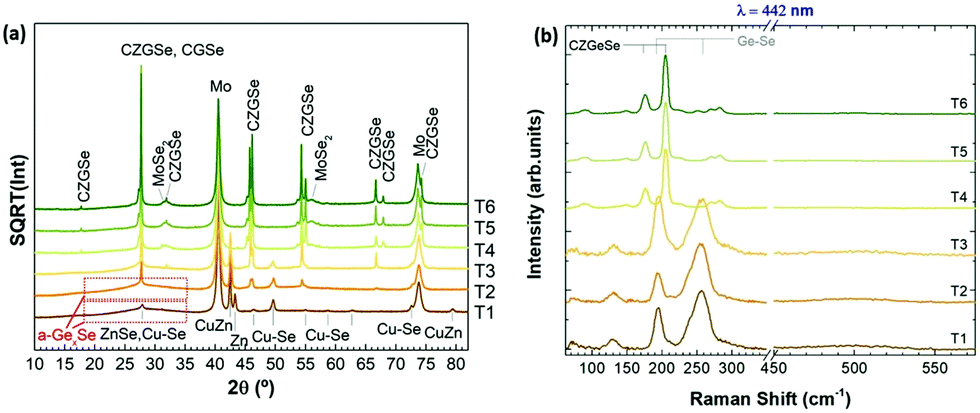 | ||
| Fig. 7 XRD diffractograms (a), and surface Raman spectra with 442 nm excitation wavelength (b), of samples T1 to T6. | ||
Comparing then Fig. 6 and 7, the following information can be drawn in terms of elemental distribution and phase formation and reaction during the whole reactive annealing process:
T1
Auger spectroscopy suggests that most of the Se is combined with Ge at the surface of the layer, corroborated by XRD and Raman spectroscopy, and confirming that the liquid phase is formed by these two elements. This implies that Se is in-diffusing from the atmosphere being very efficiently captured by the Ge top layer. On the other hand, the Cu and Zn signals are almost overlapping, and considering that the Zn signal extends up to the back contact, we can infer that Cu starts to out-diffuse. A slight overlap between Cu/Zn and Se in-depth distribution is observed suggesting that some chalcogenides of these elements are most probably being formed although in tiny quantities; and in fact XRD indicates the possible presence of Cu–Se and maybe ZnSe. Nevertheless, it is clear that at this stage large quantities of metallic phases are still present (mainly Cu–Zn and most probably as Cu5Zn8 brass phase).32Confirmed phases: Ge–Se (∼10 at% Ge–90 at% Se), Cu–Zn brasses, metallic Zn, Cu–Se, ZnSe?
Considering this, the main characteristics of the T0–T1 step are:
• Fast Se in-diffusion and incorporation from the atmosphere through the formation of the GeSe9 liquid phase.
• Ge acts as a “catalyst” to trap Se from the atmosphere.
• Cu starts out-diffusing from the back region towards the surface.
The main reactions occurring can be summarized as follow:

(Partial, not completed).

T2
The elemental distribution slightly changes showing a clear overlap between the Ge and Se signals, confirming the maximization of this phase in agreement with SEM, XRF, Raman and XRD. Interestingly, a first split of the Cu signal is observed, where some Cu starts to rapidly diffuse towards the surface, then it is depleted in the middle where the Zn concentration is maximized, and again increases towards the back region. There is almost no overlap between the Ge and Zn signals, confirming the phase separation of these two elements and suggesting that kesterite is not formed yet, or in very small quantities. Apparently, while Cu–Se is soluble in the Ge–Se liquid phase, ZnSe is fully insoluble, delaying the formation of kesterite. Raman spectroscopy confirms again the formation of large amounts of Ge–Se (Se-rich) phase. Complementary, XRD confirms the presence of Cu–Zn brasses and Cu–Se, and the absence of metallic Zn. A strong diffraction peak is developed at 27.5°, together with other peaks at about 46° and 55°, which in principle can either be assigned to tetragonal CZGeSe, orthorhombic Cu2GeSe3 and/or cubic ZnSe. Nevertheless, considering the in-depth Auger distribution of elements, the formation of CZGeSe is barely expected, and for ZnSe most probably only few quantities are formed, suggesting that the formation of Cu2GeSe3 ternary compound is the most plausible explanation in form of dendrites developed at the interface of the GeSe9 liquid phase and the metallic back region, as suggested in Fig. 3. This is further supported by specific Raman measurements that were performed in polished samples in order to have access to in-depth structural information, as shown in Fig. S3 and S4 of the ESI.† These figures strongly support the formation of a Cu2GeSe3 ternary phase just below the GeSe9 liquid phase.Confirmed phases: Ge–Se (∼10 at% Ge–90 at% Se), Cu–Zn brasses, Cu–Se, Cu2GeSe3, ZnSe?
The main characteristics of the T1–T2 step are:
• Even faster Se in-diffusion and incorporation from the atmosphere towards the layers through the formation of large amounts of GeSe9 liquid phase.
• Increased Cu out-diffusion, splitting its distribution in two regions, the back region where the Cu–Zn alloy is unreacted, and the middle region where Cu diffuses by reaction with GeSe9.
The main reactions occurring during this step can be summarized as follows:

(Almost completed, large amounts of the liquid phase are observed)
(First direct evidences of the formation of Cu2GeSe3 ternary phase, by reaction of CuSe with GeSe9 liquid phase, with the release of Se2 gas).

T3
At the end of the low temperature step (330 °C, 30 min), the previously described elemental distribution evolves towards a clearer phase separation. As it is observed in the corresponding Auger profile, Cu keeps diffusing towards the front region, together with Ge and Se. Then in the middle, Zn is clearly overlapping with Se suggesting that it is at least partially selenized, and finally the remaining Cu is accumulated at the back and slightly selenized or unreacted yet. This confirms the split of Cu into two zones, the upmost that is fully soluble into the Ge–Se liquid phase, and the lowermost that is formed by ZnSe, Cu–Se and Cu–Zn phases, in this order. Raman confirms still the presence of GeSe9 (Se-rich) liquid phase, while XRD and Raman prove the presence of Cu2GeSe3, Cu–Se and Cu–Zn alloys. Confirmed phases: Ge–Se (∼10 at% Ge–90 at% Se), Cu–Zn brasses, Cu–Se, Cu2GeSe3, ZnSe.The main characteristics of the T2–T3 step are:
• A clear Se out-diffusion (and release as Se2(g)) due to the reaction between the Ge–Se liquid phase and CuSe to form the ternary compound.
• Full splitting of the Cu content in two regions, the one containing the ternary compound and the one with still unreacted Cu–Zn alloys and CuSe.
The main reactions occurring during this last part of the low temperature dwell time can be summarized as follow:

(The formation of Cu2GeSe3 ternary phase is accelerated, with strong release of Se2 gas).

T4–T6
Once the temperature is increased up to 480 °C (crystallization temperature), the in-depth compositional profile changes drastically, and a more uniform distribution of the different elements is clearly observed, indicating that CZGeSe is rapidly formed during the ramping time (the system needs approximately 7.5 min to go from 330 °C up to 480 °C). Surface Raman spectroscopy as well as XRD confirm the presence of good crystalline quality CZGeSe phase from the very beginning of the crystallization step, although some secondary phases still remain in the system depending on the time. At T4, some Cu and Zn are still accumulated at the back, but in principle fully selenized. In fact, only the presence of ZnSe is suggested by XRD by the existence of a shoulder at 27.3°. At T5, most of the Cu is clearly homogenized through the whole thickness being most probably fully incorporated into the kesterite phase. Some ZnSe is detected towards the back region. At T6, well crystallized CZGeSe is still the main phase, although probably ZnSe has started to diffuse towards the front. In all this process, the FWHM and the position of the main Raman peak of CZGeSe are unchanged (being 8.5 cm−1 and 163 cm−1 respectively).Confirmed phases: Cu2ZnGeSe4, ZnSe.
The main characteristics of the T3–T6 step are:
• Fast diffusion of all the elements, and homogeneous in-depth distribution.
• All the reactions are finished in the short T3–T4 step (ramping from low to high temperature), and T4–T6 step is mainly for the crystallization of the absorber and probably re-distribution of remaining secondary phases (mainly or exclusively ZnSe).
The main reactions occurring during this annealing time can be summarized as follow:

(Completed in the T3–T4 step)

(Reaction most probably initiated immediately after T3 and completed at T4 in very short time).

All this demonstrates the peculiarities of the formation of CZGeSe, with a mechanism that involves vapor, liquid and solid phases. To summarize this, Fig. 8 shows the proposed schema illustrating the formation pathways of CZGeSe, where the key steps are highlighted. In fact, the system evolves during the annealing process from simple elemental species towards more complex binary compounds first, then ternary, and finally the quaternary kesterite. Basically and based on the schematic representations of Fig. 8, to form the CZGeSe kesterite by this sequential process, it is needed:
 | ||
| Fig. 8 Proposed schema of the formation pathways of CZGeSe. | ||
1. In-diffusion of Se to form the binary GeSe9 liquid phase that is not only an intermediate specie to form kesterite, but also act as a catalyst.
2. Partial selenization of brasses into binary CuSe(s) and ZnSe(s) that promotes the out-diffusion of Cu (either as metal or most probably as CuSe).
3. Reaction of CuSe(s) with GeSe9(l) to form the ternary Cu2GeSe3(s) with the release of Se2(g).
4. Reaction of Cu2GeSe3(s) and ZnSe(s) to form quaternary Cu2ZnGeSe4(s).
This makes not only unique the synthesis route of this material among all the kesterite family, but also contributes to clearly identify the most relevant and challenging aspects for future improvements. In particular, as very positive aspects we can mention the presence of a GeSe9(l) phase that catalyzes the Se incorporation and drives the formation reaction. The apparent non-solubility of ZnSe into the GeSe9(l) phase and the relatively fast out-diffusion of Cu (probably as CuSe) lead to the formation of the Cu2GeSe3(s) ternary phase as the final intermediate compound for the formation of kesterite. All this synergy between a system that evolves smoothly from more simple up to more complex species involving liquid, solid and vapor phases, enhances the probability of completing all the reactions minimizing the risk of presence of unreacted secondary phases at the end of the synthesis process. In fact, the only secondary phase probably present is ZnSe.
Conversely, among the challenging characteristics of the synthesis of this material, the formation of large amounts of GeSe9(l) liquid phase can be also problematic. Back in Fig. 5, it was shown that the liquid phase seems to not completely wet the surface, forming non-homogenous “wave-like” structures that could introduce non-homogeneities in the final absorber, or even contribute to a partial peel-off from the substrate. Additionally, the relatively fast Cu-out diffusion observed during the first stage of the synthesis can also contribute to the formation of voids at the back contact, as has been demonstrated in other related technologies.9,32,39
Finally, to support the relevance of this study, solar cells were prepared with absorbers synthesized with the presented thermal routine, which was optimized prior to the experiments presented in this work. Fig. 9 (left) shows the illuminated J–V curve (AM1.5) of one of the champion cells, demonstrating a 6.5% efficiency device with 556 mV of VOC as it is also summarized in Table 1 (neither anti-reflection coating nor metallic grid were used in these devices). This is one of the highest efficiencies reported so far for the pure Ge compound, with a VOC and a FF almost equal to the current record.20 The external quantum efficiency (EQE) spectrum shows a maximum of roughly 75%, but with a flat aspect between 500–700 nm, which may suggest a relatively good quality CZGeSe/CdS junction and CZGeSe bulk material. From 700 nm, the EQE starts to decrease, most probably due to recombination problems at the back contact that could be related to the presence of voids in this region. The improvement of the de-wetting problems as well as the fast Cu out-diffusion are two specific issues that could contribute to boost, at least partially, the conversion efficiency of this material in the future.
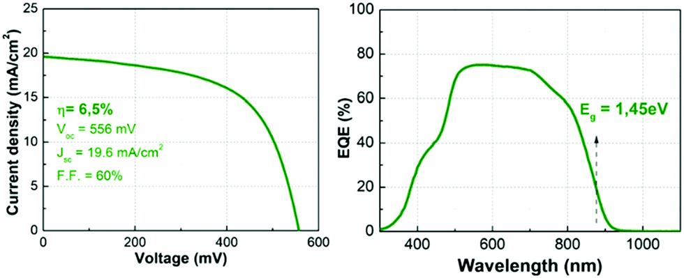 | ||
| Fig. 9 Illuminated J–V curve (AM1.5) with the corresponding optoelectronic parameters (left side), and external quantum efficiency (EQE) spectrum with the estimated bandgap (right side). | ||
Conclusions
The detailed reaction mechanisms for the formation of CZGeSe by a sequential process (sputtering of metallic stacks followed by reactive annealing) was investigated by the implementation of a break-off annealing experiment, and with the combination of detailed compositional, morphological and structural characterization. Unique properties are observed in this system, where a eutectic GeSe9 liquid phase is rapidly formed at the surface, governing all the subsequent reactions through an extended solid–liquid–vapor reaction. Conforming the synthesis steps proceed, CuSe and ZnSe are formed by the direct selenization of the brass alloy. Then, part of this CuSe starts to out-diffuse and dissolve in the GeSe9 superheated liquid phase, while the ZnSe is apparently non soluble. Subsequently, CuSe and GeSe9 react forming the ternary Cu2GeSe3 compound, which reacts with the ZnSe very quickly when the temperature is increased up to 480 °C, forming finally the Cu2ZnGeSe4 kesterite. The unexpected formation of the GeSe9 liquid phase confers to the system special properties, helping to drive the formation reaction and minimizing the presence of possible secondary phases. By optimizing this approach, solar cell devices with conversion efficiency at the level of the highest reported in the literature are presented, identifying de-wetting issues related to the GeSe9 phase, and fast Cu-out diffusion as two relevant issues to be improved in order to boost the performance of this technology.Conflicts of interest
There are no conflicts to declare.Acknowledgements
This research was supported by the H2020 Programme under the project INFINITE-CELL (H2020-MSCA-RISE-2017-777968), by the Spanish Ministry of Science, Innovation and Universities under the IGNITE project (ENE2017-87671-C3-1-R), and by the European Regional Development Funds (ERDF, FEDER Programa Competitivitat de Catalunya 2007–2013), and by the Moroccan Ministry of Higher Education and Research under the project PPR/2015/59. Authors from IREC and the University of Barcelona belong to the SEMS (Solar Energy Materials and Systems) Consolidated Research Group of the “Generalitat de Catalunya” (Ref. 2017 SGR 862).References
- S. Giraldo, Z. Jehl, M. Placidi, V. Izquierdo-Roca, A. Pérez-Rodríguez and E. Saucedo, Adv. Mater., 2019, 1806692 CrossRef PubMed.
- W. Wang, M. T. Winkler, O. Gunawan, T. Gokmen, T. K. Todorov, Y. Zhu and D. B. Mitzi, Adv. Energy Mater., 2014, 4, 1301465 CrossRef.
- L. H. Wong, A. Zakutayev, J. D. Major, X. Hao, A. Walsh, T. K. Todorov and E. Saucedo, J. Phys. Energy, 2019, 1, 032001 CrossRef.
- P. Jackson, R. Wuerz, D. Hariskos, E. Lotter, W. Witte and M. Powalla, Phys. Status Solidi RRL, 2016, 10, 583–586 CrossRef CAS.
- M. A. Green, E. D. Dunlop, D. H. Levi, J. Hohl-Ebinger, M. Yoshita and A. W. Y. Ho-Baillie, Prog. Photovoltaics, 2019, 27, 565–575 Search PubMed.
- M. Dimitrievska, A. Fairbrother, E. Saucedo, A. Pérez-Rodríguez and V. Izquierdo-Roca, Sol. Energy Mater. Sol. Cells, 2016, 149, 304–309 CrossRef CAS.
- S. Rühle, Sol. Energy, 2016, 130, 139–147 CrossRef.
- M. Neuschitzer, J. Marquez, S. Giraldo, M. Dimitrievska, M. Placidi, I. Forbes, V. Izquierdo-Roca, A. Pérez-Rodriguez and E. Saucedo, J. Phys. Chem. C, 2016, 120, 9661–9670 CrossRef CAS.
- S. Giraldo, E. Saucedo, M. Neuschitzer, F. Oliva, M. Placidi, X. Alcobé, V. Izquierdo-Roca, S. Kim, H. Tampo, H. Shibata, A. Pérez-Rodríguez, P. Pistor, A. Perez-Rodriguez and P. Pistor, Energy Environ. Sci., 2018, 11, 582–593 RSC.
- K. Biswas, S. Lany and A. Zunger, Appl. Phys. Lett., 2010, 96, 2012–2015 Search PubMed.
- S. Bag, O. Gunawan, T. Gokmen, Y. Zhu and D. B. Mitzi, Chem. Mater., 2012, 24, 4588–4593 CrossRef CAS.
- S. Giraldo, M. Neuschitzer, T. Thersleff, S. Lõpez-Marino, Y. Sánchez, H. Xie, M. Colina, M. Placidi, P. Pistor, V. Izquierdo-Roca, K. Leifer, A. Pérez-Rodríguez and E. Saucedo, Adv. Energy Mater., 2015, 5, 1501070 CrossRef.
- S. Giraldo, M. Neuschitzer, M. Placidi, P. Pistor, A. Perez-Rodriguez and E. Saucedo, IEEE J. Photovoltaics, 2016, 6, 754–759 Search PubMed.
- S. Kim, K. M. Kim, H. Tampo, H. Shibata and S. Niki, Appl. Phys. Express, 2016, 9, 1–5 Search PubMed.
- C. J. Hages, S. Levcenco, C. K. Miskin, J. H. Alsmeier, D. Abou-Ras, R. G. Wilks, M. Bär, T. Unold and R. Agrawal, Prog. Photovoltaics, 2015, 23, 376–384 CAS.
- M. Neuschitzer, E.-R. Moises, M. Guc, J. Prieto, S. Giraldo, I. Forbes, P.-R. Alejandro and E. Saucedo, J. Mater. Chem., 2018, 6, 11759–11772 RSC.
- J. Márquez, H. Stange, C. J. Hages, N. Schaefer, S. Levcenko, S. Giraldo, E. Saucedo, K. Schwarzburg, D. Abou-Ras, A. Redinger, M. Klaus, C. Genzel, T. Unold and R. Mainz, Chem. Mater., 2017, 29, 9399–9406 CrossRef.
- A. D. Collord and H. W. Hillhouse, Chem. Mater., 2016, 28, 2067–2073 CrossRef CAS.
- S. Kim, K. M. Kim, H. Tampo, H. Shibata, K. Matsubara and S. Niki, Sol. Energy Mater. Sol. Cells, 2016, 144, 488–492 CrossRef CAS.
- L. Choubrac, G. Brammertz, N. Barreau, L. Arzel, S. Harel, M. Meuris and B. Vermang, Phys. Status Solidi, 2018, 215, 1800043 CrossRef.
- S. Sahayaraj, G. Brammertz, B. Vermang, T. Schnabel, E. Ahlswede, Z. Huang, S. Ranjbar, M. Meuris, J. Vleugels and J. Poortmans, Sol. Energy Mater. Sol. Cells, 2017, 171, 136–141 CrossRef CAS.
- T. Schnabel, M. Seboui and E. Ahlswede, RSC Adv., 2017, 7, 26–30 RSC.
- R. Gunder, J. A. Márquez Prieto, G. Gurieva, T. Unold and S. Schorr, CrystEngComm, 2018, 20, 1491–1498 RSC.
- S. Levcenko, R. Caballero, L. Dermenji, E. V. Telesh, I. A. Victorov, J. M. Merino, E. Arushanov, M. Leon and I. V. Bodnar, Opt. Mater., 2015, 40, 76–80 CrossRef CAS.
- G. Swapna Mary, G. Hema Chandra, M. Anantha Sunil and M. Gupta, J. Electron. Mater., 2018, 47, 800–810 CrossRef CAS.
- S. Niedenzu, G. Gurieva and S. Schorr, Thin Solid Films, 2019, 669, 625–628 CrossRef CAS.
- K. Nagaya, S. Fujimoto, H. Tampo, S. Kim, M. Nishiwaki, Y. Nishigaki, M. Kato, H. Shibata and H. Fujiwara, Appl. Phys. Lett., 2018, 113, 093901 CrossRef.
- G. Brammertz, T. Kohl, J. De Wild, M. Meuris, B. Vermang and J. Poortmans, Thin Solid Films, 2019, 670, 76–79 CrossRef CAS.
- K. Tsuji, T. Maeda and T. Wada, Japanese Journal of Applied Physics, Japan Society of Applied Physics, 2018, vol. 57 Search PubMed.
- M. Grossberg, K. Timmo, T. Raadik, E. Kärber, V. Mikli and J. Krustok, Thin Solid Films, 2015, 582, 176–179 CrossRef CAS.
- M. Courel, T. G. Sanchez, N. R. Mathews and X. Mathew, J. Phys. D: Appl. Phys., 2018, 51, 095107 CrossRef.
- A. Fairbrother, X. Fontané, V. Izquierdo-Roca, M. Espíndola-Rodríguez, S. López-Marino, M. Placidi, L. Calvo-Barrio, A. Pérez-Rodríguez and E. Saucedo, Sol. Energy Mater. Sol. Cells, 2013, 112, 97–105 CrossRef CAS.
- A. Hernández-Martínez, M. Placidi, L. Arqués, S. Giraldo, Y. Sánchez, V. Izquierdo-Roca, P. Pistor, M. Valentini, C. Malerba and E. Saucedo, ACS Appl. Energy Mater., 2018, 1, 1981–1989 CrossRef.
- W. C. Hsu, I. Repins, C. Beall, C. Dehart, B. To, W. Yang, Y. Yang and R. Noufi, Prog. Photovoltaics, 2014, 22, 35–43 CAS.
- M. Neuschitzer, Y. Sanchez, S. Lõpez-Marino, H. Xie, A. Fairbrother, M. Placidi, S. Haass, V. Izquierdo-Roca, A. Perez-Rodriguez and E. Saucedo, Prog. Photovoltaics, 2015, 23, 1660–1667 CAS.
- H. Ipser, M. Gambino and W. Schuster, Monatsh. Chem., 1982, 113, 389–398 CrossRef CAS.
- C. Wang, J. Zhang, M. Zou, L. Liu and H. Fu, Jinshu Xuebao, 2010, 46, 674–680 CAS.
- S. Lõpez-Marino, Y. Sánchez, M. Placidi, A. Fairbrother, M. Espindola-Rodríguez, X. Fontané, V. Izquierdo-Roca, J. Lõpez-García, L. Calvo-Barrio, A. Pérez-Rodríguez and E. Saucedo, Chem. – Eur. J., 2013, 19, 14814–14822 CrossRef PubMed.
- E. Avancini, D. Keller, R. Carron, Y. Arroyo-Rojas Dasilva, R. Erni, A. Priebe, S. Di Napoli, M. Carrisi, G. Sozzi, R. Menozzi, F. Fu, S. Buecheler and A. N. Tiwari, Sci. Technol. Adv. Mater., 2018, 19, 871–882 CrossRef CAS PubMed.
Footnote |
| † Electronic supplementary information (ESI) available. See DOI: 10.1039/c9tc06728k |
| This journal is © The Royal Society of Chemistry 2020 |