
 Open Access Article
 This Open Access Article is licensed under a Creative Commons Attribution-Non Commercial 3.0 Unported Licence
Utilizing Diels–Alder “click” chemistry to functionalize the organic–organic interface of semiconducting polymers†
David
Burmeister
 a,
Lukas
Ahrens
bc,
Andreas
Opitz
d,
Giovanni
Ligorio
a,
Felix
Hermerschmidt
a,
Daniel
Jänsch
bc,
Jan
Freudenberg
*bc,
Uwe H. F.
Bunz
b,
Klaus
Müllen
e and
Emil J. W.
List-Kratochvil
*af
a,
Lukas
Ahrens
bc,
Andreas
Opitz
d,
Giovanni
Ligorio
a,
Felix
Hermerschmidt
a,
Daniel
Jänsch
bc,
Jan
Freudenberg
*bc,
Uwe H. F.
Bunz
b,
Klaus
Müllen
e and
Emil J. W.
List-Kratochvil
*af
aInstitut für Chemie, Institut für Physik, IRIS Adlershof, Humboldt- Universität zu Berlin, Brook-Taylor-Str. 6, 12489 Berlin, Germany. E-mail: emil.list-kratochvil@hu-berlin.de
bOrganisch-Chemisches Institut, Universität Heidelberg, Im Neuenheimer Feld 270, 69120 Heidelberg, Germany. E-mail: freudenberg@oci.uni-heidelberg.de
cInnovationLab, Speyerer Str. 4, 69115 Heidelberg, Germany
dInstitut für Physik, IRIS Adlershof, Humboldt-Universität zu Berlin, Brook-Taylor-Str. 6, 12489 Berlin, Germany
eMax Planck Institute for Polymer Research, Ackermannweg 10, Mainz D-55128, Germany
fHelmholtz-Zentrum für Materialien und Energie GmbH, Brook-Taylor-Straße 6, 12489 Berlin, Germany
First published on 27th January 2020
Abstract
Tuning the energy levels of organic semiconductors in a predictable and durable manner is a challenging, yet necessary task to obtain high performance electronic and optoelectronic devices. Thermal diffusion and drift of dopants used for energy level control in the mostly van der Waals-cohered solids results in the degradation of the defined interfaces that all electronic and optoelectronic devices rely on. An important goal is therefore their spatial fixation in multilayer organic device stacks. This work aims at covalently functionalizing the interface of an immobilized organic semiconductor polymer. To achieve this goal, the side chains of a polyfluorene are equipped with biscyclopentadienyl moieties which undergo thermal fragmentation via retro-Diels–Alder reactions to yield cyclopentadienyl functions. Diels–Alder cycloadditions of these functional groups cross-link adjacent polymer chains. In a second step, unreacted cyclopentadienyl units at the interface are covalently functionalized with strong dienophiles through a Diels–Alder reaction from solution. This reaction sequence modifies the energetics and the work function at the interface. Transfer of our protocol to other conjugated polymers and/or reaction types paves the way to tunable energy levels at organic–organic interfaces and to universal introduction of functions at organic semiconductor interfaces after deposition from solution.
Introduction
Precisely controlling the electrical bulk and interface properties of inorganic element and compound semiconductors by impurity doping is a well-established concept and the foundation for today's semiconductor industry.1 Along the same lines, the functionalization of organic semiconductors (OSCs) with organic dopants has been the subject of research for the past thirty years. Homogeneously distributed dopants inside the semiconductors allow charge transfer and increase of charge carrier density in the semiconductor. This is used to tailor the charge transport properties and the energy level alignment to electrodes or other semiconductor layers.2Combining the best of two worlds (organic and inorganic semiconductors) has driven the exploration of “hybrid” interfaces. It allows tuning of the energy levels and work-functions at such hybrid interfaces using self-assembled monolayers (SAMs) and organic dopant molecules.3–5 However, in most cases, this approach still relies on a metal or inorganic semiconductor surface as the anchoring ground to spatially fix the SAM or dopant.6,7 Facing these limits, the full potential of organic electronics cannot be fully exploited.8–12 Charge transport and interface effects present in OSCs and at organic-organic junctions have been intensely investigated. This includes – besides the aforementioned bulk and interfacial doping – also blending of organic semiconductors with inert matrix molecules13 or aligning of molecules on top of aligned polymer films14 to improve ordering inside the OSC and to improve the charge carrier transport. However, spatially resolved and stable doping, or derivatization of solution-processable OSCs in particular remains challenging.4,15–17 Charge carrier injection and management, e.g. for recombination zones in organic light emitting diodes (OLEDs) or for charge extraction in (perovskite) solar cells, have to rely on multi-stack architectures. This so-called hetero-junction approach, in turn, depends on the energetic alignment of adjacent (organic) layers. Concepts are therefore needed to obtain OSCs with spatially defined, covalent, modular surface functionalizations to enhance conductivity, fill deep states or design recombination zones in OLEDs without contaminating the device stack.18–22
Handling high doping levels in organic devices is difficult since atomic dopants as well as bulky molecular dopants deposited by physical vapor deposition migrate in the device stack and tend to alter the sensitive interfaces or surrounding layers.23,24 Since small molecule OSCs, e.g. pentacene, as well as conjugated polymer OSCs, e.g. polyfluorenes, are mostly van der Waals-cohered solids, it is necessary to covalently bind dopant molecules to the OSC matrix.25 We recently demonstrated a way to avoid the diffusion and drift of dopant molecules in bulk by covalent anchoring to the OSC host-matrix.26 Still, modulating the work function (WF) of OSCs at the spatially defined organic–organic interface is hitherto unresolved.
In this contribution we demonstrate the first solution-based, selective, post-deposition covalent interface functionalization of a polymeric OSC. After spin-coating, polyfluorene PF (see Fig. 1a) is immobilized by thermal cross-linking and subsequently modularly functionalized at surface-bound, left-over reaction sites. Electron emission experiments are performed to characterize the covalent functionalization. X-ray photoelectron spectroscopy (XPS) is used to prove the physical presence of the functionalization by determining the elemental composition of the interface and in combination with an Ar+-ion sputtering to perform depth profiling. Ultraviolet photoelectron spectroscopy (UPS) allows one to monitor the effect of the functionalization on the energy levels. Undesirable degradation of the π-system of polyfluorene due to cross-linking or functionalization is monitored via absorption and photoluminescence emission experiments.
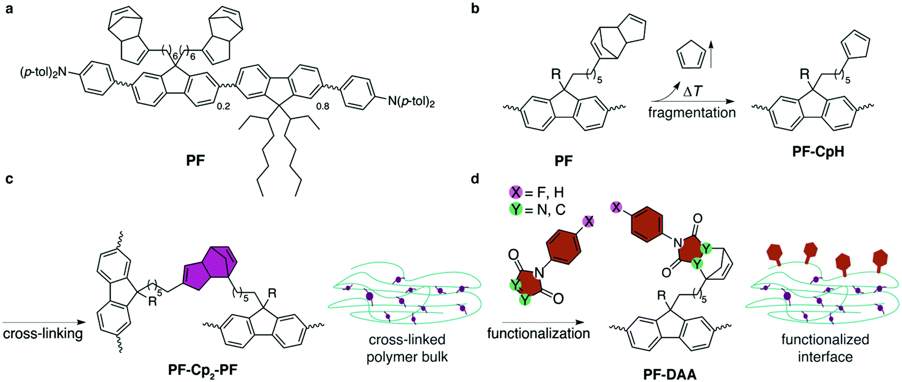 | ||
| Fig. 1 (a) Structural formula of polyfluorene derivative PF.27 (b) Fragmentation: spin-coated films are heated to 300 °C under inert atmosphere to cause fragmentation of the Cp2 moieties, liberating CpH units and generating reactive and cross-linkable cyclopentadienyl groups at the side-chains of PF-CpH. PF is substituted by the same two side-chains, the second of which is abbreviated by R, and can undergo the same reactions as sketched in (b–d). (c) Cross-linking: Diels–Alder-adduct formation of different polymer strands results in bis(cyclopentadien)ylene-bridged PF-Cp2-PF. (d) Hitherto unreacted cyclopentadienyl moieties are capped with dienophiles at the interface. | ||
Results and discussion
The conjugated polymer PF27 (Fig. 1a) is synthesized by statistic Yamamoto co-polymerization and carries N,N-di(p-tolyl)amino-phenyl end groups, to aid hole injection and transport, as well as ethylhexyl sidegroups to enhance solubility. About 20% of the fluorenylene units carry bis(cyclopentadien)yl groups.28 The solution-based immobilization/functionalization process is summarized in Fig. 1. Thermal fragmentation of PF by retro-Diels–Alder reaction in spin-coated films results in liberation of one molecule of volatile cyclopentadiene and generates one active cyclopentadienyl group per sidechain (Fig. 1b). The latter diene undergoes [4+2] Diels–Alder reaction with a second (or possibly a third) deprotected PF-CpH, cross-linking different polymer strands (Fig. 1c). If no Diels–Alder partner is available, which is most likely at the air–polymer-interface, PF-CpH reacts with a successively offered dienophile, such as maleimides or triazolinediones.Cross-linking of the films at 300 °C for 1 h in inert conditions resulted in solvent resistant films.27 The choice of temperature was based on thermogravimetric analysis (TGA) of the monomer.27 After cooling to room temperature, the cross-linked films were immersed in solutions of dienophiles (0.05 M, toluene) at 100 °C for two hours, to covalently functionalize the interface by formation of Diels–Alder adducts (PF-DAA) on the side chains (Fig. 1d). Four different dienophiles were tested regarding their use as covalent dienophile anchors: two highly reactive 4-phenyl-1,2,4-triazoline-3,5-diones (PTADs) and two N-phenylmaleimides (PMIs), both of which were either non-fluorinated (PTAD, PMI) or fluorinated at the para-position (4F-PTAD, 4F-PMI) of the phenyl ring. These molecules were chosen because of their systematic increase in electron affinity (EA) as a result of the increasing number of electronegative elements (nitrogen, fluorine). The higher the amount of electronegative atoms in the molecule within this series, the lower its energy of the lowest unoccupied orbital (LUMO) and, correspondingly, the higher its electron affinity (EAPMI < EA4F-PMI < EAPTAD < EA4F-PTAD).
Absorption (maximum at 3.2 eV) and emission (maximum at 2.9 eV) spectra remained essentially unaffected by cross-linking and subsequent functionalization (Fig. 2). Photoelectron spectra from UPS of a spin-coated thin film gave a WF value of 4.4 eV and a hole injection barrier (HIB) of 1.4 eV which is in agreement with results obtained for similar polymers.29 Investigation of the energy levels of immobilized films showed that the thermal cross-linking treatment resulted in a reversible change of the photoelectron spectrum (Fig. S1, ESI†), most likely reflecting water and oxygen inclusions leaving the sample during the annealing step. After exposure to ambient conditions, the initial equilibrium was regained, and the photoelectron spectrum of the non-cross-linked sample was almost completely restored after 1 h. Exposure to ambient conditions can be interpreted as weak p-doping (HIB changes from 1.7 eV (cross-linked) to 1.4 eV (cross-linked, 1 h ambient conditions)). To eliminate the influence of water and oxygen, sample preparation of functionalized films for UPS experiments were conducted in an inert atmosphere and transferred via a transfer arm from the glove box to the UPS analysis chamber.
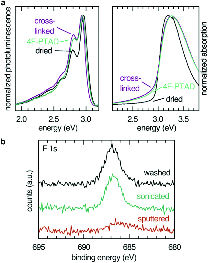 | ||
| Fig. 2 (a) Photoluminescence (left) and absorption (right) of PF films spin-coated and dried, cross-linked at 300 °C, and treated with 4F-PTAD. (b) XPS spectra of PF films functionalized with 4F-PTAD after washing with toluene (correction for sample charging, −7 eV), sonication for 30 min and removal of approximately 10 nm of the surface by Ar+ sputtering. The solvent resistant 4F-PTAD functionalized films show no reduction of fluorine F 1s signal after sonication in toluene for 30 min. Only after sputtering did the fluorine signal of the covalently attached dienophiles decrease. | ||
Modification of the film interfaces with dienophiles was first tested with the most potent dienophile, 4F-PTAD, which is approximately six orders of magnitude more reactive than the maleimides and considered a super-dienophile.30 The low-lying LUMO of the reactant is due to the nitrogen–nitrogen double bond and fluorination, the latter also acting as an atomic probe in the XPS experiments. Due to the high selectivity and reaction rate, reactions incorporating these dienophiles are also known as Diels–Alder “click” reactions.31
Elemental analysis of the interface via XPS confirmed the presence of the dienophile at the surface of the film. Fluorine (F 1s, 687 eV, Fig. 2) as well as nitrogen (N 1s, 401 eV, see ESI†) were found in the 1![[thin space (1/6-em)]](https://www.rsc.org/images/entities/char_2009.gif) :3 (F:N) ratio expected from the elemental composition of 4F-PTAD. Pure PF films failed to show signals of either fluorine or of nitrogen (Fig. S2, ESI†). The presence of the dienophiles PTAD and 4F-PMI could also be verified by XPS (Fig. S3–S6, ESI†). Since the reactivity of the carbon–carbon double bond in 4F-PMI and PMI is expected to be similar and the functionalization with 4F-PMI was proven by the XPS experiment due to fluorination, one can assume that functionalization with PMI was also achieved to a similar extent.
:3 (F:N) ratio expected from the elemental composition of 4F-PTAD. Pure PF films failed to show signals of either fluorine or of nitrogen (Fig. S2, ESI†). The presence of the dienophiles PTAD and 4F-PMI could also be verified by XPS (Fig. S3–S6, ESI†). Since the reactivity of the carbon–carbon double bond in 4F-PMI and PMI is expected to be similar and the functionalization with 4F-PMI was proven by the XPS experiment due to fluorination, one can assume that functionalization with PMI was also achieved to a similar extent.
In order to confirm the covalent character and to determine the depth of the functionalization, the fluorine XPS intensity of three surfaces functionalized with 4F-PTAD were compared: a toluene-rinsed sample, a sonicated sample and a sample sputtered by Ar+ plasma to remove the topmost 10 nm of the polymer film (Fig. 2b). Rinsing or even sonication of the samples did not significantly reduce the signal intensity, thereby confirming the covalent character of the functionalization. Removal of 10 nm of the film by sputtering led to a strong decrease of the F 1s signal intensity. This is firm evidence for a predominant functionalization at the surface rather than a bulk functionalization after swelling of the film and interdiffusion of the dienophile.
The effect of functionalization with the electron-deficient dienophiles on the energy levels of the PF film can be determined by UPS. From the analysis of the secondary electron cut-off (SECO) and the valence band (VB) onset, the sample work function (WF) and hole injection barrier (HIB) can be measured respectively, thus allowing to calculate the ionization potential (IP = WF + HIB).
As dienophiles with higher electron affinities are stronger acceptors, an increase in work function is expected. This was demonstrated by the series of measurements shown in Fig. 3a. The non-functionalized PF film displayed a WF of 4.4 eV. Upon functionalization with the range of dienophiles, the WF increased as the acceptor strength of the molecule increased: PMI, which is the least reactive and least electron-withdrawing, led to a negligible change in WF (within an experimental error of ±0.1 eV), followed by 4F-PMI, PTAD and 4F-PTAD. This final functional molecule led to the greatest WF increase (from 4.4 eV to 5.1 eV), see Fig. 3a left.
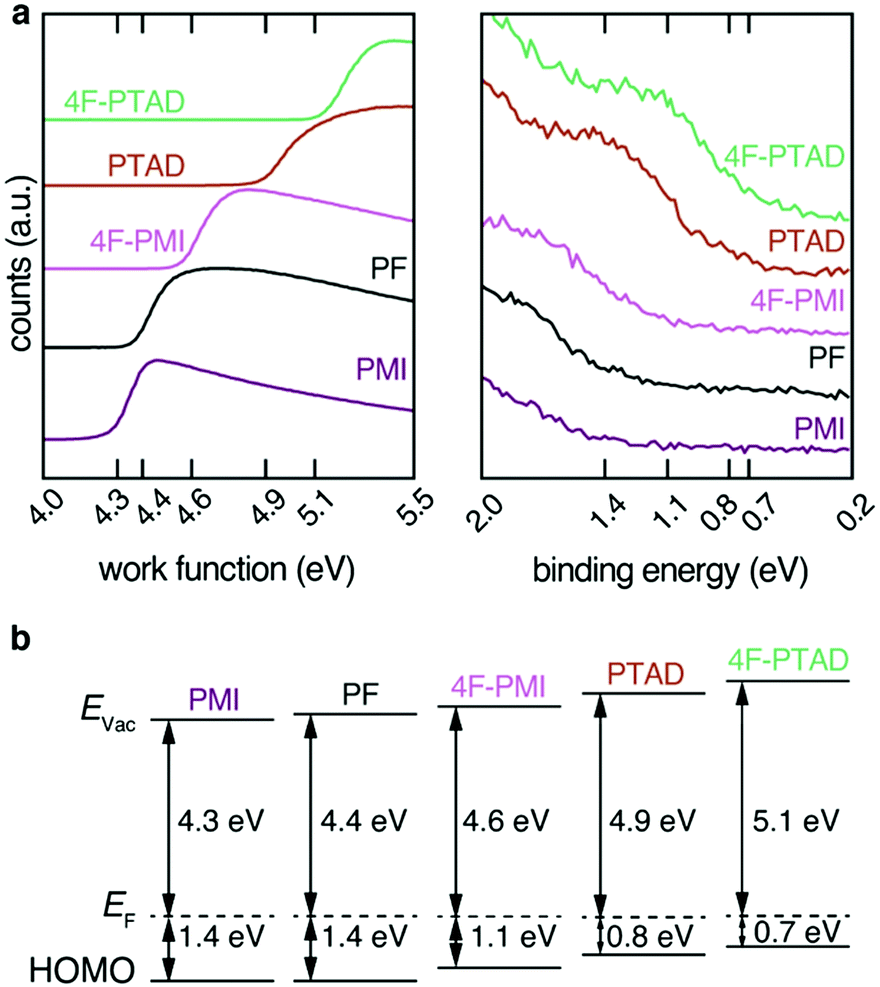 | ||
| Fig. 3 (a) Secondary electron cut-off and valence band onset (w.r.t. EF = 0 eV) of PF films for spin-coated PF and PF cross-linked and treated with dienophiles rounded to the significant digit. With increasing number of electronegative elements in the covalently bound dienophiles and therefore increasing electron affinity, a shift of the bands of the photoelectron spectra to higher energy is observed. (b) Energy levels as extracted from the UPS experiments. The observed shift in the photoelectron spectra translates into the increase of the work function and the decrease of the hole injection barrier of the films. | ||
Conversely, for each dienophile studied, the valence band showed a shift towards Fermi energy by the same absolute value as seen in the WF shift: PMI did not change the HIB of PF, followed by 4F-PMI, PTAD and 4F-PTAD, which showed the strongest HIB decrease from 1.4 eV to 0.7 eV. As a result of this equal WF increase and HIB decrease, the IP of all the functionalized series remained the same at 5.8 eV (within an experimental error of ±0.1 eV). All these values are schematically depicted in Fig. 3b. It must also be noted that the valence bands showed no additional features upon implementation of the dienophile molecules. The resulting WF and VB shifts are therefore only due to the functionalization process and no additional effects are observed. This can be seen in more detail in Fig. S8 (ESI†) for the most pronounced shift. The increase in work function of the films correlates with the increasing electron affinity of the dienophiles derived by DFT calculations (Fig. S7a, ESI†). The observed shifts are related to charge transfer from the acceptor moiety to the polymer film to place the Fermi energy inside the gap of the acceptor moiety. This behavior is reported as Fermi level pinning at the introduced LUMO states of the acceptor moiety (Fig. S7b, ESI†).5,16,32
Control experiments to test the influence of varying the reaction temperature, working in ambient conditions were conducted with 4F-PTAD. To exclude the possibility of the changes being due to an adsorbed layer of dienophile non-covalently bound to the polymer, the crosslinked film functionalized with 4F-PTAD was sonicated in toluene. This treatment did not alter the energy levels of the functionalized film (see Fig. S9, ESI†) proving that the dienophile was chemically bound to the PF film. The reactivity of 4F-PTAD was sufficient to carry out the functionalization experiment even at room temperature (RT). Energy levels of 4F-PTAD functionalized films determined at RT were equal to those achieved after functionalization at 100 °C (see Fig. S10, ESI†). To test the influence of environmental conditions on the process, the treatment with 4F-PTAD was performed under ambient conditions resulting in no difference in the energy levels (see Fig. S11, ESI†). This is in contrast to the cross-linked sample that was p-doped by exposure to ambient conditions, exposure of 4F-PTAD treated samples to ambient conditions has no detectable effect on the energy levels. Additionally, scanning force microscopy images (Fig. S12 and S13, ESI†) show negligible changes after cross-linking and treatment of the PF films, proving successful crosslinking and solvent resistance.
The above presented combination of cross-linking and subsequent functionalization therefore efficiently introduces spatially defined functional molecules at the surface; even at room temperature and in ambient conditions. The findings affirm the suggested picture of covalently attached acceptor sites modulating the energy levels of the treated films. Since the covalent anchoring at organic semiconductor interfaces has now been established, the design and synthesis of dienophiles with enhanced acceptor/donor properties will be targeted.
Conclusions
We have offered a protocol for the covalent interface functionalization of a solution-processed organic polymeric semiconductor. Four dienophiles have been covalently bound to cross-linked polyfluorene interfaces by Diels–Alder reactions. Surface functionalization was proven by an Ar+-sputter experiment and subsequent XPS measurement. The work function of the dienophile-treated films increased with increasing electron affinity of the dienophile. This can be attributed to Fermi level pinning at the LUMO of the acceptor at the interface. Ultimately, the presented process enables modular, covalent, spatially defined post-deposition functionalization of solution-processed organic polymeric semiconductors, important for tailor-made metal–organic and organic–organic interfaces as well as sensing applications. By designing dienophiles with a higher electron affinity, the acceptor effect of the anchoring molecules could be even more enhanced. Further studies will incorporate the best dienophiles into working devices to address challenges like the control of recombination zones at organic–organic interfaces or reduction of ohmic losses at metal–organic interfaces. Further investigations on the basis of the dienophile anchors will include synthesis of dienophiles carrying redox-active sites to enable spatially resolved doping in multilayer organic semiconductor-based devices such as OLEDs and organic and hybrid solar cells.The concept may further be used to covalently immobilize specific binding sites at the analyte/organic semiconductor interface for (bio)sensing applications. Introducing additional soft lithographic printing and transfer processes in the interface functionalization step will also offer the possibility of adding lateral spatial resolution to the concept. Alternatively, local heating based on surface probe microscopy methods or locally and selectively triggered Diels–Alder by electron beam can be used. All these applications are not limited to polyfluorene-based systems, but can be widely applied to numerous semi-conducting polymers such as high-performance donor–acceptor polymers: cross-linkable groups via highly selective, benign and widely applicable cycloadditions (cyclopentadienes, maleimides/furanes or anthracene-based systems) are easily introduced and generally tolerant towards a large variety of cross-coupling conditions employed for polymer synthesis.33–37 Though the present work necessitates dienyl-functionalized semiconductors (such functionalization should be feasible with the majority of semiconducting polymers), our concept should not be limited to Diels–Alder reactions, but also be transferable to other selective or even unspecific reactions utilized for cross-linking such as thiol–ene click reactions or oxirane-based cationic ring-opening polymerizations,38–42 as long as the semiconducting layer is (a) sufficiently solvent resistant towards the solution the dopant is applied from and (b) free reaction sites at the material interface are available. Overall, enabling covalent organic–organic interface functionalization from solution has great potential due to the scalability and cost effectiveness.
Conflicts of interest
There are no conflicts to declare.Acknowledgements
The authors acknowledge the support of the German Federal Ministry of Education and Research (BMBF) through Grant No. FKZ 13N13695 (POESIE), as well as support from the Helmholtz Energy Materials Foundry (HEMF) and PEROSEED (ZT-0024) project. This work was carried out in the framework of the Joint Lab GEN_FAB. The authors would also like to thank Minh Hai Nguyen and Paul Zybarth for technical assistance.Notes and references
- F. Tao and S. L. Bernasek, Functionalization of Semiconductor Surfaces, Wiley, Hoboken, New Jersey, 2012 Search PubMed.
- B. Lüssem, M. Riede and K. Leo, Phys. Status Solidi, 2013, 210, 9–43 CrossRef.
- R. Schlesinger, Y. Xu, O. T. Hofmann, S. Winkler, J. Frisch, J. Niederhausen, A. Vollmer, S. Blumstengel, F. Henneberger, P. Rinke, M. Scheffler and N. Koch, Phys. Rev. B, 2013, 87, 1–5 CrossRef.
- I. Salzmann, G. Heimel, M. Oehzelt, S. Winkler and N. Koch, Acc. Chem. Res., 2016, 49, 370–378 CrossRef CAS PubMed.
- M. Oehzelt, N. Koch and G. Heimel, Nat. Commun., 2014, 5, 4174 CrossRef CAS PubMed.
- S. Casalini, C. A. Bortolotti, F. Leonardi and F. Biscarini, Chem. Soc. Rev., 2017, 46, 40–71 RSC.
- F. S. Benneckendorf, S. Hillebrandt, F. Ullrich, V. Rohnacher, S. Hietzschold, D. Jänsch, J. Freudenberg, S. Beck, E. Mankel, W. Jaegermann, A. Pucci, U. H. F. Bunz and K. Müllen, J. Phys. Chem. Lett., 2018, 9, 3731–3737 CrossRef CAS PubMed.
- R. S. Williams, Comput. Sci. Eng., 2017, 19, 7–13 Search PubMed.
- J. M. Shalf and R. Leland, Computer, 2015, 48, 14–23 Search PubMed.
- D. A. Muller, Nat. Mater., 2005, 4, 645–647 CrossRef CAS PubMed.
- Y. Van De Burgt, A. Melianas, S. T. Keene, G. Malliaras and A. Salleo, Nat. Electron., 2018, 1, 386–397 CrossRef.
- J. S. Chang, A. F. Facchetti and R. Reuss, IEEE J. Emerg. Sel. Top. Circuits Syst., 2017, 7, 7–26 Search PubMed.
- L. Qiu, W. H. Lee, X. Wang, J. S. Kim, J. A. Lim, D. Kwak, S. Lee and K. Cho, Adv. Mater., 2009, 21, 1349–1353 CrossRef CAS.
- D. Guo, K. Sakamoto, K. Miki, S. Ikeda and K. Saiki, Appl. Phys. Lett., 2007, 90, 102117 CrossRef.
- I. Salzmann and G. Heimel, J. Electron Spectrosc. Relat. Phenom., 2015, 204, 208–222 CrossRef CAS.
- A. Opitz, J. Phys.: Condens. Matter, 2017, 29, 133001 CrossRef PubMed.
- I. E. Jacobs and A. J. Moulé, Adv. Mater., 2017, 29, 1–39 Search PubMed.
- Y. Qi, T. Sajoto, S. Barlow, E.-G. Kim, J.-L. Brédas, S. R. Marder and A. Kahn, J. Am. Chem. Soc., 2009, 131, 12530–12531 CrossRef CAS PubMed.
- Y. Zhang, B. De Boer and P. W. M. Blom, Phys. Rev. B, 2010, 81, 1–5 Search PubMed.
- S. Sax, N. Rugen-Penkalla, A. Neuhold, S. Schuh, E. Zojer, E. J. W. List and K. Müllen, Adv. Mater., 2010, 22, 2087–2091 CrossRef CAS PubMed.
- R. Trattnig, L. Pevzner, M. Jäger, R. Schlesinger, M. V. Nardi, G. Ligorio, C. Christodoulou, N. Koch, M. Baumgarten, K. Müllen and E. J. W. List, Adv. Funct. Mater., 2013, 23, 4897–4905 CrossRef CAS.
- S. Nau, N. Schulte, S. Winkler, J. Frisch, A. Vollmer, N. Koch, S. Sax and E. J. W. List, Adv. Mater., 2013, 25, 4420–4424 CrossRef CAS PubMed.
- H.-J. Gossmann and E. F. Schubert, Crit. Rev. Solid State Mater. Sci., 1993, 18, 1–67 CrossRef CAS.
- J. Li, C. W. Rochester, I. E. Jacobs, S. Friedrich, P. Stroeve, M. Riede and A. J. Moulé, ACS Appl. Mater. Interfaces, 2015, 7, 28420–28428 CrossRef CAS PubMed.
- K. Walzer, B. Maennig, M. Pfeiffer and K. Leo, Chem. Rev., 2007, 107, 1233–1271 CrossRef CAS PubMed.
- P. Reiser, F. S. Benneckendorf, M. M. Barf, L. Müller, R. Bäuerle, S. Hillebrandt, S. Beck, R. Lovrincic, E. Mankel, J. Freudenberg, D. Jänsch, W. Kowalsky, A. Pucci, W. Jaegermann, U. H. F. Bunz and K. Müllen, Chem. Mater., 2019, 31, 4213–4221 CrossRef CAS.
- L. Ahrens, S. Schlisske, K.-P. Strunk, F. Hinkel, C. Melzer, U. H. F. Bunz, U. Lemmer, G. Hernandez-Sosa, D. Jänsch, J. Freudenberg and K. Müllen, Chem. Mater., 2018, 30, 4157 CrossRef CAS.
- A. Sanyal, Macromol. Chem. Phys., 2010, 211, 1417–1425 CrossRef CAS.
- P. J. Brewer, J. Huang, P. A. Lane, A. J. DeMello, D. D. C. Bradley and J. C. DeMello, Phys. Rev. B, 2006, 74, 2–7 CrossRef.
- V. D. Kiselev, D. A. Kornilov, I. I. Lekomtseva and A. I. Konovalov, Int. J. Chem. Kinet., 2015, 47, 289–301 CrossRef CAS.
- M. A. Tasdelen, Polym. Chem., 2011, 2, 2133–2145 RSC.
- M. Oehzelt, K. Akaike, N. Koch and G. Heimel, Sci. Adv., 2015, 1, e1501127 CrossRef PubMed.
- S. Holliday, Y. Li and C. K. Luscombe, Prog. Polym. Sci., 2017, 70, 34–51 CrossRef CAS.
- D. G. Patel, K. R. Graham and J. R. Reynolds, J. Mater. Chem., 2012, 22, 3004–3014 RSC.
- T. Brand and M. Klapper, Des. Monomers Polym., 1999, 2, 287–309 CrossRef CAS.
- J. R. Jones, C. L. Liotta, D. M. Collard and D. A. Schiraldi, Macromolecules, 1999, 32, 5786–5792 CrossRef CAS.
- Y. Zheng, M. Micic, S. V. Mello, M. Mabrouki, F. M. Andreopoulos, V. Konka, S. M. Pham and R. M. Leblanc, Macromolecules, 2002, 35, 5228–5234 CrossRef CAS.
- C. E. Hoyle and C. N. Bowman, Angew. Chem., Int. Ed., 2010, 49, 1540–1573 CrossRef CAS PubMed.
- M. Casutt, M. Ruscello, N. Strobel, S. Koser, U. H. F. Bunz, D. Jänsch, J. Freudenberg, G. Hernandez-Sosa and K. Müllen, Chem. Mater., 2019, 31, 7657–7665 CrossRef CAS.
- M. S. Bayerl, T. Braig, O. Nuyken, D. C. Müller, M. Groß and K. Meerholz, Macromol. Rapid Commun., 1999, 20, 224–228 CrossRef CAS.
- E. Bacher, S. Jungermann, M. Rojahn, V. Wiederhirn and O. Nuyken, Macromol. Rapid Commun., 2004, 25, 1191–1196 CrossRef CAS.
- C. D. Müller, A. Falcou, N. Reckefuss, M. Rojahn, V. Wiederhirn, P. Rudati, H. Frohne, O. Nuyken, H. Becker and K. Meerholz, Nature, 2003, 421, 829–833 CrossRef PubMed.
Footnote |
| † Electronic supplementary information (ESI) available: Supplementary XPS and UPS figures, DFT calculations, and experimental methods. See DOI: 10.1039/c9tc06180k |
| This journal is © The Royal Society of Chemistry 2020 |