
 Open Access Article
 This Open Access Article is licensed under a
 Creative Commons Attribution 3.0 Unported Licence
Strengthened relaxor behavior in (1−x)Pb(Fe0.5Nb0.5)O3–xBiFeO3†
Uroš
Prah
ab,
Mirela
Dragomir
a,
Tadej
Rojac
ab,
Andreja
Benčan
ab,
Rachel
Broughton
c,
Ching-Chang
Chung
d,
Jacob L.
Jones
c,
Rachel
Sherbondy
e,
Geoff
Brennecka
 e and
Hana
Uršič
*ab
e and
Hana
Uršič
*ab
aJožef Stefan Institute, Jamova cesta 39, 1000 Ljubljana, Slovenia. E-mail: hana.ursic@ijs.si
bJožef Stefan International Postgraduate School, Jamova cesta 39, 1000 Ljubljana, Slovenia
cDepartment of Materials Science and Engineering, North Carolina State University, Raleigh, NC 27695, USA
dAnalytical Instrumentation Facility, North Carolina State University, Raleigh, NC 27695, USA
eColorado School of Mines, 1500 Illinois St., Golden, CO 80401, USA
First published on 10th February 2020
Abstract
A systematic study of (1−x)Pb(Fe0.5Nb0.5)O3–xBiFeO3 (x = 0–0.5) was performed by combining dielectric and electromechanical measurements with structural and microstructural characterization in order to investigate the strengthening of the relaxor properties when adding BiFeO3 into Pb(Fe0.5Nb0.5)O3 and forming a solid solution. Pb(Fe0.5Nb0.5)O3 crystalizes in monoclinic symmetry exhibiting ferroelectric-like polarization versus electric field (P–E) hysteresis loop and sub-micron-sized ferroelectric domains. Adding BiFeO3 to Pb(Fe0.5Nb0.5)O3 favors a pseudocubic phase and a gradual strengthening of the relaxor behavior of the prepared ceramics. This is indicated by a broadening of the peak in temperature-dependent permittivity, narrowing of P–E hysteresis loops and decreasing size of ferroelectric domains resulting in polar nanodomains for x = 0.20 composition. The relaxor behavior was additionally confirmed by Vogel–Fulcher analysis. For the x ≥ 0.30 compositions, broad high-temperature anomalies are observed in dielectric permittivity versus temperature measurements in addition to the frequency-dispersive peak located close to room temperature. These samples also exhibit pinched P–E hysteresis loops. The observed pinching is most probably related to the reorganization of polar nanoregions under the electric field as shown by synchrotron X-ray diffraction measurements as well as by piezo-response force microscopy analysis, while in part affected by the presence of charged point defects and anti-ferroelectric order, as indicated from rapid cooling experiments and high-resolution transmission electron microscopy, respectively.
I. Introduction
BiFeO3 (BFO)1,2 and Pb(Fe0.5Nb0.5)O3 (PFN)3–5 are two of the most known and well-studied single-phase multiferroics, in which ferroelectric and antiferromagnetic orders can coexist. BFO exhibits a paraelectric–ferroelectric phase transition at 825 °C, known as the ferroelectric Curie temperature (TC), and a paramagnetic–antiferromagnetic phase transition at 370 °C, denoted as the magnetic Néel temperature (TN).1 In PFN, both TC and TN occur at much lower temperatures, i.e., ∼100 °C and −120 °C, respectively.4,6According to the literature reports, there is still a debate about whether PFN exhibits more ferroelectric-like or relaxor-like behavior.4,7–9 At room temperature, it exhibits a monoclinic symmetry with Cm space group10 exhibiting ferroelectric-like P–E hysteresis loops11 and sub-micron-sized ferroelectric domains.8,10 It possesses frequency independent (or only slightly dependent, i.e., ±1 °C) peak-permittivity temperature for frequencies below 1 MHz.11,12 However, it was shown12 that the peak-permittivity temperature becomes frequency dependent in the microwave frequency region (GHz), indicating partial relaxor-like behavior. On the other hand, BFO shows ferroelectric behavior at room temperature and is also considered a high-temperature piezoelectric material due to its extremely high TC.13 What about the PFN–BFO solid solutions? Are they showing more ferroelectric- or relaxor-like behaviors at room temperature? This open question will be answered in this paper.
The preparation of different (1−x)Pb(Fe0.5Nb0.5)O3–xBiFeO3 (PFN–100xBFO) solid solutions was demonstrated in the 1960s14–17 and many other studies followed, all using classical solid-state synthesis.18–25 Most of these reports focused on BFO-rich PFN–100xBFO (x ≥ 0.5) compositions and investigation of their magnetic properties. However, as shown in this work, PFN-rich compositions (x < 0.5) exhibit an interesting ferroelectric-relaxor behavior that is strengthened by adding BFO to PFN.
Large dielectric permittivity values across a broad temperature range, large electrostriction coefficients, low hysteresis losses and large change of field-induced polarization makes relaxors useful for capacitors, energy storage applications,26 precision displacement actuators, transducers26,27 and electrocaloric cooling elements.28 One of the reasons that the ferroelectric-relaxor behavior has not yet been reported in PFN–BFO system may lay in the challenging preparation of single-phase ceramics with low electrical conductivity.
In this work, seven PFN–100xBFO (x = 0, 0.05, 0.1, 0.2, 0.3, 0.4 and 0.5) compositions were prepared by mechanochemical synthesis followed by sintering. This synthesis route has proven useful for the preparation of complex single-phase ceramics due to the better chemical homogeneity and partial amorphization of mechanochemically-activated powder, which can lead to lower sintering temperatures and more homogeneous and stoichiometric ceramics.11,29,30 We show in this study that PFN–100xBFO (x ≤ 0.5) is an interesting system exhibiting relaxor-like behavior. Electrical properties of ferroelectrics and relaxors are strongly dependent on the grain size of the material.31,32 Therefore, in this work special attention was given in order to prepare all samples with similar grain size. Local domain structure was investigated at the sub-micron scale in addition to macroscopic measurements of dielectric permittivity and losses, polarization– and strain–electric field hysteresis loops and piezoelectric properties. The strengthened relaxor behavior by addition of BFO to PFN is therefore reported in detail here for the first time.
II. Experimental
A. Material synthesis
PFN–100xBFO (x = 0, 0.05, 0.1, 0.2, 0.3, 0.4 and 0.5) ceramic powders were prepared by mechanochemical-activation-assisted synthesis using PbO (99.9%, Alfa Aesar), Fe2O3 (99.9%, Alfa Aesar), Nb2O5 (99.9%, Aldrich) and Bi2O3 (99.999%, Alfa Aesar) as starting oxides. The preparation process of pure Pb(Fe0.5Nb0.5)O3 (PFN) powder is described in our previous work.11 Prior to the preparation of BFO-containing compositions, all starting oxides were pre-milled in absolute ethanol using a planetary ball mill (Retsch PM400, Retsch, Haan, Germany) at 200 min−1 for 4–6 h or an attrition mill (Netzsch, PE075/PR01, Selb, Germany) at 500 min−1 for 6–8 h. In all cases, yttria-stabilized zirconia (YSZ) milling balls with a diameter of 3 mm were used. All stoichiometric mixtures of starting oxides (40 g) were homogenized in a planetary ball mill at 200 min−1 for 4 h in absolute ethanol using YSZ milling balls (ball diameters 3 mm). The homogenized mixtures were then dried and mechanochemically activated in the same planetary ball mill for 14 h at 400 min−1 in a tungsten carbide milling vial (volume 80 cm3), filled with 7 tungsten carbide milling balls (ball diameters 15 mm). After activation, the synthesized powders, i.e., mixtures of crystalline perovskite and amorphous phases (ESI† material, A), were re-milled in a planetary ball mill in absolute ethanol, at 200 min−1, for 4 h, using YSZ milling balls (ball diameters 3 mm).All prepared powders were uniaxially pressed (50 MPa) into pellets of a diameter of 8 mm followed by isostatic pressing at 300 MPa. The powder compacts were reactively sintered in double alumina crucibles in the presence of PFN packing powder. Sintering temperatures for each composition were estimated from sintering curves (details in ESI† material, B). In order to maintain similar grain size in all compositions (ESI† material, C), two different sintering temperatures were used. PFN–100xBFO samples with lower content of BFO (x = 0, 0.05 and 0.1) were sintered at 950 °C for 2 h, while samples with higher content of BFO (x = 0.2, 0.3, 0.4 and 0.5) were sintered 50 °C lower, i.e., 900 °C. Sintering runs were performed in oxygen atmosphere as suggested in ref. 33 and used in our previous work.11 The use of saturated oxygen atmosphere during the sintering prevents (or minimizes) the reduction of Fe3+ to Fe2+ and reduces the amount of oxygen vacancies, which consequently resulted in a lower electrical conductivity and dielectric losses of the material.33 For all samples, heating and cooling rates of 2 °C min−1 were used.
B. Characterization
The densities of the sintered pellets were determined using a gas-displacement density analyzer (Micromeritics, AcuuPyc II 1340 Pycnometer) at room temperature (RT). For the calculation of the relative density of PFN, the crystallographic density of 8.46 g cm−3 was used (PDF card no. 032-0522),34 while for other compositions, crystallographic densities were obtained from Rietveld refinement analysis (details in ESI† material, D).X-ray powder diffraction (XRD) patterns of crushed ceramic pellets were recorded on a X’Pert Pro (PANalytical B.V., Netherlands) high-resolution powder diffractometer equipped with Cu Kα1 radiation (45![[thin space (1/6-em)]](https://www.rsc.org/images/entities/char_2009.gif) kV, 40mA), in reflection mode. Diffraction patterns were recorded in the 15–120° 2θ-range with a step size of 0.008° and an integration time of 100 s per step at RT. The phase identification was done with PDF-4+ database.
kV, 40mA), in reflection mode. Diffraction patterns were recorded in the 15–120° 2θ-range with a step size of 0.008° and an integration time of 100 s per step at RT. The phase identification was done with PDF-4+ database.
The quantitative phase composition analyses were performed using the Rietveld refinement method. The Topas R package (version 2.1, Bruker, AXS, Karlsruhe, Germany) was employed and a Fundamental Parameters Approach was used to describe the peak profile.35 In this model, the background (10th order Chebychev), unit cell parameters, crystallite size, scale factors, sample displacement, atomic coordinates, and thermal parameters were stepwise refined to obtain a calculated diffraction profile that best fits the experimental pattern. The quality of the fit was assessed from the goodness-of-fit parameters Rwp, Rp, Rexp, RB, and G.O.F.
Electric field dependent synchrotron X-ray diffraction (sXRD) was conducted at the 11-ID-C beamline of the Advanced Photon Source (APS) at Argonne National Laboratory (Lemont, IL, USA). The wavelength used for the sXRD experiments was 0.1173 Å. Diffraction data for PFN–100xBFO (x = 0.4 and 0.5) were measured during application of various field amplitudes (from 0 to 5 kV cm−1 in 0.5 kV cm−1 increment) and after release from electric field (0 kV cm−1). The diffraction profiles represent scattering vectors oriented approximately parallel to the electric field. Debye–Scherrer rings of the samples under each electric field were measured with an exposure time of 0.5 s for 100 frames using a 2D PerkinElmer area detector. After that, a 1D pattern was calculated with FIT2D software by integrating a 2D diffraction image over an azimuthal 20° sector along the direction of the applied electric field. The beam center and distance were calibrated using a CeO2 standard.
The microstructure of sintered ceramics was examined using a field-emission scanning electron microscope (FE-SEM, JSM-7600F, Jeol Ltd., Japan). Prior to microstructural analysis, the samples were fractured for fracture-surface examination, ground and fine-polished using a colloidal silica suspension, followed by thermal etching at 775 °C for 15 minutes in the presence of PFN packing powder. The average grain size and grain-size distribution were evaluated from the digitized images of etched surfaces, processed using the Image Tool software (UTHSCSA Image Tool Version 3.00. 2002)36 by measuring more than 500 grains. The grain size is expressed as the Feret's diameter.37 For the study of structural properties on the nanometer scale transmission electron microscope (TEM) JEM-2010F (Jeol Ltd., Japan) was used. TEM samples were prepared by mechanical grinding, dimpling and final Ar-ion milling.38
The local domain structure of sintered ceramics was recorded with an atomic force microscope (AFM, Asylum Research, Molecular Force Probe 3D, Santa Barbara, CA, USA) equipped with a piezoresponse force microscopy (PFM) dual AC resonance-tracking mode. Prior to the PFM measurements, surfaces of ceramic samples were prepared using standard metallographic procedures (thinning, grinding, polishing and fine polishing with SiO2 particles) followed by heat treatment at 600 °C for 1 h with a cooling rate of 1 °C min−1, in order to release internal stresses in the material. The final thicknesses of the as-prepared samples were ∼70 μm. A tetrahedral Si tip (curvature diameter of 30 ± 10 nm) on a Si cantilever, both coated with Ti/Ir (Asyelec, AtomicForce F&E GmbH, Mannheim, Germany), was used. PFM out-of-plane amplitude images were conducted by applying an AC voltage of 10 and 20 V between the tip and the bottom electrode.
For characterization of electrical properties, the ceramic pellets were cut, thinned and polished to a thickness of ∼200 μm (∼600 μm for strain loops). In order to release the internal stresses produced during the mechanical processing, the thinned ceramic pellets were heated up to 600 °C for 1 h (with 5 °C min−1 heating rate) and then slowly cooled down (1 °C min−1) to RT. The surfaces of the pellets were coated with Au electrodes (diameter of 5 mm) using RF-magnetron sputtering machine (5 Pascal, Italy). The relative dielectric permittivity (ε) and dielectric loss (tanδ) as a function of temperature were analyzed during cooling from 200 °C to −50 °C using an Aixacct TF analyzer 2000 (aixACCT Systems GmbH, Aachen, Germany) coupled with a HP 4284A (Hewlett-Packard, California, USA) Precision LCR impedance meter in a frequency range of 0.1–100 kHz. AC current density–electric field (J–E) and strain–electric field (S–E) loops were measured at RT using an Aixacct TF analyzer 2000 equipped with a laser interferometer by applying a single sinusoidal waveform with the frequency of 1 Hz (10 Hz for strain loops) and electric fields up to 70 kV cm−1. Polarization–electric field (P–E) loops were automatically obtained by software using numerical integration of current signal. Piezoelectric coefficient (d33) values were measured at RT and 100 Hz of stress frequency using a Berlincourt piezometer (Take Control PM10, Birmingham, UK). The measurements were performed 24 h after poling the samples. The results were presented in each composition as the mean value and standard deviation of the measurements done on three pellets. Prior to the measurements, the samples were poled in a silicone-oil bath at RT by applying a DC electric field of 30 kV cm−1 for 30 min.
III. Results and discussion
Firstly, the phase present, lattice parameters and microstructure of all seven PFN–100xBFO (x = 0–0.5) compositions were investigated. X-ray powder diffraction data indicate that all of the samples are pyrochlore-free, namely only the perovskite peaks are visible (see ESI,† material, D). Pure PFN crystallizes in monoclinic symmetry with Cm space group, which is in agreement with previous reports.10,39,40 Substituting PFN with BFO leads to the formation of a pseudocubic (space group Pm![[3 with combining macron]](https://www.rsc.org/images/entities/char_0033_0304.gif) m) phase as previously reported in ref. 14, 16 and 22. In compositions with smaller amounts of BFO (x = 0.05 and 0.1), Rietveld analysis revealed the coexistence of monoclinic and pseudocubic phases, while in samples with higher BFO contents (0.2 ≤ x ≤ 0.5) only a pseudocubic phase is present (Fig. 1a and b). According to the literature,14,16 a transformation from cubic to rhombohedral symmetry (space group R3c) takes place in compositions with x > 0.6. Phase composition and lattice constants of all prepared samples are schematically shown in the form of a PFN–BFO phase diagram, presented in Fig. 1c. Details of Rietveld refinement analysis are shown in ESI† material, D.
m) phase as previously reported in ref. 14, 16 and 22. In compositions with smaller amounts of BFO (x = 0.05 and 0.1), Rietveld analysis revealed the coexistence of monoclinic and pseudocubic phases, while in samples with higher BFO contents (0.2 ≤ x ≤ 0.5) only a pseudocubic phase is present (Fig. 1a and b). According to the literature,14,16 a transformation from cubic to rhombohedral symmetry (space group R3c) takes place in compositions with x > 0.6. Phase composition and lattice constants of all prepared samples are schematically shown in the form of a PFN–BFO phase diagram, presented in Fig. 1c. Details of Rietveld refinement analysis are shown in ESI† material, D.
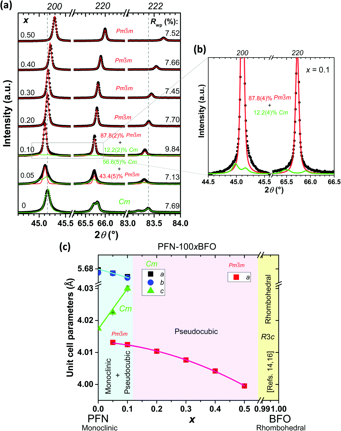 | ||
| Fig. 1 (a) Room-temperature XRD profiles of the 200, 220, and 222 pseudocubic reflections (only from Cu Kα1) for PFN–100xBFO (x = 0–0.5). The calculated profile for the monoclinic phase (Cm space group) is represented in green, while the pseudocubic phase (Pmm space group) is displayed in red. (b) Zoom-in patterns of 200 and 220 reflections of the PFN–10BFO composition show the scattering contribution of both Cm and Pmm phases to the diffraction pattern. (c) Lattice parameters of the PFN–100xBFO for compositions 0 ≤ x ≤ 0.5. | ||
Micrographs of polished and fractured sample surfaces are shown in Fig. 2. In all cases the microstructures are uniform, homogeneous and without the presence of visible secondary phases, which is in agreement with the results of the XRD analysis. All of the solid solutions are highly dense, from 97.6% to 99.7% of the theoretical density. The average grain size of all samples is comparable, i.e., between 0.8 and 1.4 μm (see Fig. 2). Monomodal grain size distributions indicate a normal grain growth during the sintering process (ESI† material, C).
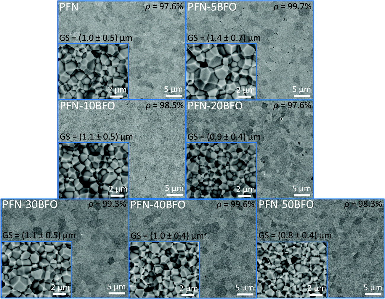 | ||
| Fig. 2 SEM micrographs of polished and fractured (insets) PFN–100xBFO (x = 0–0.5). | ||
The temperature and frequency (ν) dependence of the real component of relative permittivity ε′ and dielectric loss tan![[thin space (1/6-em)]](https://www.rsc.org/images/entities/i_char_2009.gif) δ for all compositions are shown in Fig. 3. In PFN, a paraelectric–ferroelectric phase transition with peak-permittivity values of ∼30000 (at 0.1 kHz) is observed at ∼113 °C, showing a diffuse phase transition with a weak relaxor-like frequency dispersion, in agreement with literature data.3,5,41,42 According to the high temperature of the paraelectric–ferroelectric phase transition in BFO (∼825 °C),1,2 it would be expected that the peak-permittivity temperature (Tε,max) of PFN–100xBFO system will be higher compared to PFN. Surprisingly, with a gradual increase in the BFO content up to x = 0.2, the Tε,max of PFN–100xBFO solid solutions decreases, and dielectric peaks become more diffuse and frequency dependent, which indicates a strengthening of the relaxor behavior of the material.
δ for all compositions are shown in Fig. 3. In PFN, a paraelectric–ferroelectric phase transition with peak-permittivity values of ∼30000 (at 0.1 kHz) is observed at ∼113 °C, showing a diffuse phase transition with a weak relaxor-like frequency dispersion, in agreement with literature data.3,5,41,42 According to the high temperature of the paraelectric–ferroelectric phase transition in BFO (∼825 °C),1,2 it would be expected that the peak-permittivity temperature (Tε,max) of PFN–100xBFO system will be higher compared to PFN. Surprisingly, with a gradual increase in the BFO content up to x = 0.2, the Tε,max of PFN–100xBFO solid solutions decreases, and dielectric peaks become more diffuse and frequency dependent, which indicates a strengthening of the relaxor behavior of the material.
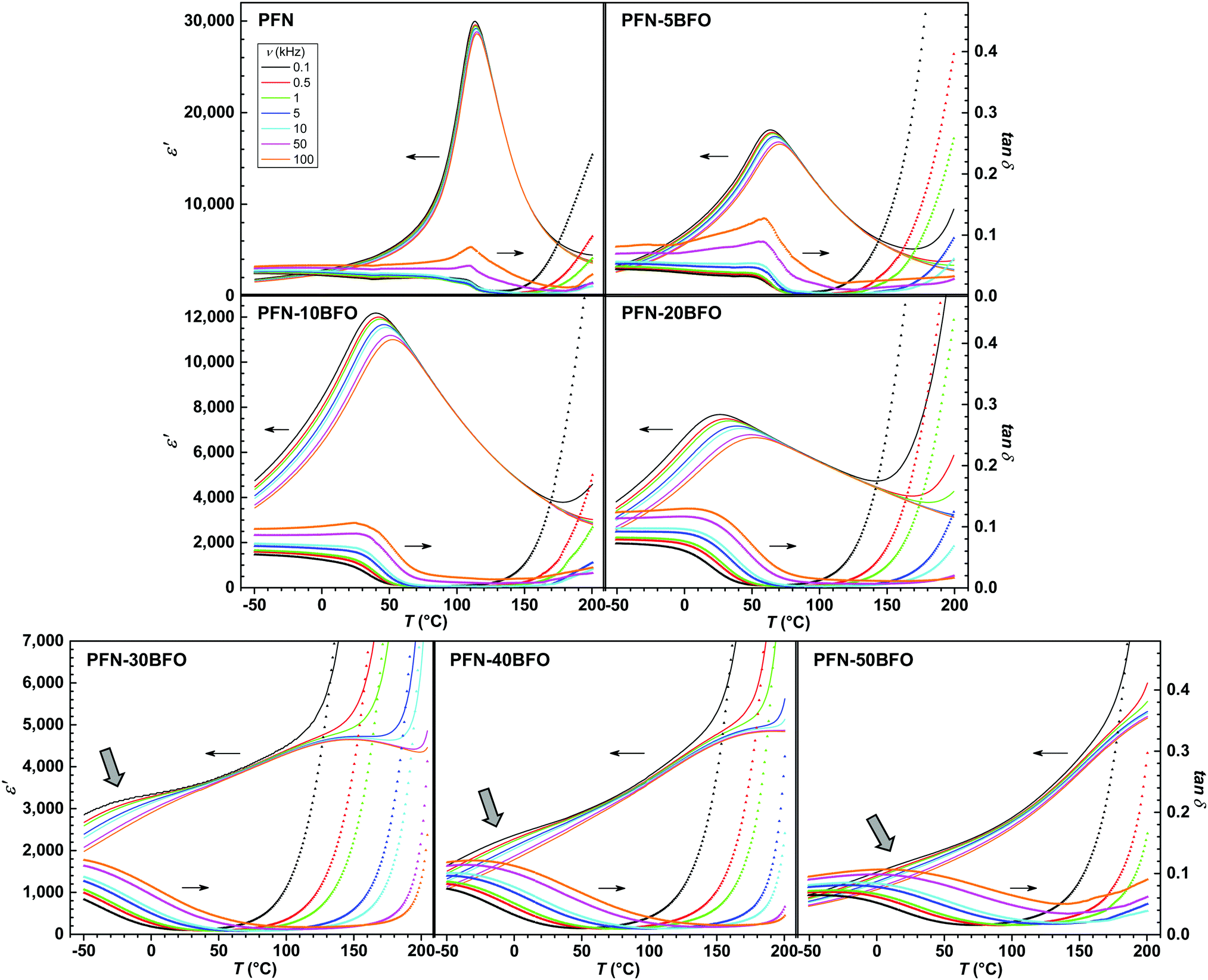 | ||
| Fig. 3 Temperature and frequency dependences of ε′ and tanδ of PFN–100xBFO (x = 0–0.5). Note the differences in scales of ε′. | ||
Increasing relaxor behavior is clearly evident in the frequency dependence of a Tε,max (Fig. 4a). The Tε,max reaches the lowest value of 26 °C (at 0.1 kHz) in PFN–20BFO. In Fig. 4b the ΔTε,maxversus the sample composition is shown, where ΔTε,max is defined as a difference between Tε,max at 0.1 kHz and 100 kHz. ΔTε,max is usually used to represent the relaxor behavior of the material.43 As it can be seen, ΔTε,max increases with addition of BFO with the maximum ΔTε,max of 26 °C obtained in PFN–20BFO sample.
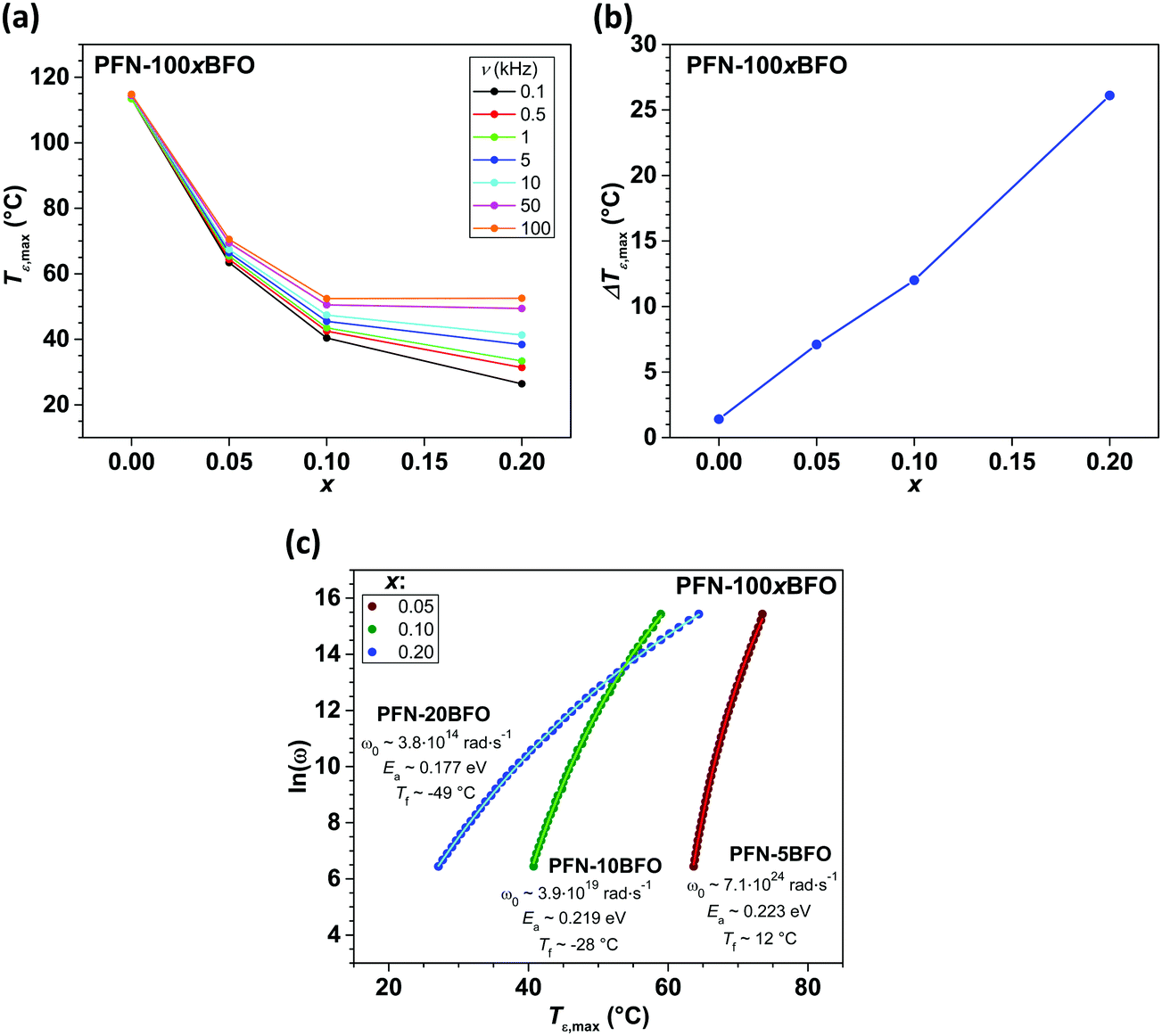 | ||
| Fig. 4 (a) Frequency dependence of Tε,max, (b) ΔTε,max and (c) Tε,maxversus ln(ω) relations of PFN–100xBFO (x = 0–0.2). Line curves in (c) show the fits to our data using the V–F equation (see text) from where the ω0, Ea and Tf parameters were obtained. Due to a too high electrical conductivity contribution, the values for x = 0.3–0.5 compositions could not be determined. | ||
To further confirm the relaxor behavior of x ≤ 0.2 compositions, Vogel–Fulcher analysis of ε′ (T, ν) data was performed. The origin of the frequency-dispersive peak-permittivity of relaxors is related to the dynamics of polar nanoregions that freeze at the so-called freezing temperature (Tf).44,45 The relationship between Tf, Tε,max and driving frequency of the applied external electric field can be described with Vogel–Fulcher (V–F) relation, ω = ω0exp[−Ea/kb(Tε,max − Tf)], where Ea represents activation energy, kb is Boltzmann constant, ω (2πν) is angular frequency and ω0 is a characteristic frequency.45–47Tε,max(ω) relations of 0 < x ≤ 0.20 compositions were fitted with V–F equation, where three parameters (ω0, Ea and Tf) were obtained (Fig. 4c). The fitting formalism and the adequacy of our experimental data were validated on a well-known and studied Pb(Mg1/3Nb2/3)O3 relaxor material (ESI† material, E).
Frequency-dependent dielectric permittivity responses of x = 0.05, 0.10 and 0.20 compositions nicely fit the V–F relation, confirming the relaxor behavior of these samples. The values of V–F parameters obtained by fitting, are shown in Fig. 4c. The Tf as well as Ea decreased with increasing the amount of BFO (up to x = 0.20), in agreement with the strengthening of relaxor behavior in these samples. It looks that the incorporation of BFO into the PFN crystal lattice stabilizes an ergodic relaxor phase. The reason for that could be related with an increased structural disorder, when different multivalence ions, such as Pb2+ and Bi3+, occupy a crystallographically equivalent A-site of the perovskite structure.26,48
When increasing the BFO content (x = 0.3, 0.4 and 0.5), a more complex dielectric response is present. Slightly below or close to RT, a likely dispersive anomaly that could be related to traces of the frequency-dependent response seen in x ≤ 0.2 compositions, is observed (marked by arrows in Fig. 3). On the other hand, it seems that in these compositions an additional anomaly starts to appear at temperatures higher than the permittivity maximum of pure PFN (Fig. 3). For PFN–30BFO this Tε,max is observed at ∼150 °C, while for PFN–40BFO and PFN–50BFO, at ∼200 °C and >200 °C, respectively. Due to the increased electrical conductivity at higher temperatures, which is also evident in the large increase of tanδ with temperature (Fig. 3), a more precise determination of the Tε,max in these compositions was not possible.
To further investigate the origin of likely non-dispersive high temperature maximum of dielectric permittivity, differential scanning calorimetry (DSC) measurements were employed (ESI† material, F). DSC measurements of PFN–100xBFO (x = 0.3, 0.4 and 0.5) revealed an endothermic anomaly located in the vicinity of the peak-permittivity temperature, which might indicate a structural (anti)polar-to-non-polar phase transition. However, no detectable structural changes were observed in high-temperature XRD data (ESI† material, G).
A similar trend of Tε,max behavior was observed in ref. 14, 16 and 22, however the reported ε′ values are much lower in comparison to the ones shown in Fig. 3. Furthermore, ε′ were reported only at high frequencies (MHz range), most probably due to the high electrical conductivity of samples prepared by classical solid-state synthesis.14,16 A possible reason for these differences could be a better chemical homogeneity and stoichiometry of mechanochemically-activated powder compared to those prepared by solid-state synthesis, as previously suggested for PFN11 and Pb(Sc0.5Nb0.5)O3.30
The tanδ values generally increase with increasing the BFO content (Fig. 3), are frequency-dependent and relatively low at the temperatures below 100 °C, namely 0.03 to 0.10 in a range between 0.1 and 100 kHz. The anomalies observed in tanδ of PFN–100xBFO samples are correlated with the peak-permittivity values. Above 120 °C, the tanδ increases with increasing temperature for all compositions. Comparison with previous reports is not possible due to the lack of given data or very high electrical conductivity of previously reported PFN–BFO samples.14,16,22
In order to verify the progressively increased relaxor behavior by the addition of BFO and to clarify the reason for the appearance of high-temperature anomaly observed by dielectric spectroscopy and DSC, the local structure of the samples was investigated using transmission electron microscopy (TEM). TEM micrographs of three solid solutions, i.e., PFN, PFN–20BFO and PFN–50BFO, are shown in Fig. 5. In PFN, sub-micrometer-large wedge-type domains (marked by red arrows in Fig. 5a) indicate a more ferroelectric nature of the sample. On the other hand, in PFN–20BFO and PFN–50BFO only areas with nano-sized patterns (marked by green dashed circles in Fig. 5b and c) were observed.
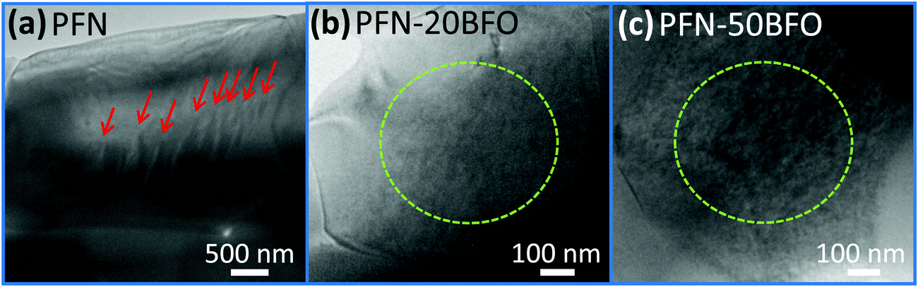 | ||
| Fig. 5 TEM images of (a) PFN, (b) PFN–20BFO and (c) PFN–50BFO solid solutions. Sub-micron-sized wedge-type domains and nano-sized patterns are marked by red arrows and green dashed circles, respectively. | ||
The local short-range ordering was further investigated using high-resolution TEM (HRTEM). HRTEM image of PFN–50BFO with corresponding Fast Fourier Transform (FFT) is shown in Fig. 6a. FFT reveals superlattice ½ ½ 0 reflections or so-called α spots.49,50 Inverse FFT image using α spots (Fig. 6b) shows ∼5 nm large regions whose origin could be related to anti-ferroelectric (AFE) fluctuations as already explained by A. Tkachuk et al.50 However, it seems that the amount of the nano-AFE regions embedded in the pseudocubic relaxor phase is too small to be detected by XRD. HRTEM analyses were additionally performed for PFN–20BFO sample, but no α spots were found (ESI† material, H). The presence of AFE order could be the reason for the occurrence of high-temperature anomalies observed in dielectric permittivity measurements. These findings are supported by the results of the DSC analysis, where in PFN-rich compositions (x ≤ 0.2) no anomalies were seen, while in BFO-rich compositions (x ≥ 0.3) high-temperature phase changes were detected.
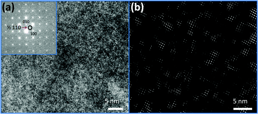 | ||
| Fig. 6 (a) HRTEM image of a PFN–50BFO grain in [001] zone axis. Inset shows the FFT that reveals diffuse ½ ½ 0 type spots (marked with red arrow). (b) The inverse FFT image using diffuse spots only highlights up to 5 nm large regions. | ||
The local ferroelectric domain structure was additionally studied by piezoresponse force microscopy (PFM). PFM out-of-plane amplitude images, scanned at an AC drive amplitude of 10 V (the first scan of a virgin area) and 20 V, are shown in Fig. 7a and b, respectively. In PFN long-range ferroelectric order, evidenced by a sub-micrometer-large domain structure, was observed. Two different types of sub-micron-sized domains, wedged (marked by blue dashed arrows in Fig. 7a) and irregularly shaped (green dotted arrows in Fig. 7a) were also observed, in agreement a with previous study.10 With increasing the amount of BFO, long-range ferroelectric domains gradually disappear. In the PFN–5BFO composition, irregularly shaped domains become smaller, a few hundred nm in size, and more rounded (marked by red solid arrows in Fig. 7a). In the PFN–10BFO composition, a PFM signal is still detected, but the size of irregular domains drops to a few tens of nanometers (marked by orange open arrows in Fig. 7a), which is close to the resolution limit of the PFM technique. In compositions with higher amounts of BFO (x ≥ 0.2) zero piezo-response signal was observed at an AC drive amplitude of 10 V. These results are consistent with the TEM study, where in PFN–50BFO only nano-range ordering is observed that is below the PFM detection limit (tip diameter ∼30 nm).
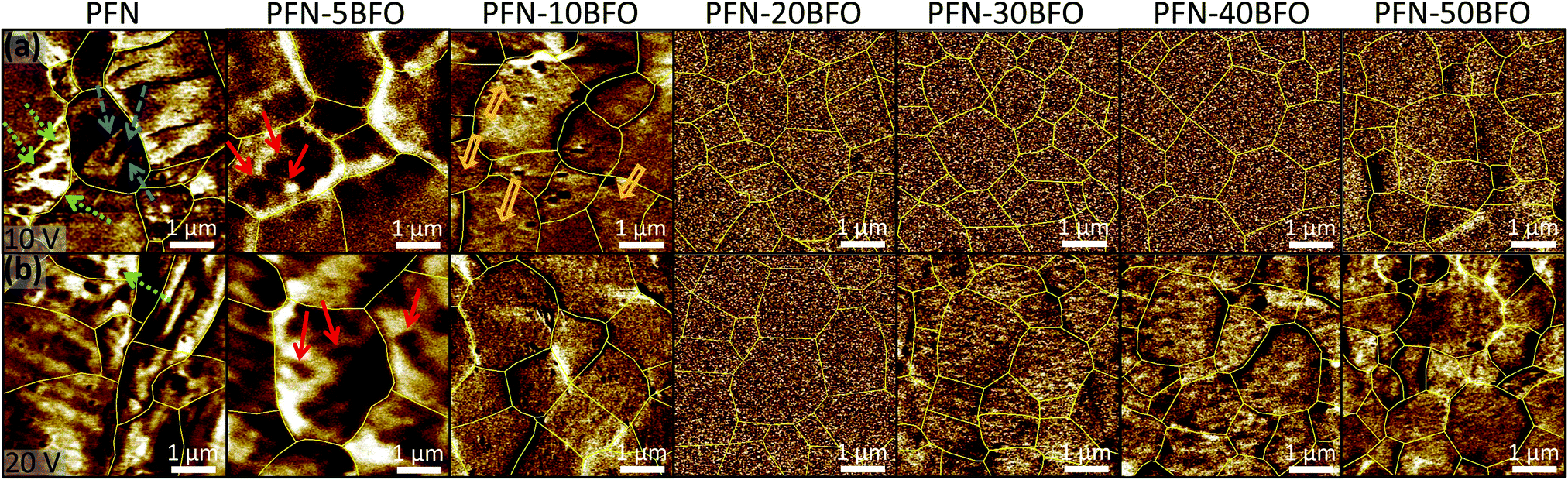 | ||
| Fig. 7 PFM out-of-plane amplitude images obtained by scanning with AC drive signals of (a) 10 V and (b) 20 V of PFN–100xBFO (x = 0–0.5). Sub-micron-sized wedge domains are marked by blue dashed arrows. Irregular sub-micron-sized domains, a few hundred nm-large domains and a few tens of nm-large domains are marked by green dotted, red solid and orange open arrows, respectively. | ||
When samples were scanned at an AC drive amplitude of 20 V (Fig. 7b), the piezo-response signal starts to appear in x ≥ 0.3 compositions. This fine-grain response can be attributed to clusters of piezo-active polar nano-regions that reorganize under applied electric field as previously suggested for Pb-based relaxors.51 These induced regions are several tens of nanometers in size. After 24 h, the same areas were scanned again with an AC drive amplitude of 10 V. During these scans, zero piezo-signal was observed again (similar to the ones in Fig. 7a for x ≥ 0.2) indicating reversible electric field-induced phenomenon.
P–E hysteresis loops of all PFN–100xBFO compositions are shown in Fig. 8. In pure PFN, ferroelectric square-like hysteresis loops were observed,52 which is in agreement with previous reports.11,42,53 The remanent polarization (Pr) and coercive filed (Ec) of pure PFN are ∼22 μC cm−2 and ∼3.5 kV cm−1, respectively. With increasing contents of BFO up to x = 0.2, P–E loops become slimmer and tilted, indicating increased relaxor behavior in agreement with aforementioned analyses. Similar to the P–E loops, the more pronounced relaxor behavior is also reflected in the S–E measurements, which show a more quadratic-like response with diminished hysteresis, characteristic for electrostrictive response (ESI† material, I). This is the first time when P–E loops of PFN–100xBFO (x ≤ 0.5) solid solutions were systematically studied, therefore a comparison with the literature data is not possible.
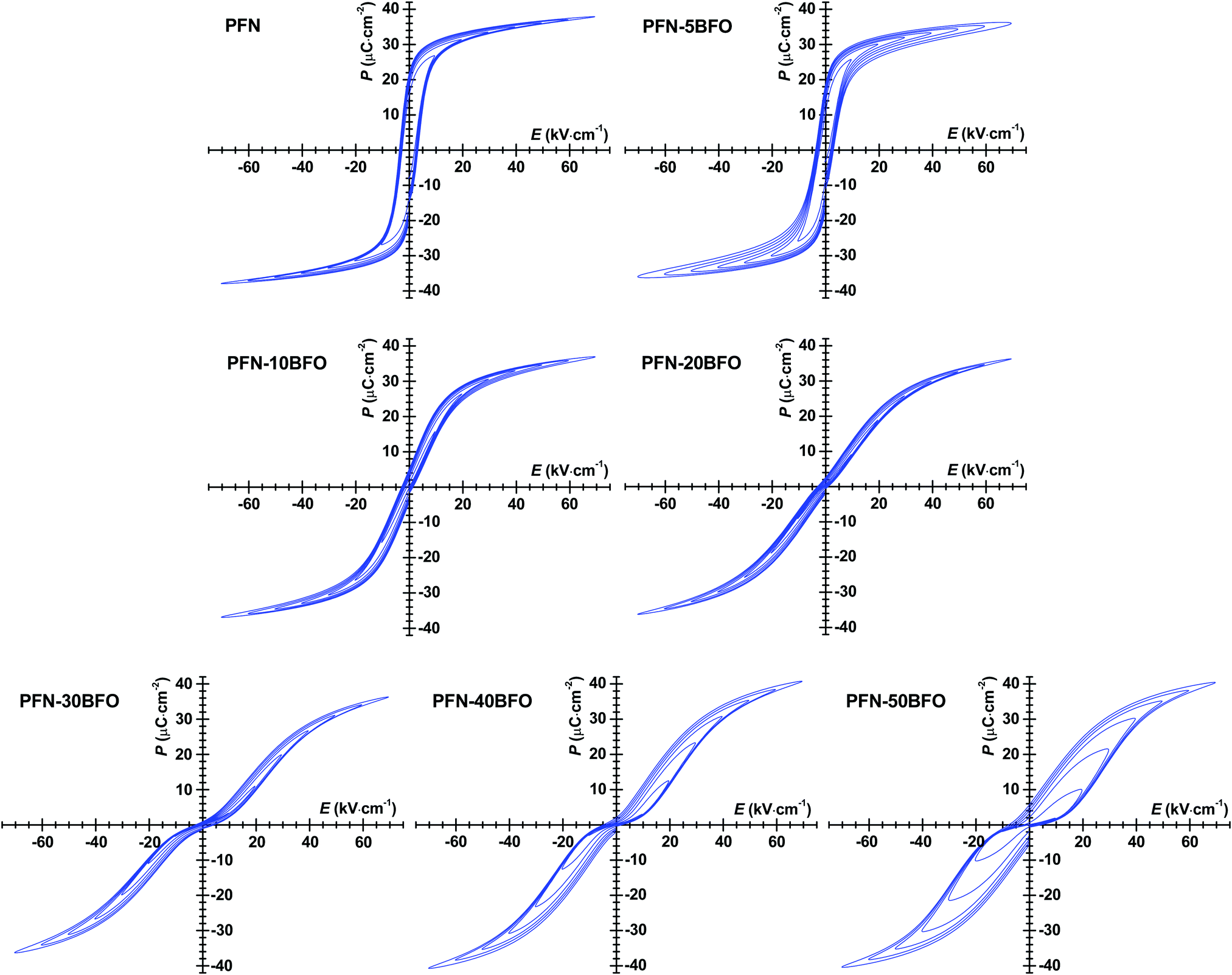 | ||
| Fig. 8 P–E hysteresis loops of PFN–100xBFO (x = 0–0.5) at RT measured with increasing electric-field amplitude at driving frequency of 1 Hz. | ||
In compositions with higher BFO content (x = 0.2–0.5), P–E loops develop a pinched shape and gradually become thicker (show larger hysteresis). Pinching is more evident in the AC current density–electric field (J–E) hysteresis loops by the appearance of double current peaks (ESI† material, J). In general, there can be many reasons for the appearance of pinched P–E loops.52 One reason could be related to the AFE ordering observed in HRTEM study. Due to the antisymmetric crystal sublattices this typically results in a double P–E hysteresis loop.52 Often, pinching can also be related to electric-field-induced relaxor-to-ferroelectric phase transition that occurs during the measurement, as previously reported in Pb(Sc0.5Ta0.5)O354 and Pb(Sc0.5Nb0.5)O355 ceramics. In these two cases, the pinching was related to the coexistence of ferroelectric and relaxor phases and transition between them induced by application of high electric fields. Another reason for the pinched behavior is associated with the presence of charged point defects, such as oxygen vacancies or other type of defects which act as strong pinning centers for domain walls or similar interfaces. As previously demonstrated in Pb(Zr,Ti)O3 ceramics,56–58 an indirect evidence that pinching is indeed related to the pinning behavior of such charged point defects is obtained from a continues AC electric-field-cycling experiments and measurements of P–E and J–E hysteresis loops at different frequencies where the hysteresis loops eventually opens up or relaxes during field cycling. These experiments, provided for our PFN–BFO in ESI† material K, show that cycling of PFN–50BFO sample do not affect the shape of the P–E hysteresis loop, i.e., the loop remains pinched. However, the additional rapid cooling (quenching) experiment shows that P–E hysteresis loops were partially de-pinched; in this experiment the loop is expected to completely depinch if the pinching is controlled by charged point defects because quenching leads to redistribution of the defects from an ordered (pinched) to a disordered (depinched) state (ESI† material, L).59 Therefore, the influence of the charged point defects on pinching in PFN–50BFO cannot be completely excluded, however it appears as defects have still a minor role in the pinching behavior.
In order to further investigate the origin of electric-field induced phenomena, synchrotron X-ray diffraction (sXRD) measurements of PFN–50BFO were employed. Maps of the 111 and 200 pseudocubic reflections during in situ applied voltage up to 50 kV cm−1 and after release are shown in Fig. 9. From the measurements, it seems that PFN–50BFO does not exhibit a classical field-induced phase transition; however, the data contain some interesting features, including broadening and weakening in intensity of all peaks parallel to the field direction. These changes are isotropic and recoverable. Most probably, the transition involves changes at a length scale smaller than visible by diffraction, possibly deformation or reorganization of polar regions at the nanoscale (Fig. 7b) into larger clusters, which transform back when the electric field is removed. Similar behavior was also observed in BiFeO3–BaTiO3 based ceramics,60 but in general, this phenomenon is not yet well described in the literature. In situ sXRD measurements were also performed for PFN–40BFO composition (ESI† material, M). However, the changes in intensity of peaks under the electric field are not so pronounced as in the case of PFN–50BFO, which is consistent with slimmer P–E and S–E hysteresis loops and consequently smaller pinching of PFN–40BFO.
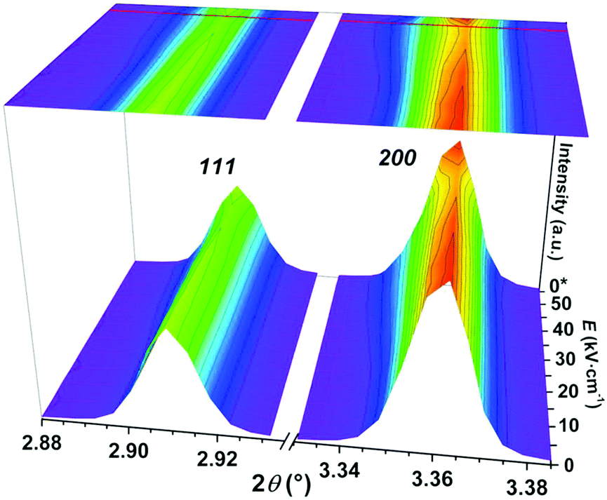 | ||
| Fig. 9 Room-temperature in situ sXRD surface contour plots of the 111 and 200 pseudocubic reflections of PFN–50BFO with in situ applied voltage up to 50 kV cm−1 and after release (*0 kV cm−1). | ||
The strengthening of the relaxor features in PFN–100xBFO solid solution is also reflected in piezoelectric properties. The values of piezoelectric coefficient d33 of all studied compositions are shown in Fig. 10. The measurements were performed 24 h after poling so that any reversible electric-filed-induced changes that are observed in measurements under in situ applied electric field (see above sXRD and PFM measurements) are already relaxed back to the initial state. PFN exhibits the highest d33 of ∼145 pC N−1, which is consistent with previously reported values.5,10d33 of PFN–100xBFO solid solutions gradually decreases with increasing BFO content and drops to almost zero in x ≥ 0.2 compositions as expected for relaxor systems.
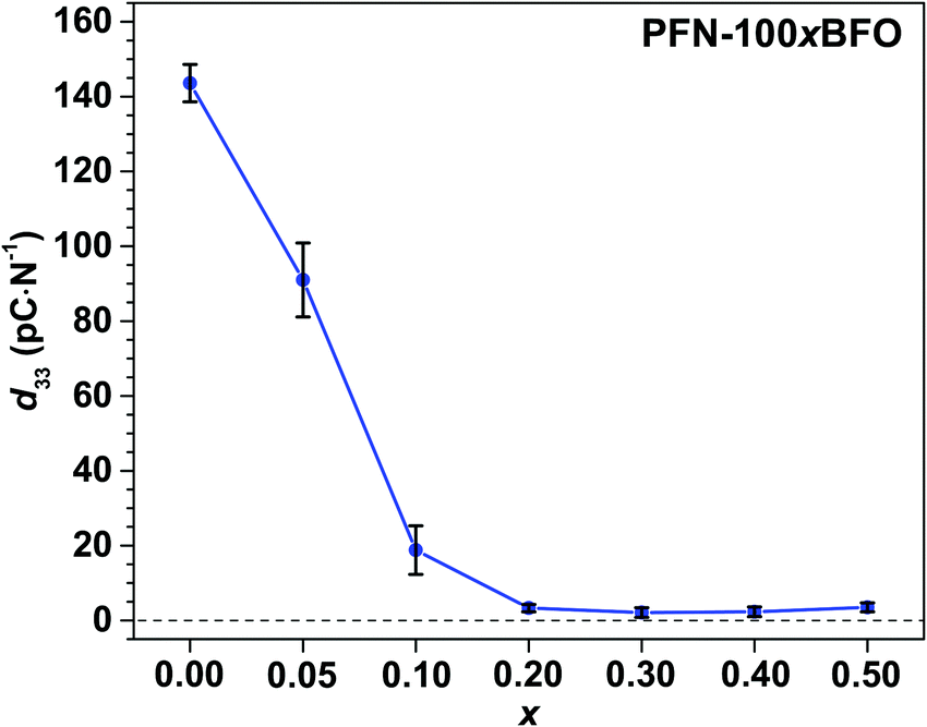 | ||
| Fig. 10 Piezoelectric coefficient d33 of PFN–100xBFO (x = 0–0.5). | ||
IV. Summary and conclusions
In this work, PFN–100xBFO (x = 0, 0.05, 0.1, 0.2, 0.3, 0.4 and 0.5) solid solutions were successfully prepared by mechanochemical synthesis followed by sintering at different temperatures. An optimized processing procedure resulted in the preparation of highly dense single-phase ceramics with comparable grain size and relatively low dielectric losses, which enable the systematic study of dielectric, ferroelectric and electromechanical properties of the PFN–BFO solid solutions.PFN crystalizes in monoclinic symmetry. It exhibits well-defined and open P–E hysteresis loops with remanent polarization and coercive field values of ∼22 μC cm−2 and ∼3.5 kV cm−1, respectively. Sub-micrometer-sized ferroelectric domains were observed by PFM and TEM. Introducing BFO into the PFN–BFO solid solution leads to the formation of a pseudocubic phase and consequently to enhanced relaxor-like behavior obeying the Vogel–Fulcher law.
The PFN–BFO compositions with small amounts of BFO (x = 0.05 and 0.1) exhibit coexistence of monoclinic and pseudocubic phases, which are accompanied by a broadening of dielectric peak-permittivity, slimmer P–E hysteresis loops, sub-micrometer irregularly shaped ferroelectric domains and a gradual decrease in the piezoelectric response compared to pure PFN. When adding extra BFO into the structure (x = 0.2–0.5), only pseudocubic symmetry is present. In these compositions, nanometer sized domains are observed by TEM. Additionally, superlattice ½ ½ 0 reflections are observed in PFN–50BFO form the HRTEM analysis, but not detected by XRD. These superlattice reflection indicate that anti-ferroelectric nanoislands are embedded in the pseudocubic relaxor phase.
During high-field electric properties measurements, recoverable electric-field phenomena appears, which is reflected in pinching of the P–E hysteresis loops. This is most probably related to several factors such as the reorganization of polar nano-domains into clusters under the electric field, AFE order and charged point defects present in the material.
In conclusion, PFN–10BFO and PFN-20BFO exhibit slim P–E hysteresis loops and peak-permittivity temperatures near ambient temperature, which make them promising for electrocaloric cooling applications. On the other hand, low hysteresis losses and electrostriction of PFN–20BFO and PFN–30BFO make these materials also potentially useful for energy storage applications and precision displacement actuators.
Conflicts of interest
There are no conflicts to declare.Acknowledgements
The authors thank the financial support from the Slovenian Research Agency (project Multicaloric cooling J2-9253, young researcher project PR-07594, bilateral project BI-US/19-21-062 and research core funding No. P2-0105). Technical support by Brigita Kmet (from JSI), Milan Baricevic and Marko Mudri (Erasmus+ programme) is gratefully acknowledged. Centre of Excellence NAMASTE is acknowledged for access to the AFM equipment. This research used resources of the Advanced Photon Source, a U.S. Department of Energy (DOE) Office of Science User Facility operated for the DOE Office of Science by Argonne National Laboratory under Contract No. DE-AC02-06CH11357. Contributions from RS and GB were supported by a CoorsTek Fellowship and the US National Science Foundation (DMR-1555015), respectively.References
- G. Catalan and J. F. Scott, Adv. Mater., 2009, 21, 2463–2485 CrossRef CAS.
- T. Rojac, A. Bencan, B. Malic, G. Tutuncu, J. L. Jones, J. E. Daniels and D. Damjanovic, J. Am. Ceram. Soc., 2014, 97, 1993–2011 CrossRef CAS.
- V. A. Bokov, I. E. Mylnikova and G. A. Smolenskii, J. Exp. Theor. Phys., 1962, 42, 643–646 CAS.
- C. C. Chiu and S. B. Desu, Mater. Sci. Eng., B, 1993, 21, 26–35 CrossRef.
- M. Yokosuka, Jpn. J. Appl. Phys., 1993, 32, 1142–1146 CrossRef CAS.
- R. Havlicek, J. Poltierova Vejpravova and D. Bochenek, J. Phys.: Conf. Ser., 2010, 200, 012058 CrossRef.
- O. Raymond, R. Font, N. Suarez-Almondovar, J. Portelles and J. M. Siqueiros, J. Appl. Phys., 2005, 97, 084108 CrossRef.
- S.-B. Lee, S.-H. Yoon and H. Kim, J. Eur. Ceram. Soc., 2004, 24, 2465–2470 CrossRef CAS.
- C. Stock, S. R. Dunsiger, R. A. Mole, X. Li and H. Luo, Phys. Rev. B: Condens. Matter Mater. Phys., 2013, 88, 094105 CrossRef.
- H. Ursic, A. Bencan, U. Prah, M. Dragomir and B. Malic, Materials, 2019, 12, 1327 CrossRef CAS.
- U. Prah, T. Rojac, M. Wencka, M. Dragomir, A. Bradesko, A. Bencan, R. Sherbondy, G. Brennecka, Z. Kutnjak, B. Malic and H. Ursic, J. Eur. Ceram. Soc., 2019, 39, 4122–4130 CrossRef CAS.
- R. Mackeviciute, V. Goian, S. Greicius, R. Grigalaitis, D. Nuzhnyy, J. Holc, J. Banys and S. Kamba, J. Appl. Phys., 2015, 117, 084101 CrossRef.
- T. Rojac, M. Makarovic, J. Walker, H. Ursic, D. Damjanovic and T. Kos, Appl. Phys. Lett., 2016, 109, 042904 CrossRef.
- C. F. Buhrer, J. Chem. Phys., 1962, 36, 798–803 CrossRef CAS.
- G. A. Smolenskii and V. M. Yudin, Phys. Solid State, 1965, 6, 2936–2942 Search PubMed.
- N. N. Krainik, N. P. Khuchua, A. A. Berezhnoi and A. G. Tutov, Phys. Solid State, 1965, 7, 100–107 Search PubMed.
- V. V. Zhdanova, Phys. Solid State, 1965, 7, 108–111 Search PubMed.
- I. H. Ismailzade, R. M. Ismailov, A. I. Alekperov and F. M. Salaev, Phys. Status Solidi A, 1980, 57, 99–103 CrossRef CAS.
- I. O. Troyanchuk, M. V. Bushinsky, A. N. Chobot, O. S. Mantytskaya, N. V. Pushkarev and R. Szymczak, J. Exp. Theor. Phys., 2008, 107, 245–250 CrossRef CAS.
- D. Bochenek, R. Zachariasz, J. Ilczuk and J. Dudek, Acta Phys. Pol., A, 2009, 116, 274–276 CrossRef CAS.
- J. P. Patel, A. Singh and D. Pandey, J. Appl. Phys., 2010, 107, 104115 CrossRef.
- L. A. Shilkina, A. V. Pavlenko, L. A. Reznitchenko and I. A. Verbenko, Crystallogr. Rep., 2016, 61, 263–269 CrossRef CAS.
- A. Stoch, J. Maurin, J. Kulawik and P. Stoch, J. Eur. Ceram. Soc., 2017, 37, 1467–1476 CrossRef CAS.
- D. Bochenek, P. Niemiec, P. Guzdek and M. Wzorek, Mater. Chem. Phys., 2017, 195, 199–206 CrossRef CAS.
- A. Stoch and P. Stoch, Ceram. Int., 2018, 44, 14136–14144 CrossRef CAS.
- F. Li, S. Zhang, D. Damjanovic, L.-Q. Chen and T. R. Shrout, Adv. Funct. Mater., 2018, 28, 1801504 CrossRef.
- D. Damjanovic and R. E. Newnham, J. Intell. Mater. Syst. Struct., 1992, 3, 190–208 CrossRef.
- M. Vrabelj, H. Ursic, Z. Kutnjak, B. Rozic, S. Drnovsek, A. Bencan, V. Bobnar, L. Fulanovic and B. Malic, J. Eur. Ceram. Soc., 2016, 36, 75–80 CrossRef CAS.
- T. Rojac and M. Kosec, in High-Energy Ball Milling, ed. M. Sopicka-Lizer, Woodhead Publishing, 1st edn, 2010, ch. 6, pp. 113–148 Search PubMed.
- H. Ursic, A. Bencan, G. Drazic, G. Esteves, J. L. Jones, T.-M. Usher, T. Rojac, S. Drnovsek, M. Deluca, J. Jouin, V. Bobnar, G. Trefalt, J. Holc and B. Malic, J. Mater. Chem. C, 2015, 3, 10309–10315 RSC.
- R. Jimenez, H. Amorin, J. Ricote, J. Carreaud, J. M. Kiat, B. Dkhil, J. Holc, M. Kosec and M. Alguero, Phys. Rev. B: Condens. Matter Mater. Phys., 2008, 78, 094103 CrossRef.
- Y. Tan, J. Zhang, Y. Wu, C. Wang, V. Koval, B. Shi, H. Ye, R. McKinnon, G. Viola and H. Yan, Sci. Rep., 2015, 5(9953), 1–9 Search PubMed.
- R. Font, O. Raymond-Herrera, L. Mestres, J. Portelles, J. Fuentes and J. M. Siqueiros, J. Mater. Sci., 2016, 51, 6319–6330 CrossRef CAS.
- D. Pfoertsch and C. Ruud, Penn State University, University Park, Pennsylvania, USA, ICDD Grant-in-Aid, PDF No. 032-0522, 1981.
- R. W. Cheary and A. Coelho, J. Appl. Crystallogr., 1992, 25, 109–121 CrossRef CAS.
- D. Wilcox, B. Dove, B. McDavid and D. Greer, UTHSCSA Image Tool for Windows Version 3.0, University of Texas Health Science Center, San Antonio, TX, 2002 Search PubMed.
- W. H. Walton, Nature, 1948, 162, 329–330 CrossRef.
- D. B. Williams and C. B. Carter, Transmission Electron Microscopy, A Textbook for Materials Science, Springer, Boston, MA, USA, 2009 Search PubMed.
- N. Lampis, P. Sciau and A. G. Lehmann, J. Phys.: Condens. Matter, 1999, 11, 3489–3500 CrossRef CAS.
- I.-K. Jeong, J. S. Ahn, B. G. Kim, S. Yoon, S. Pal Singh and D. Pandey, Phys. Rev. B: Condens. Matter Mater. Phys., 2011, 83, 064108 CrossRef.
- S. Ananta and N. W. Thomas, J. Eur. Ceram. Soc., 1999, 19, 2917–2930 CrossRef CAS.
- R. Font, O. Raymond, E. Martinez, J. Portelles and J. M. Siqueiros, J. Appl. Phys., 2009, 105, 114110 CrossRef.
- I. Grinberg, P. Juhas, P. K. Davies and A. M. Rappe, Phys. Rev. Lett., 2007, 99, 267603 CrossRef PubMed.
- R. Pirc and R. Blinc, Phys. Rev. B: Condens. Matter Mater. Phys., 2007, 76, 020101 CrossRef.
- H. Ursic and D. Damjanovic, Appl. Phys. Lett., 2013, 103, 072907 CrossRef.
- H. Vogel, Phys. Z., 1921, 22, 645 CAS.
- G. S. Fulcher, J. Am. Ceram. Soc., 1925, 8, 339–355 CrossRef CAS.
- A. A. Bokov and Z. G. Ye, J. Mater. Sci., 2006, 41, 31–52 CrossRef CAS.
- A. M. Glazer, Acta Crystallogr., Sect. A: Found. Crystallogr., 1975, 31, 756–762 CrossRef.
- A. Tkachuk and H. Chen, AIP Conf. Proc., 2003, 677, 55–64 CrossRef CAS.
- V. V. Shvartsman, A. L. Kholkin, A. Orlova, D. Kiselev, A. A. Bogomolov and A. Sternberg, Appl. Phys. Lett., 2005, 86, 202907 CrossRef.
- T. Schenk, E. Yurchuk, S. Mueller, U. Schroeder, S. Starschich, U. Böttger and T. Mikolajick, Appl. Phys. Rev., 2014, 1, 041103 Search PubMed.
- B. Fraygola, N. Frizon, W. J. Nascimento, A. A. Coelho, D. Garcia and J. A. Eiras, Ferroelectrics, 2014, 470, 221–226 CrossRef CAS.
- F. Chu, N. Setter and A. K. Tagantsev, J. Appl. Phys., 1993, 74, 5129–5134 CrossRef CAS.
- F. Chu, I. M. Reaney and N. Setter, J. Appl. Phys., 1995, 77, 1671–1676 CrossRef CAS.
- M. I. Morozov and D. Damjanovic, J. Appl. Phys., 2008, 104, 034107 CrossRef.
- T. Rojac, S. Drnovsek, A. Bencan, B. Malic and D. Damjanovic, Phys. Rev. B, 2016, 93, 014102 CrossRef.
- K. Carl and K. H. Hardtl, Ferroelectrics, 1978, 17, 473–486 CrossRef CAS.
- D. Damjanovic, in The Science of Hysteresis, ed. I. Mayergoyz and G. Bertotti, Elsevier, vol. 3, 2006, ch. 4, pp. 337–465 Search PubMed.
- G. Wang, Z. Fan, S. Murakami, Z. Lu, D. A. Hall, D. C. Sinclair, A. Feteira, X. Tan, J. L. Jones, A. K. Kleppe, D. Wang and I. M. Reaney, J. Mater. Chem. A, 2019, 7, 21254–21263 RSC.
Footnote |
| † Electronic supplementary information (ESI) available. See DOI: 10.1039/c9tc05883d |
| This journal is © The Royal Society of Chemistry 2020 |