
A few-layer InSe-based sensitivity-enhanced photothermal fiber sensor
Rui
Wang†
ab,
Qing
Wu†
c,
Xiantao
Jiang
a,
Taojian
Fan
 a,
Jia
Guo
a,
Cong
Wang
a,
Feng
Zhang
a,
Yali
Gao
b,
Meng
Zhang
*c,
Zhengqian
Luo
*b and
Han
Zhang
*a
a,
Jia
Guo
a,
Cong
Wang
a,
Feng
Zhang
a,
Yali
Gao
b,
Meng
Zhang
*c,
Zhengqian
Luo
*b and
Han
Zhang
*a
aCollaborative Innovation Center for Optoelectronic Science & Technology, International Collaborative Laboratory of 2D Materials for Optoelectronics Science and Technology of Ministry of Education, Guangdong Laboratory of Artificial Intelligence and Digital Economy (SZ), College of Optoelectronic Engineering, Shenzhen University, Shenzhen 518060, China. E-mail: hzhang@szu.edu.cn
bDepartment of Electronic Engineering, Xiamen University, Xiamen 361005, P. R. China. E-mail: zqluo@xmu.edu.cn
cSchool of Electronic and Information Engineering, Beihang University, Beijing, 100191, P. R. China. E-mail: mengzhang10@buaa.edu.cn
First published on 13th November 2019
Abstract
Two-dimensional (2D) InSe has recently attracted increasing attention due to its outstanding electrical transport property, excellent photo-response, and direct band gap characteristics. In this contribution, few-layer InSe was successfully fabricated via a facile liquid phase exfoliation (LPE) method. Compared with other 2D materials, the photothermal response measurements demonstrate that InSe has excellent photothermal conversion efficacy. A novel Vernier-cascaded photothermal fiber sensor with high sensitivity that takes advantage of the photothermal effect of few-layer InSe has been proposed and demonstrated for the first time. The experimental results have shown that the photothermal optical sensitivity and spectral shifts of the MZI (Mach–Zehnder interferometer)–MKR (microfiber knot ring) Vernier sensor and the Vernier part are 0.126 nm mW−1, 12.22 nm and 0.0047 nm mW−1, 0.49 nm, respectively. A maximum sensitivity amplification factor of ∼26.8 is realized. Our present work can provide more possibilities of 2D materials that can be utilized towards cascade sensors.
Introduction
Since the ground-breaking discovery of graphene in 2004,1 the research in two-dimensional (2D) materials has made a series of progresses in the fields of photovoltaic devices,2,3 catalysis,4,5 and energy storage applications.6,7 One of the most impressive advantages of 2D materials is their high surface-to-volume ratio, which can be translated into highly sensitive sensor applications.8–11 Recently, the compound semiconductor indium selenide (InSe) from the III–VI group has been attracting considerable attention due to its outstanding electronic and optical properties.12 As a promising binary semiconductor compound, InSe features a 2D hexagonal lattice in the atomic plane and each layer has four atomic planes connected by a covalent bond (Se–In–In–Se). Moreover, InSe presents broad absorption in the UV-Vis-NIR absorption region. Moreover, compared with other 2D materials, the photothermal response measurements demonstrate that InSe has excellent photothermal conversion efficacy and the previous reports also illustrate that InSe possesses high thermal stability up to 660 °C.13 Due to the ascendant properties of InSe including the broad absorption, high surface-to-volume ratio, excellent photothermal conversion efficacy and thermal stability, direct bandgap for easy light coupling, the fabrication of InSe-based photothermal fiber sensors has attracted considerable interest.Currently, optical fiber sensors based on cascade interferometers have been reported in the fields of physical sciences, chemical sciences, biology, and environment.14–16 Fiber optic sensors can be classified into two categories based on the different roles played by the fiber in the system: (1) the physical fiber sensor (sensing fiber-optic sensors) is sensitive to environmental changes. Sensing fiber-optic sensors typically require special fibers and are costly. On the other hand, cascaded sensing fiber-optic sensors require one of two interferometers to be sensitive enough to measure physical quantities and the other to be insensitive. (2) A structured optical fiber sensor (light-transmitting fiber-optic sensors) is a measurement system in which an optical fiber serves only as a propagation medium for light. Among them, a single-mode optical fiber is often used and the external signal is modulated by the external modulation device to the optical wave entering the optical fiber. The advantages are that the fiber can be used for data transmission and the signal is immune to electromagnetic interference.
The Vernier effect is often used in structured optical fiber sensors. Vernier calipers and barometers first used the Vernier effect to improve the accuracy of length and barometric measurements. Recently, the Vernier effect has also been used for fiber sensing to amplify spectral shifts. The use of two interferometers to achieve the Vernier effect has been extensively applied to fiber optic sensors.17–20 In the past few years, the Vernier effect has been widely used to improve the accuracy and sensitivity of measuring instruments.20–24 Representative fiber optic interferometers comprise four types: Fabry–Perot interferometer (FPI), Mach–Zehnder interferometer (MZI), Michelson interferometer (MI), and Sagnac interferometer (SI). Two interferometers are used as the sensing part and the reference part, respectively.25–33 When the interferometer is modulated by an external sensing signal, the Vernier interference fringes will drift, and the amount of fringe movement far exceeds the drift of the interferometer's own spectral fringes, which is the basis for achieving high sensitivity sensing. The Vernier interference fringes have a delicate structure; however, the sensing signal is modulated onto the fringe envelope. Therefore, when performing spectral demodulation, the spectral envelope is simply measured by a spectrometer. As we know, waveguides, high non-linear fibers, fiber grating, and in-line MZIs have all been applied to sensors but all of them have the disadvantages of high cost and poor adjustability. In-line MZIs have large loss and mode interference, which lead to messy spectra.
In this manuscript, a novel and economical cascaded photothermal fiber sensor based on the photothermal effect of 2D materials was constructed for the first time. The few-layer InSe with high photothermal conversion efficiency was deposited onto the surface of the microfiber by an optical deposition method. Under irradiation of 980 nm pump light, few-layer InSe generates heat and changes the refractive index of the fiber, thus adjusting the spectral shift of the interferometer. The measurement parameters of the MZI–MKR Vernier photothermal fiber sensor based on the cursor effect designed in this paper are modularized. When the light power is 108 mW, the spectral shift in a single sensing interferometer is 0.49 nm and the spectral envelope shift in the Vernier interference fringes is measured as 12.22 nm. The photothermal optical sensitivity of a single sensor interferometer and cascaded interferometer are 0.0047 nm mW−1 and 0.126 nm mW−1, respectively. Thus, the sensitivity is magnified by 26.8 times, which is consistent with the theoretical value. In addition, considering the superior stability of MKR and photothermal conversion efficiency of InSe, we believe that these findings give an insight into the photothermal fiber sensor and the proposed InSe-based sensitivity-enhanced photothermal fiber sensor possesses great potential for use in optical imaging, chemical, and biomedical research.
Fabrication and morphology characterization
Bulk InSe crystal (99.99%) was purchased from Nanjing MKNANO Tech. Co., Ltd. N-Methyl-2-pyrrolidone (NMP, 99.5%) was purchased from Aladdin Co., Inc. A typical liquid-phase exfoliation (LPE) method was employed to fabricate few-layer InSe.12,34 Briefly, the few-layer InSe was prepared by probe sonication and bath sonication with the assistance of centrifugation.35 100 mg bulk InSe crystal was grinded into powder with 100 mL NMP for 4 h. After grinding, the InSe–NMP suspension with concentration of 1 mg mL−1 was probe sonicated for 12 hours, which can provide enough energy to exfoliate bulk InSe into few-layer InSe effectively. Then, further bath sonication was employed with a power of 400 W for 72 hours. During these processes, the van der Waals interactions between the layers of bulk InSe could easily break and the liquid environment of NMP could further expand the interspace of the molecular layers.36 The few-layer InSe can be obtained ultimately by extracting the supernatant in the obtained InSe/NMP suspension after centrifugation at 3000 rounds per minute (rpm) for 3 min.UV-Vis-NIR absorption spectra of NMP solvent (black line) and few-layer InSe in NMP solvent (red line) were recorded in the spectral range of 300–1200 nm, as shown in Fig. 1a. The obtained few-layer InSe (Fig. 1a left insert) can be well dispersed in NMP (Fig. 1a right insert) without any visible precipitation at room temperature for more than three days. Contrary to the nearly zero absorbance of NMP solvent, few-layer InSe presents wide absorption characteristics in all of the measured spectral range and as the wavelength increases, the absorbance gradually decreases. This broadband absorption range implies that few-layer InSe has potential applications in UV-NIR devices. In addition, we plotted α2versus hν to determine the energy band gap of few-layer InSe (Fig. 1a inset), where α is the linear absorption coefficient and h is the photon energy.2,37 The calculated energy band gap is 1.95 eV, which is well in agreement with the earlier reports.35,38,39 We used the Raman microscope (HORIBA Lab RAM Xplora) to investigate the structure and vibrational modes of the few-layer InSe at room temperature with the excitation wavelength of 532 nm and the measurement result is shown in Fig. 1b. There are four active resonant Raman modes at A1 (114 cm−1), E (175 cm−1), A1(LO) (198 cm−1), and A1 (225 cm−1) that can be observed from 100 to 300 cm−1, which are consistent with the previous reports.40 Transmission electron microscopy (TEM, Tecnai G2 Spirit 120 kV) measurement of the few-layer InSe was performed and the result is displayed in Fig. 1c. It is easy to see that few-layer InSe was exfoliated with a horizontal size ranging from 80 nm to 240 nm. The topographic morphology of few-layer InSe was studied by employing atomic force microscopy (AFM, Bruker) (Fig. 1d). In this experiment, the heights of the few-layer InSe can be precisely evaluated. The measured heights (yellow lines) and corresponding statistical analysis of few-layer InSe are shown in Fig. 1d. The statistical values of the heights of few-layer InSe are 7.7 nm (∼9 L), 9.2 nm (∼11 L), 11.5 nm (∼14 L), and 5.4 nm (∼6 L). These statistical heights confirm that we successfully and efficiently prepared few-layer InSe by LPE. High-resolution TEM (HRTEM) image (Fig. 1f) clearly presents the crystal lattice spacing of ∼0.341 nm, which can be well assigned to the (101) plane of InSe. In addition, the corresponding selected area electron diffraction (SAED) image (Fig. 1f inset) presents a 6-fold symmetry feature that also demonstrates the high crystal quality of the as-prepared few-layer InSe.41
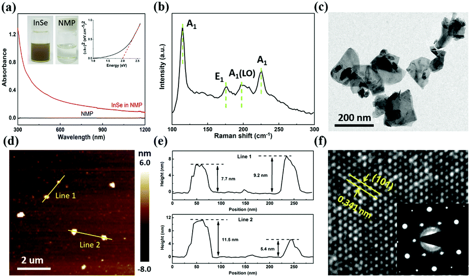 | ||
| Fig. 1 Characterization of the few-layer InSe: (a) UV-Vis-NIR absorption spectra of NMP solvent (black line) and few-layer InSe in NMP solvent (red line). Left inset: Photos of the few-layer InSe and NMP solvent. Right inset: The calculated energy band gap of the few-layer InSe. (b) Raman spectra of the few-layer InSe. (c) TEM image illustrates the size of the few-layer InSe. (d) AFM image of the as-prepared few-layer InSe. (e) Height profiles along the yellow lines in (c). (f) HRTEM image of the few-layer InSe and the measured lattice fringe is 0.341 nm. The inset shows the SAED image. | ||
Photothermal response
Recently, a series of progresses has been made based on the thermo-optical effect of 2D materials in the field of biology and communication.42–44 However, there are few reports about the application of 2D materials for thermo-optical effect in photothermal fiber sensors. Therefore, to explore the potential of 2D materials being utilized for photothermal fiber sensor, the photothermal properties of the few-layer InSe were further evaluated.We dispersed few-layer InSe into 1 mL deionized water and placed them into quartz cuvette with a diameter of 10 mm. Then, we used a 980 nm laser diode to irradiate the samples and a thermal detector to record changes in the temperature of the samples with the frequency of 1 Hz. Subsequently, the time-dependent temperature changes in the as-prepared 1 mg mL−1 few-layer InSe dispersed in deionized water under irradiation were recorded, as shown in Fig. 2a. During the heating period (108 mW), the temperature increased significantly from 22.6 to 26.2 °C, indicating that the few-layer InSe can efficiently convert NIR light (980 nm) into thermal energy. Then, the temperature changed dramatically after turning off the laser. Moreover, by using a previously reported method, the photothermal conversion efficacy of few-layer InSe was determined to be 43.6% (Fig. 2b), which is higher than a series of photothermal nanomaterials, such as Au nanoparticles (21%),45,46 black phosphorus quantum dots (28.4%),47 graphene oxide (25%),48 and SnS nanosheets (39.3%)42 but lower than that of MoS2 (53.3%).49 In addition, we further studied the photothermal response of deionized water to exclude the effects of water in few-layer InSe. It is easily to see (Fig. 2c) that the change in the temperature is significantly reduced under irradiation with 108 mW, indicating the weak photothermal effect of deionized water. On the other hand, the change in temperature sharply increases after increasing the incident power to 600 mW, demonstrating the ability to measure high power of the few-layer InSe-based device. Besides, the flatness of the dotted lines shows the stability of photothermal response, indicating that few-layer InSe has potential as a photothermal device in fiber-optic sensors.
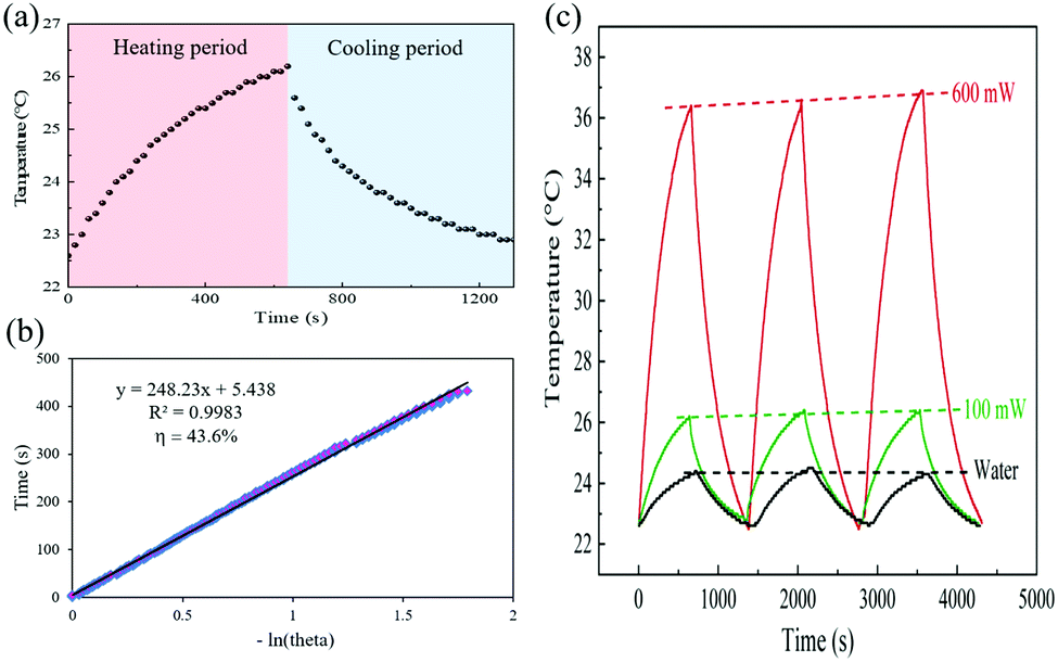 | ||
| Fig. 2 Photothermal conversion efficacy measurements: (a) the photothermal heating curve (red region) of the few-layer InSe under irradiation (108 mW) and the cooling curve (blue region) after turning off the laser. (b) Linear fitting between -ln(theta) and time obtained from the cooling period of (a). (c) Photothermal heating and cooling curves of deionized water and few-layer InSe dispersed in deionized water under irradiation of 108 mW and 600 mW with a 980 nm laser for three cycles. The dotted lines show the stability of photothermal response. | ||
Experiments and discussions
As shown in Fig. 3, the photothermal fiber sensor consisted of MZI, MKR, and few-layer InSe-based device. A microfiber was prepared using the flame drawing method and a few-layer InSe-based device was prepared by optical deposition. The InSe-deposited microfiber was inserted into one arm of the MZI. The preparation of MKR is dependent on the basis of the microfiber. An optical source (ASE OS8143) with a wavelength range of 1526–1566 nm is used as the input source. The reference MKR with a stable diameter as the main part of the Vernier-scale while the sensing MZI based on the material device is used as the Vernier part of the Vernier-scale due to the adjustable lengths of the two interference arms. The sensing MZI interferometer used motorized variable optical delay line (GPC-MDL-002) to adjust the optical path difference between the two arms. The few-layer InSe deposited onto the microfibers was inserted into one arm of the sensing MZI as the key device. Two 5![[thin space (1/6-em)]](https://www.rsc.org/images/entities/char_2009.gif) :5 optical couplers (OCs) were chosen as the MZI combiner and beam splitter. When the pump light is incident on the few-layer InSe-based device, the material absorbs the pump light to generate heat that changes the refractive index to achieve phase shift of the sensing MZI. The ASE light passes through the cascade configuration and is received by the optical spectral analyzer (Yokogawa AQ6375B) with a resolution of 0.05 nm.
:5 optical couplers (OCs) were chosen as the MZI combiner and beam splitter. When the pump light is incident on the few-layer InSe-based device, the material absorbs the pump light to generate heat that changes the refractive index to achieve phase shift of the sensing MZI. The ASE light passes through the cascade configuration and is received by the optical spectral analyzer (Yokogawa AQ6375B) with a resolution of 0.05 nm.
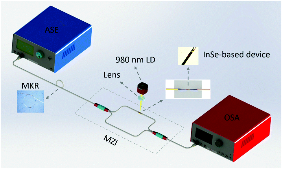 | ||
| Fig. 3 Schematic of a photothermal fiber sensor based on the cascaded configuration of MZI–MKR. | ||
The free spectral range (FSR) of the two interferometers can be used as the main scale and auxiliary scale of the Vernier effect. The Vernier effect is a common mathematical principle that is widely used in the measurement field. The basic principle of optical Vernier effect is similar to that of Vernier caliper measurement. Since the optical Vernier effect is generated by cascading of two interferometers, the optical sensor sensitization mechanism based on optical Vernier effect belongs to the interference sensing mechanism. When the transmission peaks of the two interferometers are aligned, the maximum transmittance can be achieved. Therefore, the cascading transmission spectral envelope is also periodic and the FSRenvelope is related to the FSR of the two interferometers. The FSRR of the MKR is only determined by the diameter of the ring. FSRR = λ2/(2πR·neff), where λ is the incident wavelength, R is the radius of the MKR, and neff is the effective refractive index. It is defined as reference MKR and plays the role of the main scale of the Vernier effect. The other interferometer is defined as sensing MZI. Unlike the MKR, a few-layer InSe-based device was inserted into one of the arms. FSRs = λ2/(L·neff), where L is the length difference between the two arms. FSRR and FSRs are used to represent the FSR of the reference and sensing part. When there is a slight drift in the spectrum of sensing MZI, the position at which the transmission peaks are aligned will change greatly and the period of the corresponding output spectral envelope will also change. According to Vernier effect, the FSR of the envelope and the sensitivity enhancement factor K can be expressed as:

An important note of the Vernier effect is that the main scale is insensitive to the measured parameters but the auxiliary scale is exactly the opposite.
As shown in Fig. 4a, the value of FSRR is 0.3 nm (yellow curve) and the value of FSRs is 0.35 (blue curve). The experimental measurement of FSRenvelope is 2.11 nm (Fig. 4b), which is consistent with the theoretical calculation of 2.10 nm. The enhancement factor K is 6. The interference peaks of FSRR and FSRs partially overlap and the height of each of these peaks will be determined by the amount of overlap. The highest peak of the total output occurs when the peaks of reference MKR and sensing MZI are at the same wavelength of 1546.06 nm.
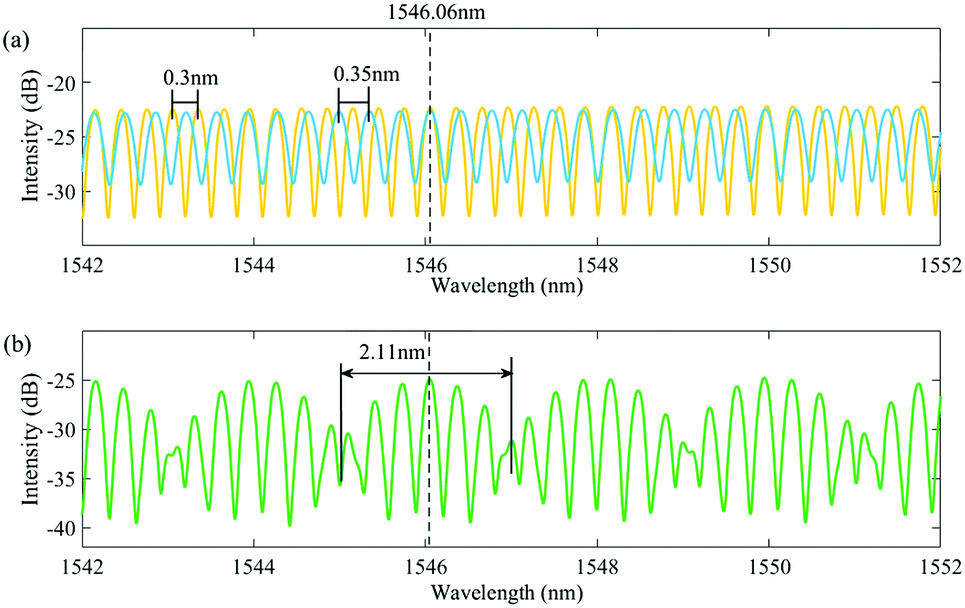 | ||
| Fig. 4 Spectra of (a) reference MKR (yellow) and sensing MZI (blue) (b) cascaded configuration. | ||
From the above analysis, the closer the values of FSRR and FSRs, the higher the sensitivity of the sensor. In addition, the sensing MZI generates a spectral drift based on the photothermal effect of few-layer InSe, which does not affect the reference MKR at all.
In this work, microfibers were fabricated by stretching 1550 nm single-mode fibers directly by hydrogen–oxygen flame method. The obtained microfibers have a loss of less than 5% and the diameter is ∼6–10 μm. The 980 nm light with the power of 40 mW propagation is first through the isolator and then through the microfiber with the diameter of ∼6 μm with a power meter monitoring the output power of the microfiber in real time. The taper region of the microfiber was found under a microscope and the few-layer InSe was dropped in this area using a pipetting gun. The optical microscopic image of the InSe-deposited microfiber with the deposited length of ∼600 μm is illustrated in the inset of Fig. 3. The loss of InSe-deposited microfiber was ∼3 dB measured around 1550 nm and ∼5 dB around 980 nm. It is necessary to fabricate a microfiber having a diameter of about 3 μm and knot it into a ring with a diameter of 1091 μm (see inset of Fig. 3). The MKR diameter we prepared was consistent with that reported previously (0.3–1 mm).50,51 The insertion loss of the MKR is ∼2.7 dB at 980 nm.
Firstly, the transmission spectrum of MKR was tested and the FSRR was 0.47 nm. The theoretical diameter of MKR is 1099 μm, which corresponds to the actual value of 1091 μm. Secondly, the delay line of the sensing MZI was adjusted so that the sensing MZI FSRS was close to the value of FSRR. Fig. 5 shows the spectra of single sensing MZI, reference MKR, and the cascaded structure (pump power = 0 mW). Finally, by adjusting the arm length of MZI, the FSRS close to the FSRR was 0.45 nm. In our experiment, FSRenvelope was 10.13 nm (as shown in Fig. 5c), which is consistent with the theoretical analysis. The calculated theoretical value of the sensitivity enhancement factor K is 23.5.
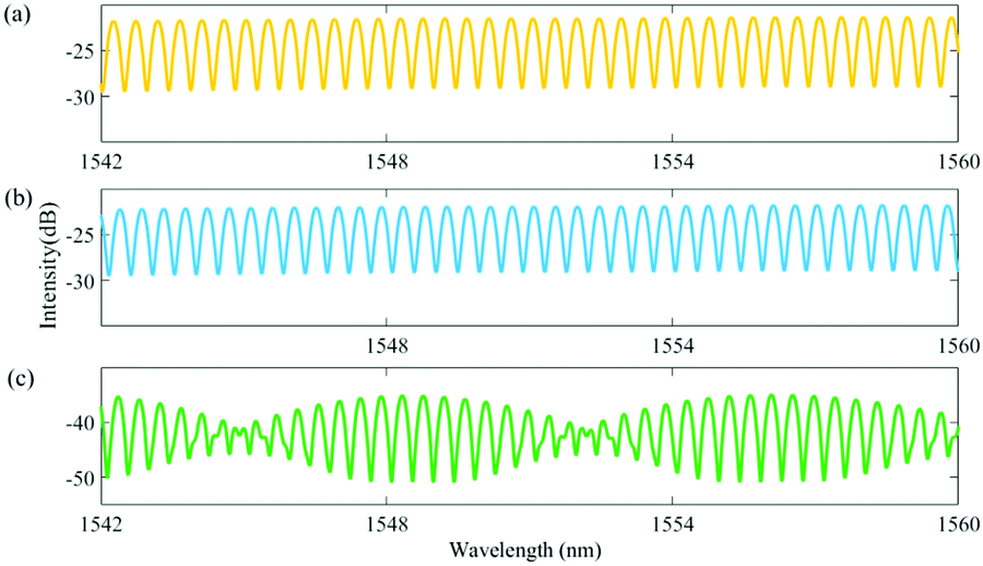 | ||
| Fig. 5 Spectra of Vernier-effect (0 mA): (a) reference MKR, (b) sensing MZI, and (c) cascaded sensors. | ||
The pump light generated by the laser diode is directly irradiated onto the InSe through a cylindrical lens. Due to the photothermal effect, the material absorbs the 980 nm pump light, thus generating a large amount of heat and varying the amount of refractive index. The sensing MZI achieves a spectral shift when pump light propagates in the material-based device. Finally, the phase of the signal light from the MKR is changed to achieve the wavelength shift. When the pump power is 108 mW, the wavelength shifts 0.49 nm (as shown in Fig. 6) and the corresponding cascaded system shifts 12.22 nm.
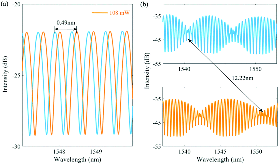 | ||
| Fig. 6 Spectral shifts of (a) sensing MZI and (b) cascaded configuration at the light intensity of 108 mW. | ||
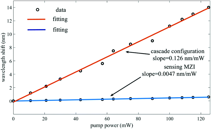
When the pump power increases from 0 mW to 126 mW, the wavelength of the single sensor MZI without Vernier effect moves by ∼2.7 nm. The sensitivity of the single sensor MZI is 0.0047 nm mW−1. For the entire Vernier-based cascade system, when the light power changed from 0–126 mW, the wavelength shifted by ∼14 nm. The sensitivity of the cascade system is 0.126 nm mW−1 (as shown in Fig. 7) and the calculated K of this system is 26.8, which is very close to the theoretical value.
 | ||
| Fig. 7 The relationship between the wavelength shifts and the light intensity of sensing MZI and cascade configuration. | ||
One attractive advantage of this system is that it can change the FSR of two MZIs through the delay line. When the value difference between FSRR and FSRS is small, the sensitivity of the system can be improved. On the other hand, due to various materials having different photothermal properties, other 2D materials can also be applied to this system. Thus, our work may open the doors for the application of 2D materials in cascade sensors.
Conclusion
In summary, we have successfully synthesized 2D few-layer InSe by a facile LPE method with the assistance of centrifugation. It was proved by photothermal response measurement that the few-layer InSe has excellent photothermal conversion efficiency compared with other 2D materials. In addition, considering the high surface-to-volume ratio, thermal stability, and direct bandgap for easy light coupling of InSe, a novel and economical sensitivity-enhanced Vernier-cascaded photothermal fiber sensor based on the few-layer InSe was constructed. Under irradiation of 980 nm pump light, the results show that the sensitivity of the cascaded sensor is 0.126 nm mW−1 while the sensitivity of the single sensing MZI is 0.0047 nm mW−1. When light intensity changes from 0–126 mW, the wavelength is shifted significantly by ∼14 nm. The experiments demonstrated the MZI–MKR Vernier sensor with ∼26.8 times sensitivity enhancement, which is basically consistent with the theoretical analysis. Our work not only brings 2D materials into optical cascade sensing fields but also may offer inspirations for applications in optical imaging, chemistry, and biomedicine.Author contributions
Rui Wang, Qing Wu, and Xiantao Jiang designed the experiments; Rui Wang and Qing Wu carried out the experiments; Rui Wang, Taojian Fan, Jia Guo, and Cong Wang assisted with InSe preparation and characterization; Rui Wang, Qing Wu, and Yali Gao analysed the experimental results; Rui Wang wrote the manuscript; Feng Zhang and Zhengqian Luo reviewed the manuscript; Han Zhang and Meng Zhang approved the final manuscript.Conflicts of interest
There are no conflicts to declare.Acknowledgements
The research was partially supported by the financial supports from the Science and Technology Development Fund (No. 007/2017/A1 and 132/2017/A3), Macao Special Administration Region (SAR), China, and National Natural Science Fund (Grant No. 61875138, 61435010, 6181101252, 51778030, and 51978024), and Science and Technology Innovation Commission of Shenzhen (KQTD2015032416270385, JCYJ20150625103619275, and JCYJ20170811093453105). The authors also acknowledge the support from Instrumental Analysis Center of Shenzhen University (Xili Campus).Notes and references
- K. S. Novoselov, A. K. Geim, S. V. Morozov, D. Jiang, Y. Zhang, S. V. Dubonos, I. V. Grigorieva and A. A. Firsov, Science, 2004, 306, 666–669 CrossRef CAS.
- W. Huang, C. Xing, Y. Wang, Z. Li, L. Wu, D. Ma, X. Dai, Y. Xiang, J. Li, D. Fan and H. Zhang, Nanoscale, 2018, 10, 2404–2412 RSC.
- X. Jiang, S. Liu, W. Liang, S. Luo, Z. He, Y. Ge, H. Wang, R. Cao, F. Zhang and Q. Wen, Laser Photonics Rev., 2018, 12, 1700229 CrossRef.
- W. F. Chen, K. Sasaki, C. Ma, A. I. Frenkel, N. Marinkovic, J. T. Muckerman, Y. Zhu and R. R. Adzic, Angew. Chem., Int. Ed., 2012, 51, 6131–6135 CrossRef CAS.
- L. Qu, Y. Liu, J.-B. Baek and L. Dai, ACS Nano, 2010, 4, 1321–1326 CrossRef CAS.
- S.-M. Paek, E. Yoo and I. Honma, Nano Lett., 2008, 9, 72–75 CrossRef.
- J. Zhu, D. Yang, Z. Yin, Q. Yan and H. Zhang, Small, 2014, 10, 3480–3498 CrossRef CAS.
- F. Schedin, A. Geim, S. Morozov, E. Hill, P. Blake, M. Katsnelson and K. Novoselov, Nat. Mater., 2007, 6, 652–655 CrossRef CAS PubMed.
- T. Wang, Y. Guo, P. Wan, H. Zhang, X. Chen and X. Sun, Small, 2016, 12, 3748–3756 CrossRef CAS.
- S. Bai, C. Sun, H. Yan, X. Sun, H. Zhang, L. Luo, X. Lei, P. Wan and X. Chen, Small, 2015, 11, 5807–5813 CrossRef CAS.
- S. Yang, Y. Liu, W. Chen, W. Jin, J. Zhou, H. Zhang and G. S. Zakharova, Sens. Actuators, B, 2016, 226, 478–485 CrossRef CAS.
- Z. Li, H. Qiao, Z. Guo, X. Ren, Z. Huang, X. Qi, S. C. Dhanabalan, J. S. Ponraj, D. Zhang, J. Li, J. Zhao, J. Zhong and H. Zhang, Adv. Funct. Mater., 2018, 28, 1705237 CrossRef.
- W. Feng, W. Zheng, W. W. Cao and P. A. Hu, Adv. Mater., 2014, 26, 6587–6593 CrossRef CAS.
- D. Martens and P. Bienstman, Nanophotonics, 2017, 6, 703–712 CAS.
- L.-Y. Shao, Y. Luo, Z. Zhang, X. Zou, B. Luo, W. Pan and L. Yan, Opt. Commun., 2015, 336, 73–76 CrossRef CAS.
- Q. Wang, W. Q. Wei, M. J. Guo and Y. Zhao, Sens. Actuators, B, 2016, 222, 159–165 CrossRef CAS.
- E. Reyes-Vera, C. M. B. Cordeiro and P. Torres, Appl. Opt., 2017, 56, 156–162 CrossRef CAS.
- Q. Wang, L. X. Kong, Y. L. Dang, F. Xia, Y. W. Zhang, Y. Zhao, H. F. Hu and J. Li, Sens. Actuators, B, 2016, 225, 213–220 CrossRef CAS.
- Y. Q. Wang, C. Y. Shen, W. M. Lou and F. Y. Shentu, Sens. Actuators, B, 2016, 234, 503–509 CrossRef CAS.
- Y. Yang, Y. Wang, Y. Zhao, J. Jiang, X. He, W. Yang, Z. Zhu, W. Gao and L. Li, Opt. Express, 2017, 25, 33290–33296 CrossRef CAS.
- Y. Geng, X. Li, X. Tan, Y. Deng and Y. Yu, IEEE Sens. J., 2011, 11, 2891–2894 Search PubMed.
- H. Liao, P. Lu, X. Fu, X. Jiang, W. Ni, D. Liu and J. Zhang, Opt. Express, 2017, 25, 26898–26909 CrossRef CAS PubMed.
- Q. Wang, C. Du, J. M. Zhang, R. Q. Lv and Y. Zhao, Opt. Commun., 2016, 377, 89–93 CrossRef CAS.
- Y. Zhao, F. Xia and J. Li, J. Lightwave Technol., 2016, 34, 1373–1379 CAS.
- N. L. P. Andrews, R. Ross, D. Munzke, C. van Hoorn, A. Brzezinski, J. A. Barnes, O. Reich and H. P. Loock, Opt. Express, 2016, 24, 14086–14099 CrossRef PubMed.
- N. Bozinovic, Y. Yue, Y. X. Ren, M. Tur, P. Kristensen, H. Huang, A. E. Willner and S. Ramachandran, Science, 2013, 340, 1545–1548 CrossRef CAS.
- H. Y. Choi, M. J. Kim and B. H. Lee, Opt. Express, 2007, 15, 5711–5720 CrossRef.
- Y. H. Luo, C. Y. Chen, K. Xia, S. H. Peng, H. Y. Guan, J. Y. Tang, H. U. Lu, J. H. Yu, J. Zhang, Y. Xiao and Z. Chen, Opt. Express, 2016, 24, 8956–8966 CrossRef CAS PubMed.
- L. P. Sun, J. Li, L. Jin, Y. Ran and B. O. Guan, Sens. Actuators, B, 2016, 231, 696–700 CrossRef CAS.
- X. Tu, J. Song, T.-Y. Liow, M. K. Park, J. Q. Yiying, J. S. Kee, M. Yu and G.-Q. Lo, Opt. Express, 2012, 20, 2640–2648 CrossRef CAS.
- B. Wu, C. Zhao, B. Xu and Y. Li, Sens. Actuators, B, 2018, 255, 3011–3016 CrossRef CAS.
- Z. Xu, Q. Sun, J. Wo, Y. Dai, X. Li and D. Liu, IEEE Sens. J., 2013, 13, 2139–2145 Search PubMed.
- Z. Y. Zhao, M. A. Soto, M. Tang and L. Thevenaz, Opt. Express, 2016, 24, 25211–25223 CrossRef PubMed.
- J. N. Coleman, M. Lotya, A. O'Neill, S. D. Bergin, P. J. King, U. Khan, K. Young, A. Gaucher, S. De, R. J. Smith, I. V. Shvets, S. K. Arora, G. Stanton, H.-Y. Kim, K. Lee, G. T. Kim, G. S. Duesberg, T. Hallam, J. J. Boland, J. J. Wang, J. F. Donegan, J. C. Grunlan, G. Moriarty, A. Shmeliov, R. J. Nicholls, J. M. Perkins, E. M. Grieveson, K. Theuwissen, D. W. McComb, P. D. Nellist and V. Nicolosi, Science, 2011, 331, 568–571 CrossRef CAS PubMed.
- R. Wang, X. Jiang, S. Gao, J. Zhao, F. Zhang, W. Huang, T. Fan, W. Liang, Z. Li, H. Huang, Z. Guo, H. Wang, Y. Zhang, X. Zhang, Z. Luo and H. Zhang, Adv. Mater. Interfaces, 2019, 6, 201900171 Search PubMed.
- D. Ma, J. Zhao, R. Wang, C. Xing, Z. Li, W. Huang, X. Jiang, Z. Guo, Z. Luo, Y. Li, J. Li, S. Luo, Y. Zhang and H. Zhang, ACS Appl. Mater. Interfaces, 2019, 11, 4278–4287 CrossRef CAS.
- M. Yuksek, U. Kurum, H. G. Yaglioglu, A. Elmali and A. Ates, J. Appl. Phys., 2010, 107, 033115 CrossRef.
- Y. Sun, S. Luo, X. G. Zhao, K. Biswas, S. L. Li and L. Zhang, Nanoscale, 2018, 10, 7991–7998 RSC.
- G. W. Mudd, S. A. Svatek, T. Ren, A. Patane, O. Makarovsky, L. Eaves, P. H. Beton, Z. D. Kovalyuk, G. V. Lashkarev, Z. R. Kudrynskyi and A. I. Dmitriev, Adv. Mater., 2013, 25, 5714–5718 CrossRef CAS PubMed.
- J. F. Sánchez-Royo, G. Muñoz-Matutano, M. Brotons-Gisbert, J. P. Martínez-Pastor, A. Segura, A. Cantarero, R. Mata, J. Canet-Ferrer, G. Tobias, E. Canadell, J. Marqués-Hueso and B. D. Gerardot, Nano Res., 2014, 7, 1556–1568 CrossRef.
- J. J. Wang, F. F. Cao, L. Jiang, Y. G. Guo, W. P. Hu and L. J. Wan, J. Am. Chem. Soc., 2009, 131, 15602–15603 CrossRef CAS PubMed.
- Z. Xie, D. Wang, T. Fan, C. Xing, Z. Li, W. Tao, L. Liu, S. Bao, D. Fan and H. Zhang, J. Mater. Chem. B, 2018, 6, 4747–4755 RSC.
- T. Fan, Y. Zhou, M. Qiu and H. Zhang, J. Innovative Opt. Health Sci., 2018, 11, 1830003 CrossRef CAS.
- T. Xue, W. Liang, Y. Li, Y. Sun, Y. Xiang, Y. Zhang, Z. Dai, Y. Duo, L. Wu and K. Qi, Nat. Commun., 2019, 10, 28 CrossRef.
- B. Wang, J. H. Wang, Q. Liu, H. Huang, M. Chen, K. Li, C. Li, X. F. Yu and P. K. Chu, Biomaterials, 2014, 35, 1954–1966 CrossRef CAS PubMed.
- C. M. Hessel, V. P. Pattani, M. Rasch, M. G. Panthani, B. Koo, J. W. Tunnell and B. A. Korgel, Nano Lett., 2011, 11, 2560–2566 CrossRef CAS PubMed.
- Z. Sun, H. Xie, S. Tang, X.-F. Yu, Z. Guo, J. Shao, H. Zhang, H. Huang, H. Wang and P. K. Chu, Angew. Chem., Int. Ed., 2015, 54, 11526–11530 CrossRef CAS.
- D. Meng, S. Yang, L. Guo, G. Li, J. Ge, Y. Huang, C. W. Bielawski and J. Geng, Chem. Commun., 2014, 50, 14345–14348 RSC.
- Z. Huang, Y. Qi, D. Yu and J. Zhan, RSC Adv., 2016, 6, 31031–31036 RSC.
- X. Jiang, L. Tong, G. Vienne, X. Guo, A. Tsao, Q. Yang and D. Yang, Appl. Phys. Lett., 2006, 88, 223501 CrossRef.
- L. M. Tong, Sensors, 2018, 18, 27 Search PubMed.
Footnote |
| † These authors contributed equally to this work. |
| This journal is © The Royal Society of Chemistry 2020 |