
 Open Access Article
 This Open Access Article is licensed under a Creative Commons Attribution-Non Commercial 3.0 Unported Licence
Localized surface plasmon effects on the photophysics of perovskite thin films embedding metal nanoparticles†
Aaron
Bayles
 a,
Sol
Carretero-Palacios
ab,
Laura
Calió
a,
Gabriel
Lozano
a,
Mauricio E.
Calvo
*a and
Hernán
Míguez
*a
a,
Sol
Carretero-Palacios
ab,
Laura
Calió
a,
Gabriel
Lozano
a,
Mauricio E.
Calvo
*a and
Hernán
Míguez
*a
aMultifunctional Optical Materials group, Institute of Materials Science of Seville, Consejo Superior de Investigaciones Científicas (CSIC) – Universidad de Sevilla (US), Américo Vespucio 49, 41092, Seville, Spain. E-mail: h.miguez@csic.es
bDept. Física de Materiales and Instituto Nicolás Cabrera, Universidad Autónoma de Madrid, Campus de Cantoblanco, 28049 Madrid, Spain
First published on 23rd December 2019
Abstract
Herein we provide direct experimental evidence that proves that the photophysical properties of thin methylammonium lead iodide perovskite films are significantly enhanced by localized surface plasmon resonances (SPRs). Observations are well supported by rigorous calculations that prove that improved light harvesting can be unequivocally attributed to plasmonic scattering and near field reinforcement effects around silver nanoparticles embedded within the semiconductor layer. Adequate design of the localized SPR allows raising the absorptance of a 300 nm thick film at well-defined spectral regions while minimizing the parasitic absorption from the metallic inclusions. Measured enhancements can be as large as 80% at specific wavelengths and 20% when integrated over the whole range at which SPR occurs, in agreement with theoretical estimations. Simultaneously, the characteristic quenching effect that the vicinity of metals has on the photoluminescence of semiconductors is largely compensated for by the combined effect of the enhanced photoexcitation and the higher local density of photon states occurring at SPR frequencies, with a two fold increase of the perovskite photoemission efficiency being measured.
Introduction
The interest generated by the fast progression of perovskite based optoelectronics has motivated diverse research communities to make an effort to contribute their expertise to improve the performance, versatility and adaptability of these devices. In this context, different approaches have been proposed from the perspective of the optical design to improve the aesthetics of perovskite solar cells,1–3 increase their light harvesting while reducing carrier recombination losses,4 or boost photon recycling.5,6 Also, inclusion of optical resonators and gratings in perovskite light emitting devices (LEDs) has lowered the excitation energy threshold for lasing or allowed the fabrication of high brightness white light LEDs.7–9 Among the various contributions from the field of photonics proposed to improve light harvesting efficiency, photoemission, or other concomitant effects such as carrier dynamics, those based on the use of plasmonic resonances stand as the most widely explored.10–14 In particular, numerous experimental works report the photovoltaic or photodetection performance enhancement that results from coupling metallic nanostructures to organic metal halide perovskite films.15–32 However, the origin of the improvement reported remains, in most cases, unclear. In some cases, inclusion of metallic nanoparticles has led to an increase of the cell efficiency without affecting the optical absorption of the perovskite, which remains unchanged, hence discarding light trapping as the mechanism behind the improvement.16,21,24,27 On the other hand, in those occasions in which light harvesting enhancement is observed, the absorptance and the external quantum efficiency reported show no clear spectral fingerprint of a well-defined plasmonic resonance.5,18,19,22,25,26,29 This is surprising since, regardless of the origin of the radiative coupling between the host and the metallic guest, which could be mainly caused by scattering, near field enhancement or both, its effect on absorptance should be limited to those spectral ranges at which the surface plasmon resonance (SPR) occurs.10 This might be very likely due to the difficulties typically encountered to achieve a strict control over the geometry of the materials involved, which also prevents an adequate comparison between reference and sample, complicating the fine analysis and quantification of the observed effects.In this work, we present clear experimental evidence that proves that metallic nanoparticles embedded in perovskite thin films give rise to enhancement of absorption at well-defined spectral ranges. We prove that such reinforcement is due to the strong light–matter interaction produced by the localization of electromagnetic modes, rather than scattering, around the particles when localized SPRs are excited. Films have been carefully prepared and selected to ensure precise control over their thickness, thus providing an adequate platform for the comparative analysis herein proposed. Silver particles are embedded in a series of perovskite films of similar, and equally controlled, thickness. Significant reinforcement of the absorptance is detected exclusively at those wavelength ranges in which calculations predict strong near field enhancement around the metallic inclusions, hence strongly supporting the hypothesis that the observed light harvesting increase has a purely plasmonic origin. This increase can be as large as 80% at the maximum resonant frequencies and 20% when integrated over the whole spectral range at which the localized SPR extends. Furthermore, significantly more intense photoluminescence (PL) is observed at those same spectral ranges, as a result of the synergistic effect of enhanced photoexcitation and the larger density of radiative modes available in the vicinity of the metal particles.
Results and discussion
Films were prepared following the general guidelines reported in ref. 10, in which a thorough computational screening of the effect of different compositions and sizes of both bare and core–shell nanoparticles on the absorption of methylammonium lead iodide (MAPI) perovskite films of diverse thickness was carried out. The reliability of the model and simulation method employed there was already confirmed by contrasting its outcome with previous observations of plasmonic effects in perovskite solar cells, which could be rationalized and fitted for the first time.16 Some predictions of this model are that silver nanoparticles present the greatest potential to provide the largest absorption enhancement, and that ample ranges of relatively large metallic nanoparticles (sizes >50 nm) at low concentrations (<10%) should be embedded within thin perovskite films (<300 nm) in order to observe a significant enhancement of light harvesting by the semiconductor. Bigger particles present localized SPRs at longer visible wavelengths, at which perovskite absorption coefficient is lower; also, although the peak field enhancements attained for larger metallic particles are lower than for smaller ones, the perovskite volume in which light trapping takes place is larger, which favours a more efficient light harvesting. With these considerations in mind, 70 nm diameter silver particles of cubic shape were synthesized employing well-tested techniques in the field,33–35 both bare (np-Ag) and coated with a thin silica shell (np-Ag@SiO2). Then, they were dispersed in ethanol and deposited onto flat substrates by spin coating. After that, a MAPI precursor solution in a mixture of N,N-dimethylformamide and dimethyl sulfoxide (ratio 4![[thin space (1/6-em)]](https://www.rsc.org/images/entities/char_2009.gif) :1) was spun onto them and thermally annealed at 100 °C to obtain highly planar thin (300 nm) perovskite films with metallic inclusions. Filling fractions of np-Ag and np-Ag@SiO2 in the perovskite film are expected to be around 5%, as extracted from the analysis of field emission scanning electron microscopy (FESEM) images of the metal particle deposited surfaces prior to MAPI formation. These values should give rise to a measurable enhancement of the light harvesting efficiency of the perovskite.37 Full details of the preparation procedure followed are given in the Methods section. This protocol allows us to attain sets of uniform slabs of similar thickness, as required for the analysis herein proposed. A transmission electron microscopy (TEM) image of a np-Ag@SiO2 is displayed in Fig. 1(a). Lateral and top FESEM views of the result of depositing these particles onto a silicon wafer can be seen in Fig. 1(b) and (c). A cross section of the film attained after synthesizing the MAPI perovskite layer, as observed by FESEM, is depicted in Fig. 1(d). Note that the fingerprints of embedded particles are detected as cavities in the picture, since they are removed as a result of sample cleavage and exposition under electron beam. As reference, films of pure MAPI of the exact same thickness were prepared. In Fig. S1 (ESI†), we disclose both SEM cross section images and surface profile measurements of a sample and reference, in which it can be seen that film thickness and roughness are similar in both films.
:1) was spun onto them and thermally annealed at 100 °C to obtain highly planar thin (300 nm) perovskite films with metallic inclusions. Filling fractions of np-Ag and np-Ag@SiO2 in the perovskite film are expected to be around 5%, as extracted from the analysis of field emission scanning electron microscopy (FESEM) images of the metal particle deposited surfaces prior to MAPI formation. These values should give rise to a measurable enhancement of the light harvesting efficiency of the perovskite.37 Full details of the preparation procedure followed are given in the Methods section. This protocol allows us to attain sets of uniform slabs of similar thickness, as required for the analysis herein proposed. A transmission electron microscopy (TEM) image of a np-Ag@SiO2 is displayed in Fig. 1(a). Lateral and top FESEM views of the result of depositing these particles onto a silicon wafer can be seen in Fig. 1(b) and (c). A cross section of the film attained after synthesizing the MAPI perovskite layer, as observed by FESEM, is depicted in Fig. 1(d). Note that the fingerprints of embedded particles are detected as cavities in the picture, since they are removed as a result of sample cleavage and exposition under electron beam. As reference, films of pure MAPI of the exact same thickness were prepared. In Fig. S1 (ESI†), we disclose both SEM cross section images and surface profile measurements of a sample and reference, in which it can be seen that film thickness and roughness are similar in both films.
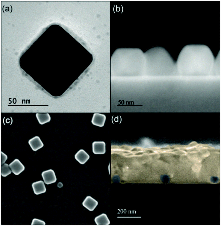 | ||
| Fig. 1 (a) TEM image of a np-Ag@SiO2; FESEM image of (b) side and (c) top views of Ag@SiO2 particles deposited onto a silicon wafer; (d) FESEM image of a cross section of the resulting np-Ag@SiO2 loaded perovskite film attained. | ||
Total reflectance (R) and total transmittance (T) of both reference and metal particle loaded films were collected with an integrating sphere attached to a spectrophotometer. Then, optical absorptance (A) was estimated as A = 1 − R − T. Fig. 2(a) displays a sequence of absorptance spectra obtained from a perovskite thin film loaded with np-Ag and np-Ag@SiO2 at different times after sample preparation. All three R, T and A for a film containing np-Ag@SiO2 are provided as ESI,† (Fig. S2). Freshly prepared films present, when compared to reference ones, an intense and well-defined absorption enhancement band at red wavelengths. The sequential changes observed in the absorptance reveals that uncoated np-Ag undergo a gradual degradation when embedded within MAPI. Interestingly, the sample ends up showing an optical response that resembles that of the reference film, where no silver particles were introduced. On the other hand, the absorptance of slabs embedding np-Ag@SiO2 showed significantly less degradation, albeit less initial enhancement, than the np-Ag ones. Simulated spectra, calculated following a procedure reported before10,36 and using as input the parameters extracted from electron microscopy analysis, are depicted in Fig. 2(b). In these fittings, the only free parameter is the metal particle concentration, which is found to be 5.8%, in good agreement with the estimations based on the analysis of FESEM images. The absorptance due to parasitic absorption by the metal inclusion is also plotted for the sake of comparison. The comparison between experimental and theoretical results (which consider the particles as isolated) is excellent, discarding any eventual agglomeration effect. Please notice that these simulations demonstrate that the significant increase of absorption observed in the red region of the spectrum occurs in the perovskite and not in the metal particles. In Fig. 2(c), we plot compared the experimentally observed and the theoretically expected absorptance enhancements, an excellent qualitative and quantitative agreement between them being found. In order to discard spurious effects caused by small film thickness variations between sample and reference, we also analysed the effect on the absorptance of a pure MAPI film of gradually increasing film thickness in 20 nm steps, starting with a 300 nm thick slab. Results are plotted in Fig. 2(d) and serve to confirm that the experimental enhancement observed in Fig. 2(a) cannot be attributed to potential variations of film thickness between sample and reference. Since these thicknesses are equal, the amount of perovskite in the sample is even slightly less than that present in the reference, as part of the perovskite volume present in the latter is replaced by the embedded metal particles.
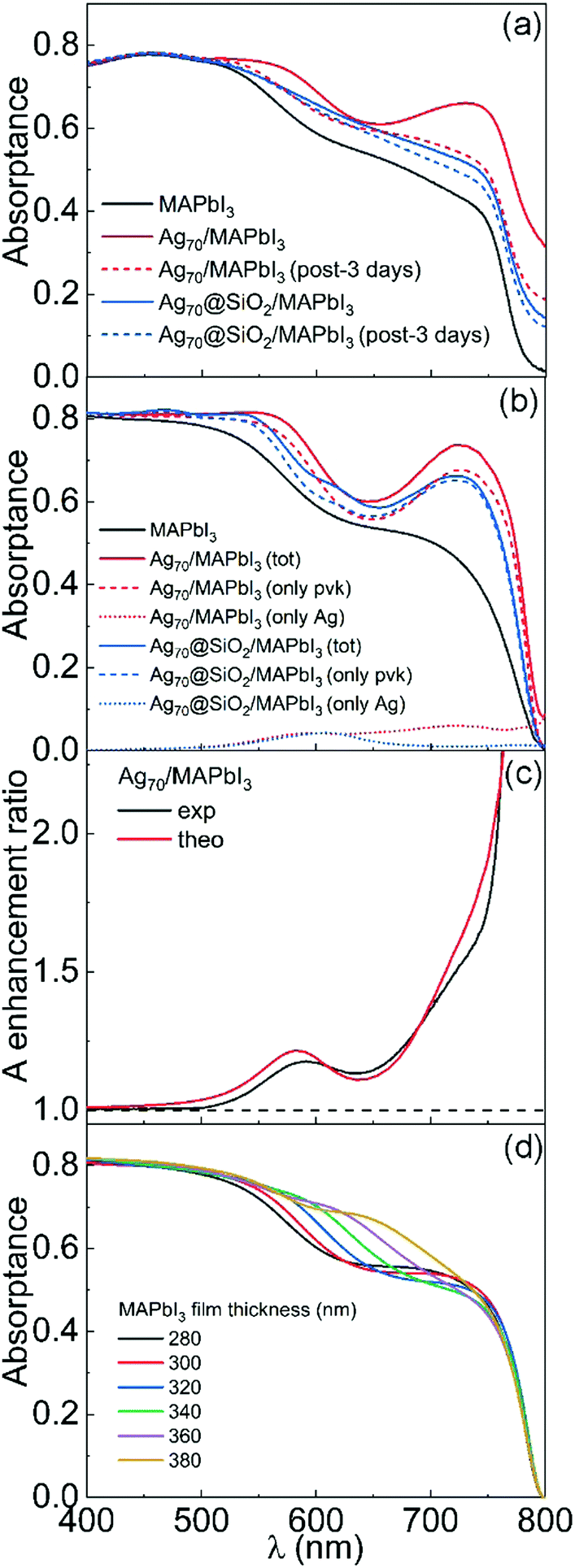 | ||
| Fig. 2 (a) Experimental and (b) simulated absorptance spectra of MAPI perovskite films both pure (black solid line, used as reference) and loaded with np-Ag (red solid line) and np-Ag@SiO2 (blue solid line); in (b), the absorption occurring within the perovskite material and the silver particles is discriminated and separately plotted as dashed and dotted lines, respectively. (c) Spectral dependence of the experimental (red line) and simulated (black line) total film absorptance (A) enhancement attained for a np-Ag MAPI film when compared to a reference pure MAPI film. (d) Simulated absorptance spectra showing the effect of gradually increasing thickness of a MAPI film from 280 nm to 380 nm. | ||
At the same time, it shows that strict control over this parameter is required in order to reach a meaningful conclusion on the effect of metal particles, since an increase in film width can also give rise to absorption enhancements in well-defined spectral regions that can be mistakenly attributed to an optical resonance. This is explicitly shown in Fig. S3 (ESI†), in which the simulated enhancement spectra expected for pure films whose thickness range between 320 nm and 380 nm is plotted. Further analysis on the dependence of the enhancement observed on other parameters, such as particle concentration or silica coating thickness is presented in Fig. S4 (ESI†).
In order to elucidate the origin of the enhancement observed, we calculated the spatial distribution of both the electric field intensity and the power absorbed along a cross section of one of the films that simulate the structures actually built at the maximum absorption wavelength (i.e., λ = 725 nm). By doing so, we can discriminate between the two possible radiative plasmonic effects that could give rise to absorption, i.e., scattering and near field enhancement. The results are shown in Fig. 3. Analysis of these plots indicates that both radiative plasmonic effects, field reinforcement around the surface of the metal inclusions and scattering, are responsible for the enhancement of absorption experimentally observed. It also explicitly shows the small absorption occurring within the metal at red wavelengths. Specifically, averaging over several cubic volumes near and around the metal particle, it is found that near field effects are responsible for 20% of the enhancement observed, while far field effects contribute with 80%.
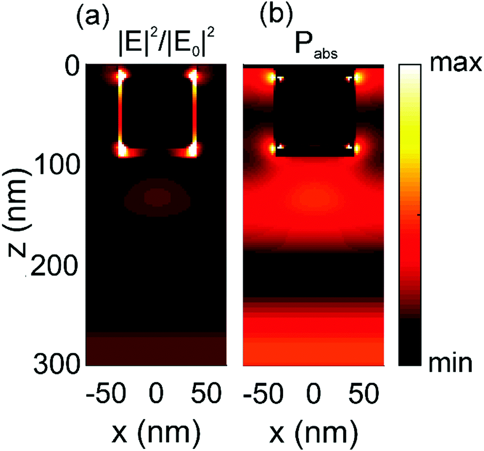 | ||
| Fig. 3 (a) Spatial distribution of the normalized electric field intensity and (b) the absorbed power per unit volume (Pabs) attained at λ = 725 nm for a silver nanocube of 70 nm side with 9 nm thick SiO2 shell, in a perovskite layer of 300 nm (6% filling fraction). In these graphs, light enters the film from below, the bottom of the film being located at z = 0 nm. | ||
Finally, we investigated the effect that the presence of metal particles might have on the photoemission of the metal halide perovskite. Again, as in the case of the absorptance, the presence of metal particles may have opposite effects on the efficiency of the photoemission. On the one hand, the proximity of metals to light emitting materials may cause the quenching of the luminescence by electron scavenging, plasmon induced energy transfer or reabsorption. On the other, the already discussed enhanced absorption at excitation frequencies and the higher density of optical states at emission frequencies should improve the PL intensity. This latter effect results from the increased radiative recombination rate of excited electrons in an emitter as a result of the enhanced photon local density of states (LDOS) around the metal particles, a phenomenon that has been thoroughly described for different types of emitters embedded in a photonic environment.37 Photon LDOS depends exclusively on the optical environment surrounding the emitter, which is in turn determined by the spatial modulation of the complex refractive index around it.38 Hence the balance between the two mentioned antagonistic effects is expected to determine the photoexcitation and photoemission spectra of the metal particle loaded perovskite film. The PL spectra for both bare and metal loaded MAPI films attained employing a wide range of pumping wavelengths (400 nm < λexc < 650 nm) are plotted in Fig. 4(a) and (b), respectively (a comparison between selected PL spectra attained from the different films under study using the same photoexcitation is shown in Fig. S5, ESI†). Interestingly, when the films are photoexcited with λexc below the spectral region at which plasmonic absorption enhancement occurs, photoemission is poorer in the metal loaded film than in the reference. This picture is gradually reversed as λexc enters such region, in which reinforcement of absorptance is expected, integrated PL enhancement factors as large as 2 being attained, as illustrated in Fig. 4(c). Please note that this improvement cannot be explained exclusively by the increase in optical absorption. For instance, integrated PL enhancement is 75% for λexc = 530 nm while the absorptance reinforcement is only 5% at such wavelength. Our hypothesis is that a complex interplay between the spatial distribution of high absorption and high LDOS regions (whose increase is expected to be above 50% with respect to the reference film) is responsible for the large PL enhancements observed. Evidence of the higher LDOS is also found when time resolved PL decay measurements from bare and np-Ag@SiO2 loaded films, displayed in Fig. 4(d), are compared. Although a more complete description should be employed in order to offer a rigorous interpretation of the PL decay dynamics in organic lead halides,39 the comparison between the PL decay curves from metal loaded films and those attained for bare perovskite films based on a simple model clearly shows that shorter lifetimes accompany the higher emission intensities observed for metallic particle loaded films. Indeed, the estimated excited state lifetime is a 25% shorter (435 ns in the silver loaded film vs. 573 ns in the reference). This simultaneous observation of higher PL intensities and faster recombination is in good agreement with the occurrence of a larger number of radiative decay paths expected as a result of an increase in the photon LDOS.37,38 It should be remarked that, as organic lead halide perovskites show a recombination regime that is dictated by the excitation power and are also easily photodegraded, in our experiments we keep the optical pump as constant and low as possible (see methods), which allows us to discard any effect of the excitation power on the effects observed.
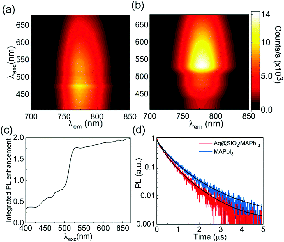 | ||
| Fig. 4 Photoluminescence (PL) spectra for 300 nm thick (a) pure MAPI (reference) and (b) np-Ag@SiO2 loaded MAPI (sample) films. Spectra were attained employing different pumping wavelengths, with λexc ranging from 400 nm to 650 nm. (c) Integrated PL enhancement vs. λexc attained from the comparison sample and reference. (d) Normalized PL decay curves measured for sample (red curve) and reference (blue curve). | ||
Conclusions
In conclusion, we have provided direct and unambiguous experimental evidence of radiative plasmonic enhancement of both optical absorption and photoemission of an organic metal halide perovskite thin film embedding metal nanoparticles. In order to do so, a careful theoretical design had to be followed and a strict control over nanoparticle size and film thickness achieved. Optical characterization of thin perovskite slabs containing either bare or silica coated silver particles shows that plasmonic enhancement effects take place in well-defined spectral regions, in excellent agreement with theoretical predictions. Our research provides a reliable measure of the magnitude of the plasmonic enhancement effects expected for optoelectronic devices based on perovskite thin films.Methods
Chemicals
Silver nitrate (AgNO3, ≥99%), polyvinylpyrrolidone (PVP, MW = 55000), ethylene glycol (EG, ≥99.8%), tetraethyl orthosilicate (TEOS, ≥99%), ammonia water (NH3(aq), 28%), methylammonium iodide (MAI, 99.9%), dimethyl sulfoxide (DMSO) and N,N-dimethylformamide (DMF) were obtained from Sigma-Aldrich and used as received without any purification. Lead iodide (PbI2, 99.8%) was purchased from TCI and used as received.
Silver nanocube (np-Ag) synthesis
Ag nanocubes of 70 nm of side length were synthesized accordingly to a previously reported procedure.34 Briefly, 1 mL of EG was preheated at 140 °C in an oil bath for 10 min; after that, 50 μL of 60 mM (3 μmol) HCl solution in EG was added into the vial and was left stirring for 3 minutes. Afterward, 1 mL of 0.2 M (200 μmol) AgNO3 solution in EG was added dropwise into the vial, with vigorous stirring. After another 3 min, 1 mL of 0.12 M (120 μmol) PVP solution in EG was slowly added dropwise to the solution. The vial was maintained uncapped for 3.5 hours and then capped for 95 min more, during continuous stirring at 140 °C in an oil bath. The product was then quenched in a water bath at room temperature for 20 min and washed several times with acetone and distilled water.SiO2 coating of Ag nanocubes (np-Ag@SiO2)
A thin coating of SiO2 (9 nm) was achieved through the Stöber process, as previously reported.35 The dispersion of Ag nanocubes in water was sonicated during 1 minute and thereafter 125 μL of TEOS were added to the dispersion. After sonicating for two minutes, the solution was injected into stirring solution of 3 mL of EtOH with 250 μL of ammonia solution (32%). The solution was kept stirring for 8–10 min, then quenched by pouring it in 40 mL of EtOH. The product was cleaned by several washing and centrifugations with absolute ethanol.Perovskite film synthesis
Perovskite film was deposited by spin coating from a precursor solution prepared by mixing 0.502 g of PbI2 with 0.179 g of MAI in 1.6 g of a 4:1 (v/v) DMF:DMSO solution. Once the salts were fully dissolved, the solution was deposited either on top of the glass substrate (for reference sample) or above the previously deposited nanoparticle film. The Ag or Ag@SiO2 nanoparticle loaded film was prepared by spin coating the dispersion of the nanoparticles with a three-step program: first, the solution was spin coated at 500 rpm for 10 s, then at 1000 rpm for 15 s and finally at 2000 rpm for 20 s. For the perovskite film deposition, a two-step spin coating program was used: the solution was first spin coated at 1000 rpm for 10 s and then at 3000 rpm for 30 s. 230 μL of chlorobenzene were dropped on top of the surface during the spinning process after 15 s.
Optical characterization
Total transmittance (TT) and total reflectance (TR) of perovskite films were measured with an integrating sphere (DRA-2500, Agilent) attached to a UV-Vis-NIR spectrophotometer (Cary 5000, Agilent). The photoexcitation and photoemission spectra and photoluminescence dynamics were measured with a spectrofluorometer (FLS1000, Edinburgh Instruments). The output optical power of the Xenon lamp at every excitation wavelength employed is low enough (<2 mW cm−2) to ensure the stability of the films, as we could confirm both by visual inspection and from the stability and reproducibility of the measurements. All results presented in Fig. 4 have been corrected to account for these spectral variation of the optical power.Numerical calculations
Three-dimensional (3D) finite-difference time-domain (FDTD) simulations are performed using the software FDTD Solutions from Lumerical Solutions.40 The system is illuminated by a plane wave impinging directly on the perovskite film. Absorption spectra are evaluated independently using the Advanced Method by Lumerical employing the expression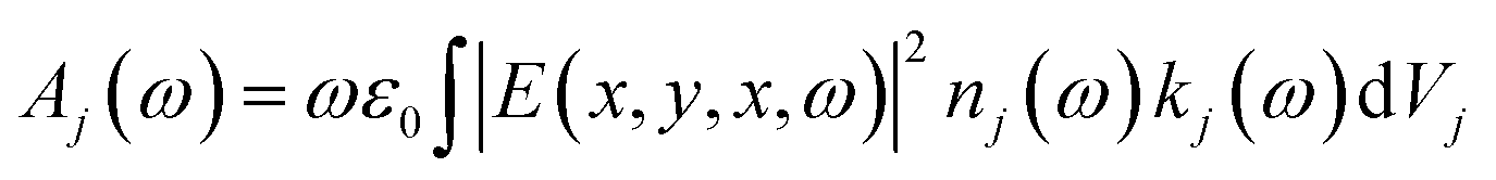 , with ω the angular frequency and E the electric field vector; nj(ω) and kj(ω) stand for the spectral-dependent real and imaginary parts of the refractive index of the material,36 a Johnson and Christy model for silver, and setting nSiO2(ω) = 1.5, for both the shell around Ag nanocubes and the glass substrate; Vj is the corresponding material volume. For the simulations, we consider Ag nanocubes of 70 nm size either bare or coated with a conformal SiO2 shell of 9 nm length, embedded in a 300 nm perovskite film and deposited on top of a glass substrate. A simulation box size of 1100 × 140 × 140 nm3 (of which 300 × 140 × 140 nm3 correspond to the film unit cell), with perfectly matching layer conditions on the boundary along plane wave injection, and symmetry ones along the remaining two, are considered. High density mesh ensuring converged results, with a minimum mesh refinement of 0.2 nm around the plasmonic nanoparticles, is taken.
Conflicts of interest
There are no conflicts to declare.Acknowledgements
The research leading to these results has received funding from the Spanish Ministry of Economy and Competitiveness under grant MAT2017-88584-R (AEI/FEDER,UE). A. B. was supported by the U. S. Department of State through the Fulbright Program. S. C. P. is grateful for the support of the AEI under the Juan de la Cierva Incorporación programme (IJCI-2016-28549).References
- W. Zhang, M. Anaya, G. Lozano, M. E. Calvo, M. B. Johnston, H. Míguez and H. J. Snaith, Nano Lett., 2015, 15, 1698–1702 CrossRef CAS PubMed.
- D. Liu, L. Wang, Q. Cui and L. J. Guo, Adv. Sci., 2018, 5, 1–9 Search PubMed.
- Y. Deng, Q. Wang, Y. Yuan and J. Huang, Mater. Horiz., 2015, 2, 578–583 RSC.
- N. Han, T. Ji, W. Wang, G. Li, Z. Li, Y. Hao, Y. Wu and Y. Cui, Org. Electron., 2019, 74, 190–196 CrossRef CAS.
- M. Saliba, W. Zhang, V. M. Burlakov, S. D. Stranks, Y. Sun, J. M. Ball, M. B. Johnston, A. Goriely, U. Wiesner and H. J. Snaith, Adv. Funct. Mater., 2015, 25, 5038–5046 CrossRef CAS.
- S. Nanz, R. Schmager, M. G. Abebe, C. Willig, A. Wickberg, A. Abass, G. Gomard, M. Wegener, U. W. Paetzold and C. Rockstuhl, APL Photonics, 2019, 4, 076104 CrossRef.
- N. Pourdavoud, T. Haeger, A. Mayer, P. J. Cegielski, A. L. Giesecke, R. Heiderhoff, S. Olthof, S. Zaefferer, I. Shutsko, A. Henkel, D. Becker-Koch, M. Stein, M. Cehovski, O. Charfi, H. Johannes, D. Rogalla, M. C. Lemme, M. Koch, Y. Vaynzof, K. Meerholz, W. Kowalsky, H. Scheer, P. Görrn and T. Riedl, Adv. Mater., 2019, 31, 1903717 CrossRef PubMed.
- Y. Liu, W. Yang, S. Xiao, N. Zhang, Y. Fan, G. Qu and Q. Song, ACS Nano, 2019, 13, 10653–10661 CrossRef CAS PubMed.
- L. Wang, L. Meng, L. Chen, S. Huang, X. Wu, G. Dai, L. Deng, J. Han, B. Zou, C. Zhang and H. Zhong, J. Phys. Chem. Lett., 2019, 10, 3248–3253 CrossRef CAS PubMed.
- S. Carretero-Palacios, A. Jiménez-Solano and H. Míguez, ACS Energy Lett., 2016, 1, 323–331 CrossRef CAS PubMed.
- E. S. Arinze, B. Qiu, G. Nyirjesy and S. M. Thon, ACS Photonics, 2016, 3, 158–173 CrossRef CAS.
- B. Liu, R. R. Gutha, B. Kattel, M. Alamri, M. Gong, S. M. Sadeghi, W.-L. Chan and J. Z. Wu, ACS Appl. Mater. Interfaces, 2019, 11, 32301–32309 CrossRef CAS PubMed.
- K. Kim and S. Lee, Opt. Express, 2019, 27, A1241 CrossRef CAS PubMed.
- E. Tiguntseva, A. Chebykin, A. Ishteev, R. Haroldson, B. Balachandran, E. Ushakova, F. Komissarenko, H. Wang, V. Milichko, A. Tsypkin, D. Zuev, W. Hu, S. Makarov and A. Zakhidov, Nanoscale, 2017, 9, 12486–12493 RSC.
- W. R. Erwin, H. F. Zarick, E. M. Talbert and R. Bardhan, Energy Environ. Sci., 2016, 9, 1577–1601 RSC.
- W. Zhang, M. Saliba, S. D. Stranks, Y. Sun, X. Shi, U. Wiesner and H. J. Snaith, Nano Lett., 2013, 13, 4505–4510 CrossRef CAS PubMed.
- N. Fu, Z. Y. Bao, Y. L. Zhang, G. Zhang, S. Ke, P. Lin, J. Dai, H. Huang and D. Y. Lei, Nano Energy, 2017, 41, 654–664 CrossRef CAS.
- N. K. Pathak, N. Chander, V. K. Komarala and R. P. Sharma, Plasmonics, 2017, 12, 237–244 CrossRef CAS.
- C. Ma, C. Liu, J. Huang, Y. Ma, Z. Liu, L.-J. Li, T. D. Anthopoulos, Y. Han, A. Fratalocchi and T. Wu, Sol. RRL, 2019, 3, 1900138 CrossRef.
- B. Du, W. Yang, Q. Jiang, H. Shan, D. Luo, B. Li, W. Tang, F. Lin, B. Shen, Q. Gong, X. Zhu, R. Zhu and Z. Fang, Adv. Opt. Mater., 2018, 6, 1701271 CrossRef.
- Q. Luo, C. Zhang, X. Deng, H. Zhu, Z. Li, Z. Wang, X. Chen and S. Huang, ACS Appl. Mater. Interfaces, 2017, 9, 34821–34832 CrossRef CAS PubMed.
- X. Ma, B. Ma, T. Yu, X. Xu, L. Zhang, W. Wang, K. Cao, L. Deng, S. Chen and W. Huang, ACS Appl. Energy Mater., 2019, 2, 3605–3613 CrossRef CAS.
- K. Yao, H. Zhong, Z. Liu, M. Xiong, S. Leng, J. Zhang, Y. X. Xu, W. Wang, L. Zhou, H. Huang and A. K. Y. Jen, ACS Nano, 2019, 13, 5397–5409 CrossRef CAS PubMed.
- H. L. Hsu, T. Y. Juang, C. P. Chen, C. M. Hsieh, C. C. Yang, C. L. Huang and R. J. Jeng, Sol. Energy Mater. Sol. Cells, 2015, 140, 224–231 CrossRef CAS.
- S. Panigrahi, S. Jana, T. Calmeiro, D. Nunes, J. Deuermeier, R. Martins and E. Fortunato, J. Mater. Chem. A, 2019, 7, 19811–19819 RSC.
- S. S. Mali, C. S. Shim, H. Kim, P. S. Patil and C. K. Hong, Nanoscale, 2016, 8, 2664–2677 RSC.
- H. Dong, T. Lei, F. Yuan, J. Xu, Y. Niu, B. Jiao, Z. Zhang, D. Ding, X. Hou and Z. Wu, Org. Electron., 2018, 60, 1–8 CrossRef CAS.
- S. Wang, J. Fang, C. Zhang, S. Sun, K. Wang, S. Xiao and Q. Song, Adv. Opt. Mater., 2017, 5, 1700529 CrossRef.
- H. Yu, J. Roh, J. Yun and J. Jang, J. Mater. Chem. A, 2016, 4, 7322–7329 RSC.
- D. Li, D. Zhou, W. Xu, X. Chen, G. Pan, X. Zhou, N. Ding and H. Song, Adv. Funct. Mater., 2018, 28, 1804429 CrossRef.
- H. Wang, J. W. Lim, L. N. Quan, K. Chung, Y. J. Jang, Y. Ma and D. H. Kim, Adv. Opt. Mater., 2018, 6, 1701397 CrossRef.
- K. Chan, M. Wright, N. Elumalai, A. Uddin and S. Pillai, Adv. Opt. Mater., 2017, 5, 1600698 CrossRef.
- L. Polavarapu and L. M. Liz-Marzán, Nanoscale, 2013, 5, 4355–4361 RSC.
- S. J. Jeon, J. H. Lee and E. L. Thomas, J. Colloid Interface Sci., 2014, 435, 105–111 CrossRef CAS PubMed.
- M. Lismont, C. A. Páez and L. Dreesen, J. Colloid Interface Sci., 2015, 447, 40–49 CrossRef CAS PubMed.
- S. Carretero-Palacios, M. E. Calvo and H. Míguez, J. Phys. Chem. C, 2015, 119, 18635–18640 CrossRef CAS PubMed.
- A. Jiménez-Solano, J. F. Galisteo-López and H. Míguez, J. Phys. Chem. Lett., 2018, 9, 2077–2084 CrossRef PubMed.
- L. Novotny and B. Hecht, Principles of Nano-Optics, Cambridge University Press, Cambridge, UK, 2006 Search PubMed.
- V. S. Chirvony and J. P. Martínez-Pastor, J. Phys. Chem. Lett., 2018, 9, 4955–4962 CrossRef CAS PubMed.
- Lumerical Inc., https://www.lumerical.com/products/.
Footnote |
| † Electronic supplementary information (ESI) available: Integrating sphere optical measurements, dependence of absorptance spectra and enhancements on different parameters and further analysis of the plasmonic effect on the photoemission. See DOI: 10.1039/c9tc05785d |
| This journal is © The Royal Society of Chemistry 2020 |