High stress-driven voltages in net-like layer-supported organic–inorganic perovskites

Rogers Tusiime a, Fatemeh Zabihi a, Mike Tebyetekerwa b, Yasmin Mohamed Yousry c, Yue Wu d, Morteza Eslamian ae, Shengyuan Yang a, Seeram Ramakrishna c, Muhuo Yu a and Hui Zhang *a
aState Key Laboratory for Modification of Chemical Fibers and Polymer Materials, International Joint Laboratory for Advanced Fiber and Low-dimension Materials, College of Materials Science and Engineering, Donghua University, Shanghai 201620, P. R. China. E-mail: zhanghui@dhu.edu.cn
bResearch School of Electrical, Energy and Materials Engineering, College of Engineering and Computer Science, Australian National University, Canberra 2601, Australia
cCentre for Nanofibers and Nanotechnology, National University of Singapore, Singapore 117581, Singapore
dResearch Center for Analysis and Measurement, Donghua University, Shanghai 201620, P. R. China
eUniversity of Michigan-Shanghai Jiaotong University Joint Institute, Shanghai 200240, P. R. China

Received 7th October 2019 , Accepted 2nd November 2019

First published on 7th November 2019


Abstract

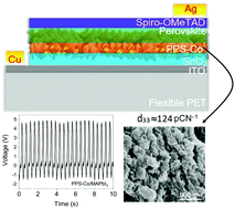
Hybrid organo-metal halide perovskites (OMHPs) have been extensively explored for photo or photo-enhanced applications, which are time, location or light-limited. Unlike in other works, herein, methylammonium lead iodide (MAPbI3) perovskite was employed as a small area (<1 cm2) stress-driven energy converter. Briefly, MAPbI3 was infiltrated into a net-like composite scaffold, having three constituents; polyvinylidene fluoride (PVDF), polylactic acid (PLA) and tin dioxide (SnO2) electrospun nanofibres. A systematic vertical ultrasonic vibration was optimized and applied to each sample, followed by ice quenching. Addition of MAPbI3 and vertical vibration altered the morphotropic phase nature of the composite towards desirable electroactive forms, without further poling, revealed by XRD, FTIR, and Raman studies. When the device was subjected to bending/compression-release forces, high output voltage of 4.82 V and current of 29.7 nA were obtained over an area of 0.0625 cm2. The champion device also registered high piezoelectric strain coefficients (d33) of 123.93 pC N−1 and 118.85 pC N−1 (with and without a SnO2 nanoparticle underlayer, respectively). We further elucidate the mechano-electrical outputs of MAPbI3 devices grown on other distinctive underlayers. This work advances the drive towards all-day–all-night energy harvesting using OMHPs, the force being applied from ubiquitous motions or artificial movements.


Driven by a skyrocketing demand for both handy and miniaturized smart, healthcare, and info/edutainment electronics, military and wearable devices and sensor systems, there has been tremendous interest in small area energy devices that have the potential to harness electrical output from several omnipresent processes.1,2 Similar to thermoelectrics and photovoltaics, piezoelectrics which convert mechanical energy to electrical energy and vice versa have also attracted researchers’ attention lately.3–5 Piezoelectrics have a non-centrosymmetric crystal morphology that facilitates displacement of dipoles on application of stress. In the years from the first discovery of piezoelectricity in 1880,6 enormous efforts have been commissioned towards improving this scientific marvel to performance levels supportive of ever-intricating user devices and systems. For instance, lower piezoelectric coefficients (d33 < 100 pC N−1) initially discovered in barium titanate, BaTiO3 – a perovskite structured ceramic7 have been tuned by over sixfold in Ba(Ti0.8Zr0.2)O3–(Ba0.7Ca0.3)TiO3 (d33 = 620 pC N−1).8 Many Pb-containing perovskite ceramics like lead zirconate titanate (PZT) have similarly been tuned using various intrinsic and extrinsic techniques presenting high piezoelectric coefficients.9,10 However, most of the present devices typically necessitate the piezoelectric material to be thin, soft, flexible and sturdy (to sustain many mechanical stress cycles). This is in addition to them having distinctive domains and domain walls. Conventional inorganic piezoelectrics (ceramics) are characteristically multidomain but grow at elevated temperatures in the paraelectric phase, and thus require additional high voltage poling and expensive processing steps to impart most of these properties.9 Although, hybrid organic–inorganic piezoelectric materials tend to change phases at certain pressures and temperatures, they combine the valuable properties of organic molecules and advantages of crystalline inorganic solids at a molecular level.5

Most of the organo-metal halide perovskites (OMHPs) such as CH3NH3PbI3, CH3NH3PbBr3 and HC(NH2)2PbI3 are efficient for solar cells, but this property is impaired in the dark mode, and thus requires conditional (directional) light exposure.11 Furthermore, some of the most important causes of instabilities in perovskite solar cells have been reported as accumulation of light and the consequent thermal effect.12–15 Therefore, enhancement of the piezo/ferroelectric properties of the comprising materials is of paramount importance and averts frustrations arising from sole dependence on their photon harvesting function. Piezo/ferroelectric qualities of OMHPs arise due to the dipole moments of their non-centrosymmetric organic cations or the intrinsic lattice distortions, which break the crystal centrosymmetry.16,17 Hu et al.18 and Frost et al.19 calculated the electronic dipole of the organic cation in halide perovskites and showed that hybrid perovskites exhibit spontaneous electric polarization, though other reports contend that MAPbI3 is anti-ferromagnetic.20 By substituting AMX3 atomic constituents of their generic orthogonal unit cell, it is feasible to tune the structural, electronic, optical, and magnetic properties. Also, interstices formed in the large structure can accommodate different elements, thus adopting various orthogonal crystalline conformations: the cubic, the tetragonal and the orthorhombic.21,22 Summarily, amongst others, OMHPs give abundancy of composition and geometric alterations, and printability on both sturdy and bendable substrates, but register lower piezoelectric constants to be trusted for many real-use applications.22–24 Consequently, the main research exertions in this field focus on designing better materials and device fabrication strategies, optimizing the perovskite configuration, and the creation of new device constructions for improved and stable performance piezoelectrics.

One particular approach has been combining these hybrid perovskites with piezoelectric polymers. A better piezoelectric polymer shows the presence of permanent molecular dipoles, ability to orient or align the molecular dipoles, ability to sustain the dipole alignment once it is achieved and the ability to undergo large strains when mechanically stressed. Poly(vinylidene fluoride) (PVDF) has been used overly in sensors and actuators owing to its lightweight, flexibility, biocompatibility, sustainable structure, high ferroelectric potential and environmental friendliness.25 PVDF – a semicrystalline polymer shows α-, β-, γ-, and δ-polymorphs, the β-(TTTT conformation) and γ-(T3G+T3G conformation) phases being electro-active while the β-phase is as well ferroelectric due to the antagonistic electro-behavior of the hydrogen atoms and fluorine atoms within the polymer (–CH2–CF2–).25,26 In terms of piezoelectric relevance, the β-phase shows higher dipolar moments per unit and exhibits piezo responses in the d15, d24, d31, d32, and d33 directions.27 It is, therefore the most suitable for piezoelectric actuators and sensors. Though high β-phase ferroelectric poly(vinylidene fluoride-co-trifluoroethylene) (PVDF–TrFE) exists, it is expensive and possesses a narrow scope of operating temperature.28 Therefore, other techniques have been attempted to enhance the β-phase nucleation in the polymer; for example, mechanical stretching, electrical poling, addition of hydrated salts and nanoparticle fillers (Al(NO3)·9H2O, ZnO, MgO, Al2O3, BaTiO3, and carbon nanotubes) and melting at high pressure.26 Most of these processes involve multiple steps which require more energy consumption and result in loss of efficiency. Consequently, there has not been tremendous change in the relative efficiencies of piezoelectric coefficients following most of these modification methods.

As an alternative approach, Ghosh et al.29 recently used an erbium infrared ion to synthesize a mechanically robust high β-phase PVDF mesoporous film. This improved the piezoelectricity as well as the mechano-sensitivity of the device prominently. In the same line, Sultana et al.30 designed a three-in-one (photodetection, piezoelectricity and hybrid photoactive piezoelectricity) energy harvester system composed of CH3NH3PbI3 and β-PVDF. Dipole induction from PbI3 cage corners in the MAPbI3 forces the –CH2/–CF2 groups in PVDF to align normally, forming strongly electroactive β-phases, especially in the vicinity of perovskites. Interestingly, with an optimal polymer composition, MAPbI3 partly dissociates into its gaseous phases, CH3NH2 and HI, which discharge leaving a porous matrix, with augmented strain performance. More so, the hydrophobic PVDF polymer provides supplementary encapsulation to the CH3NH3PbI3 against oxygen and moisture, making it adaptive to more stress cycles.31 It is worth noting that although direct solution mixing of the PVDF and MAPbI3 perovskite enhances the ferroelectric β-phase content of the polymer and improves the piezoelectric performance of the devices,32 this could potentially enhance oxidation and distort the continuous MAPbI3 film structure, thus antagonizing the other photoelectric functions of MAPbI3.5,12,33,34 Therefore, device designs that enable coexistence of the two functionalities are apposite. Relatedly, blends of semicrystalline PVDF and chiral piezoelectric poly(L-lactic acid) (PLLA) polymers have been reported which formed porous piezoelectric structures with added performance.35,36 The addition of PLLA further imparts great potentialities to electronics, robotics and bionics due to its sensibility, pliability and biocompatibility. The properties of PLLA depend on its constituent isomers, processing temperature, annealing time and its molecular weight.35

Although less reported, introduction of controlled amounts of SnO2 to a piezoelectric material enhances mechano-electrical and optoelectronic performance properties, like dielectric constant, strain constants, mechanical quality factor, and conversion efficiencies.37–39 With the universality of preparation recipes, lower temperature sinterability (compared to other metal oxide semiconductors), and compatibility with polymer matrices, SnO2 nanomaterials also show optical transparency and high electron mobility, and possess suitable band alignment when used with OMHPs.

Centered on these concepts, we aim to synthesize a material with: a porous polymeric framework to realize maximum mechano-electrical conversion, high ferroelectric β-phase content, and a pure hybrid OMHP film deposition to achieve advanced and stable piezoelectric activity.

Here, we present a highly flexible piezoelectric net-like film composed of PVDF, PLLA and SnO2 nanofibers (NFs) (expressed as PPS–Co hereinafter) on a bendable PET/ITO substrate. MAPbI3 perovskite is deposited and infiltrated into this mesoporous netlike composite layer. This typical interfacing enlarges the contact area between MAPbI3 and the PPS–Co layer, and differs from a simple polymer conjugation. We strategically applied an ultrasonic vibration post treatment (for simplicity denoted UVPT) on the wet-spun films, using a custom-designed vertical ultrasonic vibrator to achieve the following: (1) to form a net/electret-like (mesoporous) polymeric composite with predominant β-phase, (2) to uniformly combine the composite elements, and (3) to efficiently infiltrate part of the perovskite into the mesopore composite. A fully fabricated perovskite device based on this PPS–Co/MAPbI3 bilayer (Scheme 1) generated great output voltage on periodic bending, without additional poling induction. This can be attributed to the synergistic piezo and ferroelectric effect presented by the polarizable material constituents in the composite, increased crystal order as well as enhanced polarity along the device thickness (rendered by interfacing of perovskite, SnO2 NF and the highly polar polymers). Scheme 1 shows PPS–Co processing steps. The mechano-electrical outputs of the perovskite device containing PPS–Co are compared with a counterpart, in which MAPbI3 was grown on a layer of SnO2 NFs in lieu of PPS–Co composite, still via UVPT. To enhance the anchorage of the SnO2 NFs or PSS–Co on the conductive flexible substrate, improve the dielectric permittivity and reduce probable shunting especially during mechanical bending tests, a very thin layer of compact SnO2 nanoparticles (NPs) was spun onto the conductive substrate, and the piezoelectric response of the ensuing device compared in the presence and absence of this thin SnO2 NP layer. All different models of devices were assessed at analogous intermittent bending and on application of normal compression-release forces to the device's top surface. These revelations present an exciting basis for advancing the lobby into self-powered miniaturized electronics with potential to harness energy from mechanical motions regardless of illumination, for a flexible electronics market that is presently worth about USD 310 million and is expected to rise to USD 645.8 million by 2023.40


image file: c9tc05468e-s1.tif
Scheme 1 Experimental procedure. Step by step PPS–Co composite processing approach, together with the cross-sectional structure of the fully fabricated PPS–Co/MAPbI3 device (not drawn to scale). The device is finally covered by a thin PDMS layer to enhance mechanical perseverance.

For proper depiction and comparison of the effects of different underlayers (SnO2 NFs and PPS–Co) on the electrical yield of the fabricated device, we elaborate first, the characteristic properties of each of these individual thin layers before discussing the observed performance variations between the devices.

SnO2 nanofiber thin film layer

Images in Fig. 1a show the top surface SEM micrographs of the densely deposited SnO2 films (NF and NP) on PET/ITO. The SEM images of the original SnO2 nanofiber film achieved from electrospinning and after sintering are also provided. From the images, the longer electrospun nanofibres are broken up due to brisk supersonic agitation and magnetic stirring during dispersion in acetone. Dispersing the nanofibres before deposition, and cutting them into shorter pieces, improved their surface area, surface coverage, mechanical endurance against bending, electrical function and close packing on the substrate as can be further affirmed by the presence of intense peaks of SnO2 in the XRD pattern (Fig. 1b). A lower magnification SEM surface micrograph of the deposited SnO2 NF film is shown in the ESI, Fig. S1a revealing the uniform dense structure of the formed film.
image file: c9tc05468e-f1.tif
Fig. 1 Characterization of the SnO2 film. (a) Surface SEM images of the SnO2 NP film (underlayer), as-electrospun NF membrane and sintered film. (b) XRD pattern, (c) Raman spectrum and (d) EDS maps of SnO2 NF film.

The XRD pattern revealed the formation of SnO2 NFs with noticeable peaks located at 2θ degree values of ca. 26.6°, 33.8°, 37.8° and 51.7°, corresponding to reflections in the (110), (101), (200) and (211) lattice planes, respectively, which are characteristic of the tetragonal rutile phase of SnO2 (JCPDS 41-1445). Fig. 1c shows a Raman spectrum for sintered SnO2 NFs, recorded at room temperature. The peak at 635 cm−1 is the normal lattice vibration of the A1g mode of the D4h space group, to which the rutile crystalline structure of SnO2 belongs. Other peaks at ca. 778, 1370, and 1650 cm−1 are indexed to the B2g, D band, and G band, respectively, as found in Raman surveys.41 The obtained EDS maps depicted in Fig. 1d further show that the nanofibers are indeed composed of Sn and O, a result which confirms that the calcined product is the pure tetragonal rutile phase of SnO2 nanofibers, in line with XRD and Raman surveys.

PPS–Co composite

SEM surface micrographs of PPS–Co are shown in Fig. 2a and Fig. S1b (ESI). The microscale appearance of the composite after ultrasonic vibration demonstrates a kind of porous (net-like) structure. Also, higher magnifications revealed different boundaries in the form of phases as depicted by arrows. Before any prejudgment, we attribute this biphasic feature to immiscibility of PVDF and the L-enantiomer of PLLA (hence forth referred to as PLA). A similar effect was discussed by others, who related the piezoelectric behavior to proliferation of the discrete phase and propagation boundaries in the composite.30,36 Here, we assign this pattern of dispersion to the contentious molecular motion during polymerization and deposition, under uniformly imparted ultrasonic energy. The scenario which perhaps governs the formation of the porous configuration is the self-assembly of the nano-fibers within the co-polymer, under the ultrasonic field. It is plausible that the background polymer tends to be disintegrated by the ultrasonic energy, during deposition. In the meantime, the SnO2 NFs, which are trapped in the polymer matrix, act as reinforcements which pin them locally, rendering a net-type or electret-like feature to the composite. Later in this work we discuss improving the role of the PLLA/PVDF electret in piezoelectric yield of the perovskite thin film device. Fig. S2 (ESI) demonstrates the thermal condition of the ultrasonic energy delivering platform, measured by a remote infrared thermometer within the operating conditions of this work. The thermal effect of the ultrasonic vibration process at ≤5 W for ≤4 minutes (maximum device fabrication parameters) is seen to be less than 1.5 °C, and thus inconsequential.
image file: c9tc05468e-f2.tif
Fig. 2 PPS–Co net-like layer: (a) low and higher magnification SEM images of PPS–Co. The higher magnification depicts the phase boundaries between the PVDF/PLA and the polymer/SnO2 NF (see arrows). (b) XRD spectra of the PPS–Co composite and the individual constituents. The region 18.0°–21.5° has been zoomed out to show the major PVDF phases obtained. (c) FTIR spectrum of PPS–Co stored in a vacuum atmosphere overnight together with the corresponding zoomed out regions. (d) Suggested mechanism for the influence of vertical ultrasonic vibration on formation of electroactive PVDF crystalline phases.

To prove the micro-structure and track each component in the PPS–Co, we applied crystallography and fundamental chemical analysis. Fig. 2b and c depict the XRD patterns (compared for PSS–Co, pure PLA and pure PVDF) and FTIR spectra of PPS–Co, respectively. In Fig. 2b, the XRD patterns of the pristine PLA and PVDF are also provided. The characteristic peaks in the composite spectrum reveal the existence of all three components (PLA, PVDF, and SnO2). The main peaks in the pristine PLA are observed at around 2θ values of 16.6°, 18.9° and 22.5°, corresponding to (110)/(200), (203), and (015), reflections of the orthorhombic α-PLA, similar to the reported findings from other works.42 In the composite however, the peaks at 16.6°, 18.9° and 22.5° reveal a shift to higher 2θ values of ca. 16.7°, 19.1° and 22.8°, respectively, (see magnified pattern in Fig. 2b), which reflects possible chemical interaction, and likely bridging of the polymeric chains by SnO2 nanofibers. There is emergence of new peaks at 10.3° and 21.2°. These new peaks correlate with the characteristic reflections of the orthogonal β-form of PLA.42–44 This phenomenon might be linked to the abrupt quenching of the composite during spin coating, distortion due to ultrasonic energy and the high annealing temperature, right away, that must have combined to instigate a morphotropic stretching-like transformation of the stable α-form to the metastable β-form of PLA. This polymorphism and phase instability creates inter-domain interactions and domain wall effects which are in part responsible for the piezoelectric behavior of the ensuing composite.45 As further supported by the high resolution XRD spectrum, a significant amount of the more stable α-PLA is still detectable. The index peaks of the PLA phase have slightly right-shifted, which implies chemical interactions with the SnO2 nanofibers, as already stated. A reduction in crystallite size but above a certain optimum enhances the piezoelectric efficiency of thin films, supposedly due to high activity and mobility of the domain walls, as well as suppression of external forces at narrower grain boundaries.46,47 The FTIR spectrum (Fig. 2c) reveals bands corresponding to the symmetric and asymmetric vibrations of C–H from methyl(ene) groups in the polymers, at 2754 and 2766 cm−1, respectively. Other bands (all in cm−1) are indexed to C[double bond, length as m-dash]O stretching (1760), CH3 bending vibration (1458), and C–O–C asymmetric and symmetric valence vibrations (1250 and 1193), as well as the small band at 2998 cm−1 that is also assigned to the stretching of the C–H group. These findings correlate with XRD results and also infrared descriptions of PLA in related works.48

Similarly, the XRD pattern exposes peaks reminiscent of reflections in the (110), (101), and (200) planes of tetragonal rutile SnO2, at around 26.6°, 33.7°, and 37.9°, respectively, as described earlier. However, just like the case with PLA, the peak positions of reflection in the SnO2 crystal planes are all slightly shifted to the right in the composite (Fig. 2b), and thus a further reflection of an envisaged interaction between the polymeric content and SnO2 NF, which enhances the piezoelectric response of the nanogenerator. To ascertain the change in crystallite size between the composited and free SnO2 NFs, we follow the Scherrer equation (see eqn (S1), ESI). The average crystallite sizes of free SnO2 NFs (12.74 nm) and SnO2 NFs in the PPS–Co (11.49 nm) show a slight difference of 1.25 nm as seen in Table S1 in the ESI. Nonetheless, the scientific rationale behind this phenomenon should be further addressed. Other reports have defined an enhancement in the piezoelectric performance of devices with reduction in crystallite and grain sizes.46,47 Moreover, the proliferating band at 797 cm−1 in the FTIR spectrum (Fig. 2c) is attributed to the O–Sn–O asymmetric vibration mode,49 typical of wet processed films and this further cements the claimed interaction between the SnO2 NFs and the polymeric content, as deduced from XRD. Similarly, the bands at 1455 cm−1, and 1242 cm−1 are also characteristic of SnO2 nanomaterials, with reference to the literature.50

From Fig. 2b, there are other noticeable peaks positioned at 2θ = 18.2°, 20.3°, and 20.7° (also Fig. S3, ESI). Related peaks have been previously reported31,35,51,52 as exclusive for the reflections in the polymorphic crystal planes of the α- (020), γ- (110/101), and β- (110/200) forms of PVDF, respectively. The existence of these different crystalline and amorphous phases is further indicated by FTIR spectra in Fig. 2c. In line with the literature, the vibrational band at 841 cm−1 should show the presence of the electroactive γ and/or β forms of PVDF. The bands in the spectra obtained show unique features at around (811 cm−1, 1235 cm−1, and 1429 cm−1) and 1274 cm−1, which are correspondingly characteristic of γ- and β- phases.25,30,31,51 On the other hand, the bands at ca. 613, 762, 795, and 975 cm−1, are prominent with the absorption bands of the α-crystal phase. This gives support to the deductions from the XRD findings that reveal the existence of the three alternative PVDF forms and also the well-claimed revelation that UVPT solution-borne PVDF contains significant amounts of the β crystal form.

To ascertain the PVDF electroactive/ferroelectric phase content (β and γ, and Fβγ) in the composite (since the 841 cm−1 can be indexed to both polar phases), we use the following equations according to Beer–Lambert's law:30,47

 
image file: c9tc05468e-t1.tif(1)
 
image file: c9tc05468e-t2.tif(2)
 
image file: c9tc05468e-t3.tif(3)
where I841 and I763 are the absorbances at 841 cm−1 and 763 cm−1, respectively, whereas K841 (7.7 × 104 cm2 mol−1) and K763 (6.1 × 104 cm2 mol−1) are the corresponding absorption coefficients. Relatedly, the relative contents of β (Fβ) and γ (Fγ) forms of PVDF in the composite are obtained using equations (eqn (1)–(3)). Xβ and Xγ are the absorbance values at bands 1275 cm−1 and 1231 cm−1 one-to-one, and the results are indicated in Table 1. To establish the efficacy of our film synthesis approach and for comparison purposes, we gauged the phase content in the UVPT treated against the unvibrated composite. Using FTIR data, we find that the percentage of the electroactive phase increased by ∼58% (from 52.29% to 82.47%) with the β-phase content rising by 80.61% (27.44% to 49.56%) and the γ-phase increasing by ∼33% (24.85% to 32.91%) following UVPT exposure of the composite.

Table 1 PVDF phase contents in the PPS–Co calculated from FTIR results. The high percentage of electroactive phase content (β and γ) relative to the α-crystal phase owing to UVPT is revealed
PPS–Co film Electroactive phase content (Fβγ) β-Phase content (Fβ) γ-Phase content (Fγ)
Unvibrated 52.29 27.44 24.85
Vibrated 82.47 49.56 32.91


The increase in the share of the polar domain in the composite owing to ultrasonic assisted vibration (also supported by the above XRD studies) seems imperative in explaining the consequently enhanced piezoelectric performance obtained from the devices. Since to the best of our knowledge, there was no particularly detailed literature on the phase change of polymers tailing from ultrasonic vibration, we plan to do a wholistic examination of this exciting phenomenon in our subsequent works. Here, the most possible mechanism revealing the PVDF phase alignment under ultrasonic fields is suggested as follows: in a normal deposition condition α-PVDF basically predominates because the atomic size of fluorine mismatches the space provided by the C–H chain. This defect makes F–C–F groups tilt relative to the normal axis and form hetero-directional dipoles.30 The β-phase is enhanced by rearrangement of dipoles to a unidirectional alignment using stretching or poling in the electrical field.28,30 In this work for the first time, crystalline transition was driven by a vertical-oscillating ultrasonic field, delivered from the surface of the ultrasonicating element. This vertically vibrating energy also partly transforms the TGTG α-phase to T3GT3G′ γ-phase, as detected by FTIR and XRD. Fig. 2d depicts the mechanism of PVDF phase change under a mild ultrasonic field as predicted in this work.

For the PPS–Co, we predict additional PVDF reorientation towards the β-phase at the PVDF/MAPbI3 interface where a dielectric layer formed. This rises due to the electrostatic interaction of the iodine atom (PbI3 anion) induced negative charge density on the MAPbI3 surface and the –CH2 dipole on the PVDF surface (effect further illustrated in Fig. S4 (ESI) and mechanism in Fig. 5d). This explains why the induced β-PVDF content in the composite is higher than the γ-phase, despite UVPT tending to cause both transitions (Table 1), and also credits the high piezoelectric performance of the PPS–Co. A similar occurrence has been reported in related works featuring PVDF.30 Consequently, the piezoelectric trait of PVDF and thus the composite is brought about by the action of both UVPT and MAPbI3–PVDF interactions.

From the FTIR spectrum, there is no strong O–H stretching band in the composite for vacuum preserved films. Nevertheless, from Fig. S5 (ESI), there is more broadening of bands between 3200–3800 cm−1 in the films maintained for more than seven days in the ambient environment. This can be attributed to degradative hydrogen bonding between the polar groups of the composite constituents and atmospheric moisture, and thus a justification for encapsulation of the device when in longer use. Generally, the spectra obtained for the overnight vacuum-stored and non-vacuumed films show overly similar characteristics, other than the hydrogen bonding bands. This confirms the relative stability of the PPS–Co composite and films synthesized.

Fig. 3a and b expound the chemical characteristics of the PPS–Co found from the Raman spectrum (in comparison with the SnO2 NF spectrum) and SEM-EDS mappings. The Raman spectra (Fig. 3a), in line with previous XRD and FTIR characterizations, show the successful preparation of a multiphase PPS–Co composite including a substantial amount of the electroactive materials, PLA, γ/β-PVDF and SnO2. The EDS spectrum reveals high approximate content of each majority element in the composite. The carbon content is the uppermost due to the dual presence of organic polymers, whereas the typical SnO2 nanomaterial spectrum confirms the presence of the unbound SnO2 NF material. This ratifies further our earlier postulation that some SnO2 nanofibers act as mechanical linkages between adjacent polymeric phases of the composite to constitute the fascinating net-like morphology, so observed. From the EDS maps, the uniform mesh structure and the Sn, O, F and C atomic dispersions properly confirm the desired distribution of SnO2 NFs in the co-polymer matrix, which is predominantly owing to the efficient molecular-scale mass transfer during post-deposition treatment by ultrasonic field (UVPT). Overall, the bulk properties of the composite can be believed to largely emanate from the expanded individual electro/ferro/piezoactive polymorphic phases of the PLA, PVDF and SnO2 NF components, besides the mutual polymer–SnO2 NF interactions that create structures which impart advanced mechanical and electrical agility to the PPS–Co.


image file: c9tc05468e-f3.tif
Fig. 3 Further characterization of the PPS–Co net-like layer and after it is infiltrated with the organic–inorganic MAPbI3 perovskite. (a) Raman and (b) SEM EDS maps of PPS–Co composite. The respective EDS maps shown are for C, O, F, and Sn (from PVDF, PLLA and SnO2 NFs). MAPbI3 perovskite infiltrated into (c) SnO2 NFs, and (d) PSS–Co and (e) deposited on PET/ITO (control sample), using single step spin coating followed by 1 min ultrasonication at 2.5 W. The XRD of the perovskite in (e) is also shown.

MAPbI3 perovskite layer

One main purpose of our study is to realize an enhanced mechanical energy conversion function of the organic inorganic perovskite (MAPbI3) containing devices. To this end, we have suggested flexible and stable scaffolds for growing perovskite layers, which will potentially be high-level for piezo/photoelectric double-functions. The surface morphology, together with the level of contact and infiltration of perovskite into the under layers of SnO2 NFs (Fig. 3c) and PSS–Co (Fig. 3d), promotes the piezoelectric yield and the stability of the whole resultant device. A bare perovskite layer was prepared on PET/ITO (Fig. 3e) for comparison purposes. In all cases the deposition of perovskite was conducted via a single step solution deposition, followed by UVPT. A brown colored film appeared after 1 minute of ultrasonic vibration and further turned into a stable dark brown MAPbI3 perovskite layer within 5–7 minutes of annealing at 90 °C. For each sample the same steps were repeated without ultrasonic treatment and the dark MAPbI3 layer was obtained after at least 15 minutes of thermal annealing at 90 °C. This is consistent with earlier reports that proved a reduction in optimal post-annealing time, thermal-free annealing, and reduced annealing temperature, subsequent to vibration of wet films.53

From Fig. 3e, the XRD pattern reveals the occurrence of (211) and (213) Bragg reflections at 2θ values of ca. 23.7° and 31.1°, respectively. This is a characteristic of a tetragonal CH3NH3PbI3 polymorph as hitherto reported.53,54 As a result of the optimization, the film subjected to UVPT at 2.5 W reflected the most prominent perovskite indicative signs, at 14.3° (110) and 23.6° (211).13 Henceforth, we applied these conditions to prepare the perovskite layer in the piezoelectric devices, as stated earlier. Fig. S6 (ESI) shows XRD patterns of different MAPbI3 films under various UVPT power and exposure times.

As can be seen in Fig. 3c and d, the PPS–Co and SnO2 NF films act as scaffolds into which some MAPbI3 crystals percolate filling and covering their porous morphology, aided more by the high frequency ultrasonic vibration. It is also clear from these images that there is more perovskite coverage on the composite film than the SnO2 NF layer. This can be attributed to the smoother surface morphology and smaller pores of the PPS–Co than the SnO2 NFs as well as the perpendicular orientation of the SnO2 NFs on the substrate, relative to UVPT, as seen from Fig. 4c and cross-section (Fig. S7, ESI). This contravenes free growth of a continuous MAPbI3 film, increasing lattice distortion and the wall domain effect,55 whose consequences we will elucidate later. In essence, this reflects one distinguishing property of the resultant devices. For the case of PSS–Co, a more compact MAPbI3 layer remains on the composite surface whereas a significant part of the perovskite percolates through, increasing the surface interaction between the functional components in the mesoporous composite and the perovskite layer, which is believed to enhance the piezoelectricity as well as the mechanical properties of the films.30 Also, for both cases application of UVPT during perovskite deposition enhances their adherence to the underlayer, which is consistent with the postulations by Ahmadian and Eslamian.53 There was no recognizable peeling off of the films from the substrate after the several cycles of bending during device tests.


image file: c9tc05468e-f4.tif
Fig. 4 Variation of output voltage and current of piezoelectric perovskite devices based on PPS–Co and pure SnO2 NFs, for application of stress over a 10 s time period. (a) Digital images of the device during repetitive bending and release motions generating electrical output (scale bar 3 cm). (b) Schematics showing the layers and nature of stacking in the tested devices (not to scale). (c) Output voltage, and (d) output current, both at a frequency of 2 Hz and the corresponding zoomed-in view of the PPS–Co/MAPbI3 and SnO2 NF/MAPbI3 devices. (e) Variation of output voltage and current with bending frequency of the PPS–Co/MAPbI3 device. (f) Voltage harvesting stability from PPS–Co/MAPbI3 for over 100 s at a frequency of 2 Hz.

Device performance

To evaluate the mechano-electrical yield potential, standard equipment (Fig. 4a) was employed in which the devices were intermittently bent and relaxed as their energy harvesting potential was being recorded. The perovskite multi-layers (Fig. 4b) based on PPS–Co and SnO2 NF thin films (with and without SnO2 NP under layer) were fabricated pursuant to the procedures explained in the Experimental section, then subjected to horizontal bending motions of varying frequencies until the winner devices were identified. In order to ensure that a more homogeneous load is provided to the device active area, the device was fabricated on the mid part of the substrate, leaving equal distances between the device mask taped edge and the attachments to either side of the equipment. 10 devices were tested for each sample set and the average values are accordingly reported. The registered champion output voltages and currents are shown in Fig. 4c and d.

As shown, optimum output voltages of 4.82 V and 1.04 V as well as the direct output currents of ∼29.7 nA and 10.32 nA were obtained from the 0.0625 cm2 device area, respectively, containing the PPS–Co composite film and the SnO2 NF films (without SnO2 NP under layer). This high voltage and current generated by the device made on PSS–Co can be attributed to the synergistic contribution of the vertical ultrasonic vibration-induced high electroactive PVDF and PLLA phases, the apparent dipolar interaction between the SnO2 NFs/MAPbI3 and a large contact area between PPS–Co and MAPbI3, which all resulted in stronger dipoles. As stated earlier, metastable phases of PVDF can convert to β-phases in the vicinity of its border with CH3NH3PbI3, which enhances the piezoelectric potential of the fabricated composite film. When the device is subjected to a bending motion, the electroactive parts of the composite (PLA, and PVDF) and the MAPbI3 phase undergo dipole relocation and possible ionic migration (strain induced charges), specifically in their domain walls.11,16,54,56 The electrical charges are released normal to the plane, in which the stress is applied, injected to the circuit, and revealed as a voltage signal.22,57 Additionally, we postulate that the 1D fibrous SnO2 in contact with MAPbI3 and PVDF/PLLA generates an additional polarization by encouraging charge concentration along their surfaces, thus creating charged spaces/voids and consequently electret dipoles. A similar effect was reported in other PVDF–nanofibre nanogenerators.28,39 The same device structure made on pure SnO2 NF film also generated good output voltage and current (champion device, 1.04 V, and 10.32 nA, as mentioned above). This property most likely arises from the concentration and propagation of space charges due to the presence of MAPbI3, as well as lattice distortions which are possible due to the interaction between MAPbI3 and SnO2 NFs as seen in Fig. 3c and cross section in Fig. S7b (ESI). Induced lattice defects can pivotally control ionic polarizations culminating in a piezoelectric potential in MAPbI3.55 However, this latter device still performed behind the former made on PSS–Co/MAPbI3, owing to the higher polarizability of the composite as stated already. A schematic of the proposed charge generating mechanism in the PPS–Co and SnO2 NFs is depicted in Fig. S7 (ESI), whereas a comparison of the piezoelectric output from some other related devices is presented in Table 2. Taking notice of the smaller functional area and no extra poling treatment, our device has great output performance.

Table 2 Piezoelectric performance of some MAPbI3 nanogenerator devices
Composite (electrical poled/unpoled) Applied force/pressure Output voltage [V] Output current/current density Functional/electrode area [cm2] Ref.
MAPbI3–PVDF (unpoled) Finger tap 1.8 37.5 [nA] 1 × 1 30
MAPbBr3–PVDF Finger tap 5 60 [nA] 2.4 × 1.5 69
MAPbI3–PVDF (poled, drop-casted) Finger tap (∼97.7 μm thickness) 18.5 1.5 [μA] 1 × 1 70
MAPbI3–PVDF (poled, spin-coated) Finger tap (∼6 μm thickness) 6.5 0.43 [μA] 1 × 1 70
MASnI3–PVDF (poled) Bending 1.96 0.135 [μA cm−2] 1 × 1 34
SnO2 NF–MAPbI3, 500 nm 0.5 MPa 2.7 0.14 [nA cm−2] 1.6 × 2.5 22
FAPbBr3–PDMS (poled) 0.5 MPa 8.5 3.8 [μA cm−2] 1 × 1 71
PVDF–PLLA–SnO2 NF–MAPbI3 (unpoled, spin-coated) Bending 4.82 29.7 [nA] 0.0625 (0.25 × 0.25) This work
PVDF–PLLA–SnO2 NF (unpoled, spin-coated) Bending 2.03 21.8 [nA] 0.0625 This work
SnO2 NF–MAPbI3 (unpoled, spin-coated) Bending 1.02 10.32 [nA] 0.0625 This work


Fig. 4e shows the variation of output voltage and current with bending frequency. It is seen that as long as the bending angle is maintained, the applied low bending frequencies have no significant effect on the output voltage and current signals, within the testing conditions. It is universal that at low testing frequencies, the dielectric constants of active materials remain constant unless intrigued by other factors like temperature variations, and pressure changes.22,54 In this study, we determined the dielectric constants at room temperature for the PPS–Co, pure MAPbI3 and SnO2 NF layers at 1 kHz as 63.4, 7.6 and 31.8. The higher PPS–Co dielectric constant can be ascribed to the high polarization ability of the composite, which is characterized by both strong dipolar and interfacial polarizations, as explained already.

SnO2 NFs form a dense network structure that could generate a high space charge concentration, and high dielectric constant,39 but also have a predictable high dielectric loss due to easy conduction of current (leakage current) and charge trapping. This supports the observation that the PPS–Co generated more piezoelectric output than the SnO2 NF film device. Dielectric performance is dependent on the rotational dielectric polarization and surface charge polarization.39 SnO2 NFs owing to their n-type semiconducting nature have huge interfacial oxygen vacancies that act as donors. Negative oxygen ions and positive oxygen vacancies attract at these interfaces, creating huge dipole moments. This results in a rotational dielectric polarization at the interface on application of a sufficient force/field. Equally, the positive and negative interfacial space charges are attracted to the antagonistic poles of the electric field, where they are trapped resulting in more dipolar activity. These surface charge dipoles are more in these nanomaterials due to higher interfaces and are the major origins of the higher dielectric constant for the SnO2 NF device. The presence of SnO2 nanomaterials in the PPS–Co implies added dipolar moments as already stated. This as well distinguishes the high dielectric constant of the PPS–Co compared to that of the SnO2 NF film. The other dielectric constants determined are revealed in Table S2 (ESI) and are all in agreement with similar reports.

The stability of output at low frequencies is an indication of the great reliability and prospective deployment of the device for a variety of applications where frequency-dependent fluctuations in output voltages and current could potentially have corresponding detrimental repercussions, for example in medical appliances. This finding rhymes with a related discovery by He et al.56 In addition, a steady output voltage was registered for a longer period from the PPS–Co device, as seen in Fig. 4f over 100 s repetitive bending cycles, which further corroborates the stability of output and endurance of the device against bending. This great mechanical resistance might be rendered from the ultra-flexible PPS–Co net structure which offers the dual function of augmented mechanical robustness and increased electroactive fields. Correspondingly, this agrees with reports that the presence of suitable polymeric phases offers extended operational stability to MAPbI3 perovskites.15,58

To obtain wide-screen knowledge about the stress-to-voltage conversion by the developed perovskite devices, both PPS–Co based and SnO2 NF based samples were decorated with an additional SnO2 NP layer, deposited right atop the conductive flexible electrode (PET/ITO). The major basis for the inclusion of SnO2 NPs was to enhance the overall dielectric performance, improve underlayer anchorage onto the substrate and prevent probable shunting (as already discussed in previous paragraphs) which has been reported especially for perovskite incorporating devices.21 The piezoelectric yield and the sheet resistance (Rs) of four devices have been compared, in Fig. 5. Each device was tested under lateral bending (Fig. 5a and b). Also, they were subjected to a dark conductivity test (Fig. 5e), and direct normal pressing by a horizontally moving load that delivered an impact force of 0.2 N. The latest test was applied for measurement of the normal dielectric constant (d33). Fig. 5a and b show the mechano-electrical output voltage and current registered over 10 minutes from each of the four devices under bending motions. It is interesting to note that the trends of output voltage and current are similar, for all the devices at a uniform bending frequency. The yield order indicates that either in the absence or presence of the SnO2 NPs the device assembled on PSS–Co outperforms the one on pure SnO2 NFs. Also, in both PSS–Co and SnO2 NF devices, the presence of SnO2 NPs significantly disturbs the time-resolved output voltage and current. We attribute this to the increased number of SnO2 nanomaterials (Fig. 1a) that might on the contrary lead to growth of a larger leakage current, and excessive MAPbI3 defections, which work against the required insulating function for higher piezoelectric energy generation. Table 3 shows the optimum voltage and current outputs recorded from each of the devices with distinguished underlayers. For additional disclosure of the effect of the PPS–Co and SnO2 NP underlayers on the bulk mechano-electrical output of the devices, we explored the electrical output of devices composed of MAPbI3 on PET/ITO (shown as MAPbI3 in the table), then one more on PET/ITO/SnO2 NPs (denoted as SnO2 NPs in Table 3) when subjected to recurring bending tests. Both voltage and current outputs recorded from the device on PPS–Co (without SnO2 NPs) give the highest values (4.82 V, and 29.7 nA) amongst all. On the other side, the control samples in which perovskite was grown on PET/ITO/SnO2 produced the lowest voltage (0.143 V), 60.8% drop than that prepared on PET/ITO only (0.23 V). These results perfectly support the above-mentioned analysis and theories, and finally the idea behind this research.


image file: c9tc05468e-f5.tif
Fig. 5 Comparison of mechano-electrical output of devices, containing different underlayers exposed to repeat bending (compression): (a) output voltage, and (b) current. (c) Output voltage of the PPS–Co and PVDF films prepared by UVPT but without MAPbI3 perovskite. (d) A schematic diagram showing the interaction between MAPbI3 and PVDF. (e) Sheet resistance values measured for the different underlayers. (f) Piezoelectric strain constants (d33) of CH3NH3PbI3 grown on various underlayers: SnO2 NFs, PPS–Co, SnO2 NP/PPS–Co, and SnO2 NP/SnO2 NFs, measured by the direct method and by piezometer (green line graph).
Table 3 The voltage and current outputs registered for four devices in which perovskite was grown on different underjunctions, as well as the results of the control devices
Underjunction Output voltage [V] Standard deviation Output current [nA] Standard deviation
PPS–Co 4.82 0.15 29.70 1.75
SnO2 NP/PPS–Co 2.29 0.11 16.79 1.94
SnO2 NFs 1.04 0.04 10.32 1.52
SnO2 NP/SnO2 NFs 0.6 0.05 6.78 0.34
None (only MAPbI3) 0.23 0.08 8.32 0.72
SnO2 NPs 0.143 0.043 5.24 0.28


In order to confirm the effect of both compositing and introduction of MAPbI3 to the device, the output voltages obtained from a pristine PVDF film as well as PPS–Co composite without MAPbI3 are shown in Fig. 5c. Both films were prepared using UVPT processes and subjected to the same bending test. Voltage outputs of 1.24 V and 2.03 V, respectively, were obtained as revealed by the wave forms. It is seen that although the PPS–Co without MAPbI3 generated high voltage, this still lags behind the values generated from PPS–Co devices incorporating the perovskite. Therefore, compositing with PLLA, UVPT and addition of MAPbI3 provided a synergistic basis for the greater performance of the composite. The suggested mechanism by which MAPbI3 enhances and improves the β-phase content of PVDF is schematically illustrated in Fig. 5d, as earlier explained.

The electrical output of the device is greatly influenced by the electrical properties of each layer and their interfaces. Therefore, for each device we surveyed the dark-mode sheet resistance (Rs) values, in straight status (without stress), as represented in Fig. 5e. Devices possessing SnO2 NPs show higher overall sheet resistance values than those without. Additionally, the sheet resistances of the composite films are higher than those of the corresponding bare SnO2 NF films. These sheet resistance values follow the trend: SnO2 NP/PPS–Co > SnO2 NP/SnO2 NFs and PPS–Co > SnO2 NFs. From the relationship, image file: c9tc05468e-t4.tif where Rs is sheet resistance (Ω sq−1), ρ is electrical resistivity, an intrinsic property of the material, and t is film thickness, it can be concluded that in a similar materials system, a thicker film induces a higher series electrical resistivity to the system. However, an ultra-thin film like the SnO2 NPs applied in the present study (≈30 nm), might possess plenty of pin-holes and defections in the crystalline lattice, particularly since it was made by solution processing. Defective structures of SnO2 NP films constrain the mobility of the electrons and free charges, and consequently disturb the polarization performance of the whole device. As well, subjected to a lateral stress, an additional layer, especially of a metal oxide (e.g. of the SnO2 NPs in this work) can decrease the maximum potential bending radii for the whole device, and mitigate polarization due to strain. On the other hand, the sheet resistivity of the PPS–Co is higher than that of corresponding SnO2 NFs, with or without the ultrathin SnO2 NPs. Back to the theoretical expression image file: c9tc05468e-t5.tif, this might be due to the intrinsic high resistivity of the polymer matrix and the discontinuous (net-like) structure of the composite (Fig. 2a), which make it a better dielectric, leading to higher stress-driven voltage and current outputs as seen from the trend in Fig. 5a and b (and in Table 3).

In a further survey, we determined the piezoelectric strain constant, d33, for the perovskite films grown on the four distinctive junctions (PPS–Co, SnO2 NP/PPS–Co, SnO2 NFs, and SnO2 NP/SnO2 NFs), from eqn (4).59

 
q = d33F(4)
where q is the charge magnitude, d33 is the piezoelectric strain constant and F is the applied mechanical force. We obtained the average charge magnitude from the time resolved data measured by the high input resistance electrical analyzer (Keithley-6517) in charge mode, when the devices were repetitively pressed and released (normal stress-release) at a constant frequency by a loading force of 0.2 N. The d33 values are represented in Fig. 5f. This method derives the d33 from first principal data. Whereas piezoresponsive force microscopy (PFM) measurements have been used to determine the d33 values, it is not recommended especially for very thin and highly flexible films and substrates. Difficulty in applying a uniform local electric field, the anonymous substrate bending effect and the possible ionic lattice distortions caused by applied electrical bias at the tip of the PFM probe are the most cited negatives.59,60 Related experimental works and reports have shown our method to give good repeatability of measurements and an accuracy of findings.59 The PPS–Co composite films show higher d33 values compared to those of SnO2 NFs. SnO2 NP/PPS–Co showed a d33 value of 123.93 pC N−1, slightly superior to the one without SnO2 NPs with d33 of 118.85 pC N−1. These values are some of the highest ever recorded for a PVDF–MAPbI3 containing thin film and are en route to the theoretical maximum possible estimated value of 186.3 pC N−1 (for PVDF).28,61

To credit and quantify the obtained d33 values, we also tested the films using a commercial Berlincourt piezometer (Piezotest P300). The samples were mounted on the meter and intermittently pressed by the meter's top head producing a direct reading.59 The resultant d33 values for the PPS–Co/MAPbI3 under clamping with and without SnO2 NPs were ca. 113 and 105 pC N−1, respectively. These are closer to those obtained using the first technique, and reveal the high piezoelectric potential of the devices. Fig. 5f includes some recorded d33 values using the piezometer. Additionally, PPS–Co/MAPbI3 was prepared on glass/ITO substrates and measured by the piezometer. Maximum d33 values of ∼109 and 103 pC N−1 (respectively, with and without SnO2 NPs) are well in synch with those obtained using PET/ITO substrates. Therefore, we believe that the obtained results arise from the greatly enhanced piezoelectric potential of our composites and there was no significant contribution from the triboelectric charge generation or other similar phenomena arising from nanopatterning as reported for some PET containing films.62 A comparison of effective d33 values obtained for various PVDF containing energy generators is displayed in Fig. 6. These outstanding values are ascribed to the synergistic internal piezoelectric contribution of the three components (particularly the intrinsic d33 of PVDF is −31.5 pC N−1, though the theoretical maximum is predicted at ca. −186 pC N−1),28 the large polar phases and strong dipole moments due to coexistence of SnO2 NFs, PLLA, β-PVDF, and MAPbI3. There is potential accumulation of charged dipoles at the SnO2 NF surfaces that could link to form charged-pores and electret dipoles between the nanofibers (space charges).63 Furthermore, the highly directional dipoles and more uniform distribution of components in the composite matrix, which are all enhanced by vertical ultrasonic vibration,13,36,64 are the most important rationales for the desired mechano-electrical response of these devices. SnO2 NP/SnO2 NF/MAPbI3 and SnO2 NF/MAPbI3 films show lower d33 values of 25.56 pC N−1 and 17.02 pC N−1, respectively. Moreover, it is seen that in both composite and NF based devices, the presence of the ultrathin SnO2 NP underlayer slightly favors the normal piezoelectric strain constant (d33). Supported by eqn (4), we inferred that the SnO2 NP ultrathin film assists the charge displacement along the thickness of the device. In summary, the favorite architecture of the perovskite piezoelectric device is practically dependent on direction of applied forces. Fig. S8 (ESI) shows the waveforms of output voltages and currents consequential to direct press-release on the top surface and under rhythmic bending of the control samples. The d33 values obtained from the control films having MAPbI3 grown on SnO2 NPs and PET/ITO, are, respectively, 16.44 pC N−1 and 13.48 pC N−1. Thus, the presence of the SnO2 NPs enhances the effective d33 value, in accordance with the explanation stated herein before.


image file: c9tc05468e-f6.tif
Fig. 6 Comparison of the various effective piezoelectric strain coefficients, d33 of PVDF reported after modification using different approaches.

We believe that in the case of stretching, the geometry of the net-like structure of the composite and consequently the interfacial phenomena between the PPS–Co/MAPbI3 would markedly change, presenting important alterations in the general device performance. This is an interesting approach for consideration in subsequent works. Also, owing to the high sheet resistance values (Rs) of the PPS–Co composite, a tradeoff between the mechano-electric and photovoltaic functions would materialize following a standard photovoltaic test.

Conclusions

To expand the application scope of MAPbI3 perovskite centered devices beyond photovoltaic functions, we innovatively fabricated devices based on both thin PVDF/PLLA/SnO2 NF composites (PPS–Co) and SnO2 nanofibrous membranes. The assembly process involved instant vertical ultrasonic vibration of the wet films after spin coating. This vertical displacement induced by ultrasonic fields reduces/eliminates the need for a post-annealing process (which is thus economical) and interestingly boosted the transformation of the electroactive PVDF phase content of the composite by a significant 57.72%. The polar phase contents β and γ individually rose by 80.61% and 32.44%, respectively. We also contend that the synergy between MAPbI3 and PPS–Co increased the output performance by creating strong interfacial dipoles with the PPS–Co composite (increased polar β-phase content of PVDF). Additionally, there was an induced transformation of poly(L-lactic acid) from the α- to the looser β-phase as deduced from XRD studies, a factor that presumably enhances the flexibility and thus mechanical performance of the device. The high surface area 1D SnO2 NFs in the composite connected the two polymers to form a more desirable flexible net-like structure. This resulted in an amplified mechano-electrical output without extra poling. Output performance of different thin film devices was examined through bending and then application of direct press-release forces onto the device's top surface. Some intrinsic factors that affect the performance of the device vis-à-vis its mechano-electrical output such as sheet resistivity and dielectric permittivity have been traced. Generally, both devices with high sheet/film resistances and dielectric constants produced higher output voltages and vice versa. Our special PPS–Co composite, produced an average voltage of 4.82 V from an area of 0.0625 cm2 and a large efficient piezoelectric strain constant, d33 between 118.85 pC N−1 and 123.93 pC N−1, depending on the underjunction layer. We envisage the near-future realization of less than 1 cm2 light-independent MAPbI3 products for various mechano-electrical processes including in energy harvesters and transducers or for integrated piezo/photo-electric systems.

Experimental

Materials

N,N-Dimethylformamide (DMF, ≥99.8%, Sigma-Aldrich), isopropyl alcohol (IPA), ethanol (analytical grade), acetone, dimethyl sulfoxide (DMSO), poly(vinyl pyrrolidone) (PVP), tin (ii) chloride dihydrate (SnCl2·2H2O, ≥98%, Sigma-Aldrich), PVDF (Mwca. 275[thin space (1/6-em)]000 g mol−1) and PLLA pellets (nominal size ≈5 mm), methyl ammonium iodide (MAI) and lead iodide (PbI2) were used in the material synthesis as received from chemical suppliers without additional refinement, unless otherwise stated. Only commercially patterned PET/ITO substrates (0.05 mm thickness, 6 Ω sq−1) were used in all cases without any pre-treatment.

SnO2 nano-fiber membrane (NF) preparation

SnO2 nanofibers were prepared by electrospinning. The precursor solution was made of SnCl2·2H2O (0.7 g) and PVP (0.4 g) in 6 mL of DMF and ethanol (1[thin space (1/6-em)]:[thin space (1/6-em)]1). For the electrospinning process a stainless-steel capillary needle connected to a 10 mL syringe was used to eject the solution under a 15 kV direct electrical voltage, while the injection system was set to provide a 5.33 μL min−1 flow rate. A sample collection rotor was placed 12 cm horizontally from the needle nozzle tip. After continuous spinning, the as-electrospun nanofiber mat was heated in a furnace for 4 hours at 600 °C to eliminate the organic components and enhance nucleation of SnO2 nanocrystals. SnO2 nanofibres were dispersed in acetone (1% w/v), stirred overnight and dispensed on substrates (PET/ITO or PET/ITO/SnO2 NP) with spinning at 2500 rpm for 40 s, before being subjected to UVPT for 4 minutes at a constant power of 5 W, as adapted from ref. 65 and 66. Briefly, for the UVPT process, the wet-spun samples were immediately placed atop a vibrating steel box inside which a Langevin transducer was installed. The transducer is actuated by a signal generator, operating at 40 kHz and 5 W, generating a maximum vertical displacement of 4 nm on the surface of the steel box. Finally, the sample was heated on a hotplate at 80 °C for 2 hours. Before deposition of any layers, the edges of the PET/ITO substrate were masked with tape so as to protect the electrode and prevent possible short circuits during device testing.

SnO2 nanoparticle (NP) layer fabrication

SnCl2·2H2O was dissolved in IPA (0.01 mol L−1, 98%) stirred for 1 hour, aged for 6 hours at room temperature, and subjected to spin coating on PET/ITO substrates at 4000 rpm for 30 s to enable completion of the sol–gel process. The formed gel films were then heated for 30 s at 120 °C, and cooled down, to form a SnO2 NP foundation structure.

PVDF/PLLA/SnO2 composite film preparation

12% w/v solutions of each of PVDF and PLLA (L-enantiomer of the PLA) in acetone were magnetically stirred for 2 hours on a hot plate at 65 °C to dissolve. The SnO2 NF dispersion (as prepared above) was added to the polymeric mixture, in a ternary ratio of 2[thin space (1/6-em)]:[thin space (1/6-em)]1[thin space (1/6-em)]:[thin space (1/6-em)]4 (PVDF[thin space (1/6-em)]:[thin space (1/6-em)]PLLA[thin space (1/6-em)]:[thin space (1/6-em)]SnO2 NF) and continuously stirred for 4 hours until a uniform composite mixture was obtained. The composite was spin-coated on PET/ITO or PET/ITO/SnO2 NPs at 2500 rpm for 30 s followed by UVPT for 2 minutes at 5 W, then annealing for 1 hours at 80 °C. The annealed films were finally quenched in ice for 30 minutes, giving PVDF/PLLA/SnO2 NF composites (PPS–Co).

Perovskite layer deposition

The MAPbI3 perovskite film was also prepared using single step solution deposition, followed by UVPT as mentioned above. Precisely, 158.9 mg MAI and 461 mg PbI2 were dissolved in a 1 mL solvent mixture of DMF and DMSO (4[thin space (1/6-em)]:[thin space (1/6-em)]1, respectively), and magnetically stirred overnight at 60 °C. 100 μL volumes were spin coated at 4000 rpm for 20 s on PPS–Co or SnO2 NF films (on PET/ITO or PET/ITO/SnO2 NPs for the control samples), followed by immediate UVPT treatment of the wet films at 2.5 W for 1 minute. The films were finally annealed at 100 °C for 10 minutes conferring a dark perovskite layer onto each surface.

Device fabrication

A thin layer of 2,2′,7,7′-tetrakis-(N,N-di-4-methoxy phenylamino)-9,9′9,9′-spirobifluorene (spiro-OMeTAD) was cast on top of the perovskite, following the procedure adapted from ref. 67. Spiro-OMeTAD has the ability to act as a dielectric68 with a dielectric constant of ∼3 for a 400 nm thin film. After settling for 12 hours, a silver layer (counter electrodes) was coated using a patterned paper mask. The device was then covered with a thin layer of polydimethylsiloxane (PDMS) to complete its fabrication. PDMS was envisaged to offer protection to the device layers while spiro-OMeTAD additionally abates surface reaction between the Ag electrode deposit and the perovskite film. The proceeding deposition steps of MAPbI3 perovskite, spiro-OMeTAD and silver layers were all carried out in a customized glove box under N2 atmosphere. The intersection of the coated Ag with ITO formed the active area of the device. Four silver contacts each of area ca. 0.0625 cm2 were deposited on every top layer.

Material characterization

Surface morphology of the films was observed by field emission scanning electron microscopy (FE-SEM) arrayed with energy dispersive X-ray diffraction (EDS). A Shimadzu XRD 6000 diffractometer with Ni filtered Cu Kα radiation (λ = 0.15406 nm), 2θ ranging between 10° to 60°, was employed for the structural characterization. Fourier-transform infrared (FTIR, a Nicolet™ 6700, 4000–400 cm−1 range system) in attenuated total reflection (ATR) mode and Raman (Renishaw inVia micro-Raman Spectrometer, England, 514 nm argon ion laser) spectra were recorded, in order to predict the chemical interactions of materials within the PPS–Co composite system.

Device testing

The electrical output of the device was measured over time by a Keithley 6517 electrical probe station which was linked to the device via connective wires. The equipment is powered by an electric motor and produces lateral motions of varying frequency values between two adjacent bars (one fixed and one movable). During bending tests, the device was taped between the two adjacent bars of maximum separation 3.0 cm, and the movable bar periodically pushed the device through 2.5 cm towards the fixed bar and back at a constant frequency for a definite time period. For tests across the thickness (also termed normal load method here), the device was taped onto the fixed bar and periodically pressed by the lateral impacts of the movable bar. Throughout each set of experiments, the maximum separation between the bars was maintained. For piezometer (Berlincourt meter) measurements, results were read off directly and average values recorded. Sheet resistance values of the underlayer films were measured using a Jandel-4 four-point probe analyzer.

Conflicts of interest

There are no conflicts to declare.

Acknowledgements

This work was financially supported by grants from the National Key Research and Development Program of China (2017YFB0309300), Shanghai Natural Science Foundation (19ZR1400900), State Key Laboratory for Modification of Chemical Fibers and Polymer Materials and the Shanghai Belt and Road Joint Laboratory Program (18520750400). We expressly thank Dr Tao Huang and Shasha Lv, for assistance with the mechano-electrical testing equipment.

Notes and references

  1. H.-Y. Ye, Y.-Y. Tang, P.-F. Li, W.-Q. Liao, J.-X. Gao, X.-N. Hua, H. Cai, P.-P. Shi, Y.-M. You and R.-G. Xiong, Science, 2018, 361, 151–155 CrossRef CAS.
  2. F. Zabihi, M. Tebyetekerwa, Z. Xu, A. Ali, A. K. Kumi, H. Zhang, R. Jose, S. Ramakrishna and S. Yang, J. Mater. Chem. A, 2019 10.1039/C9TA08070H.
  3. H. Liu, J. Zhong, C. Lee, S.-W. Lee and L. Lin, Appl. Phys. Rev., 2018, 5, 041306 Search PubMed.
  4. Y. Qi and M. C. McAlpine, Energy Environ. Sci., 2010, 3, 1275–1285 RSC.
  5. H. Ryu, H.-J. Yoon and S.-W. Kim, Adv. Mater., 2019, 0, 1802898 CrossRef.
  6. J. Curie, Bull. Soc. Fr. Mineral., 1880, 3, 90 Search PubMed.
  7. D. Berlincourt and H. Jaffe, Phys. Rev., 1958, 111, 143–148 CrossRef CAS.
  8. W. Liu and X. Ren, Phys. Rev. Lett., 2009, 103, 257602 CrossRef PubMed.
  9. Y. Luo, I. Szafraniak, N. D. Zakharov, V. Nagarajan, M. Steinhart, R. B. Wehrspohn, J. H. Wendorff, R. Ramesh and M. Alexe, Appl. Phys. Lett., 2003, 83, 440–442 CrossRef CAS.
  10. K.-I. Park, J. H. Son, G.-T. Hwang, C. K. Jeong, J. Ryu, M. Koo, I. Choi, S. H. Lee, M. Byun, Z. L. Wang and K. J. Lee, Adv. Mater., 2014, 26, 2514–2520 CrossRef CAS.
  11. Y.-M. You, W.-Q. Liao, D. Zhao, H.-Y. Ye, Y. Zhang, Q. Zhou, X. Niu, J. Wang, P.-F. Li and D.-W. Fu, Science, 2017, 357, 306–309 CrossRef CAS.
  12. J. S. Manser, M. I. Saidaminov, J. A. Christians, O. M. Bakr and P. V. Kamat, Acc. Chem. Res., 2016, 49, 330–338 CrossRef CAS.
  13. H. Xiong, F. Zabihi, H. Wang, Q. Zhang and M. Eslamian, Nanoscale, 2018, 10, 8526–8535 RSC.
  14. J.-H. Eom, H.-J. Choi, S. V. N. Pammi, V.-D. Tran, Y.-J. Kim, H.-J. Kim and S.-G. Yoon, J. Mater. Chem. C, 2018, 6, 2786–2792 RSC.
  15. N. A. Manshor, Q. Wali, K. K. Wong, S. K. Muzakir, A. Fakharuddin, L. Schmidt-Mende and R. Jose, Phys. Chem. Chem. Phys., 2016, 18, 21629–21639 RSC.
  16. R. Ding, X. Zhang and X. Sun, Organometal Trihalide Perovskites with Intriguing Ferroelectric and Piezoelectric Properties, 2017 Search PubMed.
  17. J. M. Frost, K. T. Butler and A. Walsh, APL Mater., 2014, 2, 081506 CrossRef.
  18. S. Hu, H. Gao, Y. Qi, Y. Tao, Y. Li, J. R. Reimers, M. Bokdam, C. Franchini, D. Di Sante, A. Stroppa and W. Ren, J. Phys. Chem. C, 2017, 121, 23045–23054 CrossRef CAS.
  19. J. M. Frost, K. T. Butler, F. Brivio, C. H. Hendon, M. Van Schilfgaarde and A. Walsh, Nano Lett., 2014, 14, 2584–2590 CrossRef CAS.
  20. A. Gomez, Q. Wang, A. R. Goni, M. Campoy-Quiles and A. Abate, Energy Environ. Sci., 2019, 12, 2537–2547 RSC.
  21. P. Gao, M. Grätzel and M. K. Nazeeruddin, Energy Environ. Sci., 2014, 7, 2448–2463 RSC.
  22. Y.-J. Kim, T.-V. Dang, H.-J. Choi, B.-J. Park, J.-H. Eom, H.-A. Song, D. Seol, Y. Kim, S.-H. Shin, J. Nah and S.-G. Yoon, J. Mater. Chem. A, 2016, 4, 756–763 RSC.
  23. W. Nie, H. Tsai, R. Asadpour, J.-C. Blancon, A. J. Neukirch, G. Gupta, J. J. Crochet, M. Chhowalla, S. Tretiak, M. A. Alam, H.-L. Wang and A. D. Mohite, Science, 2015, 347, 522–525 CrossRef CAS PubMed.
  24. D. Y. Park, D. J. Joe, D. H. Kim, H. Park, J. H. Han, C. K. Jeong, H. Park, J. G. Park, B. Joung and K. J. Lee, Adv. Mater., 2017, 29, 1702308 CrossRef.
  25. C. Ribeiro, C. M. Costa, D. M. Correia, J. Nunes-Pereira, J. Oliveira, P. Martins, R. Gonçalves, V. F. Cardoso and S. Lanceros-Méndez, Nat. Protoc., 2018, 13, 681 CrossRef CAS.
  26. P. Martins, A. Lopes and S. Lanceros-Mendez, Prog. Polym. Sci., 2014, 39, 683–706 CrossRef CAS.
  27. N. Mukri, T. Velayutham, W. Gan and W. A. Majid, Mater. Today: Proc., 2018, 5, S130–S136 CAS.
  28. Y. M. Yousry, K. Yao, S. Chen, W. H. Liew and S. Ramakrishna, Adv. Electron. Mater., 2018, 4, 1700562 CrossRef.
  29. S. K. Ghosh, M. Xie, C. R. Bowen, P. R. Davies, D. J. Morgan and D. Mandal, Sci. Rep., 2017, 7, 16703 CrossRef PubMed.
  30. A. Sultana, P. Sadhukhan, M. M. Alam, S. Das, T. R. Middya and D. Mandal, ACS Appl. Mater. Interfaces, 2018, 10, 4121–4130 CrossRef CAS.
  31. S. Lanceros-Mendez, J. Mano, A. Costa and V. Schmidt, J. Macromol. Sci., Part B: Phys., 2001, 40, 517–527 CrossRef.
  32. V. Jella, S. Ippili, J.-H. Eom, S. Pammi, J.-S. Jung, V.-D. Tran, V. H. Nguyen, A. Kirakosyan, S. Yun and D. Kim, Nano Energy, 2019, 57, 74–93 CrossRef CAS.
  33. H. Zhou, Q. Chen, G. Li, S. Luo, T.-b. Song, H.-S. Duan, Z. Hong, J. You, Y. Liu and Y. Yang, Science, 2014, 345, 542–546 CrossRef CAS.
  34. S. Ippili, V. Jella, J.-H. Eom, J. Kim, S. Hong, J.-S. Choi, V.-D. Tran, N. Van Hieu, Y.-J. Kim and H.-J. Kim, Nano Energy, 2019, 57, 911–923 CrossRef CAS.
  35. W. Dong, H. Wang, F. Ren, J. Zhang, M. He, T. Wu and Y. Li, ACS Sustainable Chem. Eng., 2016, 4, 4480–4489 CrossRef CAS.
  36. R. Fryczkowski, B. Fryczkowska, W. Biniaś and J. Janicki, Compos. Sci. Technol., 2013, 89, 186–193 CrossRef CAS.
  37. S. Su, R. Zuo, X. Wang and L. Li, Mater. Res. Bull., 2010, 45, 124–128 CrossRef CAS.
  38. S. S. Mali, J. V. Patil, H. Kim and C. K. Hong, Nanoscale, 2018, 10, 8275–8284 RSC.
  39. E. Kar, N. Bose, B. Dutta, S. Banerjee, N. Mukherjee and S. Mukherjee, Energy Convers. Manage., 2019, 184, 600–608 CrossRef CAS.
  40. M. Tebyetekerwa, I. Marriam, Z. Xu, S. Yang, H. Zhang, F. Zabihi, R. Jose, S. Peng, M. Zhu and S. Ramakrishna, Energy Environ. Sci., 2019, 12, 2148–2160 RSC.
  41. N. Dharmaraj, C. Kim, K. Kim, H. Kim and E. K. Suh, Spectrochim. Acta, Part A, 2006, 64, 136–140 CrossRef CAS PubMed.
  42. C. Alemán, B. Lotz and J. Puiggali, Macromolecules, 2001, 34, 4795–4801 CrossRef.
  43. H. Wang, J. Zhang and K. Tashiro, Macromolecules, 2017, 50, 3285–3300 CrossRef CAS.
  44. B. Lotz, G. Li, X. Chen and J. Puiggali, Polymer, 2017, 115, 204–210 CrossRef CAS.
  45. P. Barbosa, J. Campos, A. Turygin, V. Y. Shur, A. Kholkin, A. Barros-Timmons and F. M. Figueiredo, J. Mater. Chem. C, 2017, 5, 12134–12142 RSC.
  46. Y. Huan, X. Wang, J. Fang, L. Li and I. W. Chen, Grain Size Effects on Piezoelectric Properties and Domain Structure of BaTiO3 Ceramics Prepared by Two-Step Sintering, 2013 Search PubMed.
  47. H. Parangusan, D. Ponnamma and M. A. A. Al-Maadeed, Sci. Rep., 2018, 8, 754 CrossRef.
  48. A. J. Lasprilla, G. A. Martinez, B. H. Lunelli, A. L. Jardini and R. Maciel Filho, Biotechnol. Adv., 2012, 30, 321–328 CrossRef CAS.
  49. D. Chen and L. Gao, J. Colloid Interface Sci., 2004, 279, 137–142 CrossRef CAS.
  50. Y. Sun, F. Lei, S. Gao, B. Pan, J. Zhou and Y. Xie, Angew. Chem., Int. Ed., 2013, 52, 10569–10572 CrossRef CAS.
  51. X. Cai, T. Lei, D. Sun and L. Lin, RSC Adv., 2017, 7, 15382–15389 RSC.
  52. R. Imamura, A. B. Silva and R. Gregorio Jr., J. Appl. Polym. Sci., 2008, 110, 3242–3246 CrossRef CAS.
  53. M.-R. Ahmadian-Yazdi and M. Eslamian, Mater. Today Commun., 2018, 14, 151–159 CrossRef CAS.
  54. S. Ippili, V. Jella, J. Kim, S. Hong and S.-G. Yoon, Nano Energy, 2018, 49, 247–256 CrossRef CAS.
  55. J. Dhar, S. Sil, N. A. Hoque, A. Dey, S. Das, P. P. Ray and D. Sanyal, ChemistrySelect, 2018, 3, 5304–5312 CrossRef CAS.
  56. H. He, Y. Fu, W. Zang, Q. Wang, L. Xing, Y. Zhang and X. Xue, Nano Energy, 2017, 31, 37–48 CrossRef CAS.
  57. Y.-H. Kim, J.-S. Heo, T.-H. Kim, S. Park, M.-H. Yoon, J. Kim, M. S. Oh, G.-R. Yi, Y.-Y. Noh and S. K. Park, Nature, 2012, 489, 128 CrossRef CAS.
  58. A. Balilonda, Q. Li, M. Tebyetekerwa, R. Tusiime, H. Zhang, R. Jose, F. Zabihi, S. Yang, S. Ramakrishna and M. Zhu, Adv. Fiber Mater., 2019, 1–25 Search PubMed.
  59. J. Fialka and P. Beneš, IEEE Trans. Instrum. Meas., 2013, 62, 1047–1057 Search PubMed.
  60. A. Gomez, Q. Wang, A. R. Goni, M. Campoy-Quiles and A. Abate, Energy Environ. Sci., 2019, 2537–2547,  10.1039/C9EE00884E.
  61. K. Tashiro and H. Tadokoro, Macromolecules, 1983, 16, 961–965 CrossRef CAS.
  62. Y. H. Ko, S. H. Lee, J. W. Leem and J. S. Yu, RSC Adv., 2014, 4, 10216–10220 RSC.
  63. S. Bauer, IEEE Trans. Dielectr. Electr. Insul., 2006, 13, 953–962 CAS.
  64. S. L. Hem, Ultrasonics, 1967, 5, 202–207 CrossRef CAS.
  65. N. Gholampour, D. Brian and M. Eslamian, Coatings, 2018, 8, 337 CrossRef.
  66. M. Eslamian and F. Zabihi, Nanoscale Res. Lett., 2015, 10, 462 CrossRef.
  67. C. M. Sutter-Fella, D. W. Miller, Q. P. Ngo, E. T. Roe, F. M. Toma, I. D. Sharp, M. C. Lonergan and A. Javey, ACS Energy Lett., 2017, 2, 709–715 CrossRef CAS.
  68. D. Poplavskyy and J. Nelson, J. Appl. Phys., 2003, 93, 341–346 CrossRef CAS.
  69. A. Sultana, M. M. Alam, P. Sadhukhan, U. K. Ghorai, S. Das, T. R. Middya and D. Mandal, Nano Energy, 2018, 49, 380–392 CrossRef CAS.
  70. V. Jella, S. Ippili, J.-H. Eom, J. Choi and S.-G. Yoon, Nano Energy, 2018, 53, 46–56 CrossRef CAS.
  71. R. Ding, H. Liu, X. Zhang, J. Xiao, R. Kishor, H. Sun, B. Zhu, G. Chen, F. Gao and X. Feng, Adv. Funct. Mater., 2016, 26, 7708–7716 CrossRef CAS.

Footnotes

Electronic supplementary information (ESI) available. See DOI: 10.1039/c9tc05468e
R. T. and F. Z. contributed equally to this work.

This journal is © The Royal Society of Chemistry 2020