
 Open Access Article
 This Open Access Article is licensed under a
 Creative Commons Attribution 3.0 Unported Licence
Identifying high-mobility tetracene derivatives using a non-adiabatic molecular dynamics approach†
Orestis George
Ziogos
 *,
Samuele
Giannini
,
Matthew
Ellis
and
Jochen
Blumberger
*
*,
Samuele
Giannini
,
Matthew
Ellis
and
Jochen
Blumberger
*
Department of Physics and Astronomy and Thomas Young Centre, University College London, Gower Street, London WC1E 6BT, UK. E-mail: o.ziogos@ucl.ac.uk; j.blumberger@ucl.ac.uk
First published on 27th November 2019
Abstract
The search for conductive soft matter materials with significant charge mobility under ambient conditions has been a major priority in organic electronics (OE) research. Alkylated tetracenes are promising cost-effective candidate molecules that can be synthesized using wet chemistry methods, resulting in columnar single crystals with pronounced structural stability at and above room temperature. A remarkable characteristic of these materials is the capability of tuning the tetracene core intracolumnar stacking pattern and the crystal melting point via the side chain length and type modifications. In this study, we examine the performance of a series of alkylated tetracenes as hole conducting materials using a novel atomistic simulation technique that allows us to predict both the charge transport mechanism and mobilities. Our simulations demonstrate that molecular wires of alkylated tetracenes are capable of polaronic hole conduction at room temperature, with mobility values ranging up to 21 cm2 V−1 s−1, thus rendering such materials a highly promising choice for flexible OE applications. As regards the charge transfer robustness, two promising tetracene derivatives are identified with the capability of seamless inter-wire polaron delocalization, alleviating possible transfer bottlenecks due to local molecular defects. Our findings suggest that alkylated tetracenes offer an attractive route towards flexible columnar OE materials with unprecedented hole mobilities.
Introduction
One of the central challenges in the field of organic electronics is the discovery or design of materials with high charge mobility. A plethora of organic molecules has already been put to use towards the realization of devices like organic field effect transistors, light emitting diodes, photovoltaics, and phototransistors.1–4 Narrowing down to the family of polyaromatic hydrocarbons (PAH), small cata-condensed oligoacenes, such as anthracene, tetracene, and pentacene, in both pristine and functionalized forms, have been successfully utilized as active media for OE applications.5–7An emerging trend in the fields of synthesis and device fabrication currently involves the utilization of wet chemistry synthetic routes and self-assembly techniques.8 Such cost-effective, low temperature approaches lead to the realization of soluble organic compounds that can self-assemble into well-ordered molecular crystals, easily integrated into flexible OE devices.9 A key point in these approaches is the introduction of peripheral core functionalization, thus allowing the tuning of molecular properties and supramolecular interactions that directly affect critical soft matter self-organization mechanisms.10–12
A pertinent issue in the flexible OE community is the identification of efficient columnar materials capable of sizeable conduction. It is currently established that efficient charge migration in organic materials formed by 2D conductive layers is facilitated by low thermal disorder, the isotropy of electronic couplings within their conductive planes, and high charge transport dimensionality.13–15 Nevertheless, soluble columnar materials manifesting charge transfer in only one dimension still exhibit appealing properties, such as self-healing capabilities, directed anisotropy in energy and charge migration, low band gap and reorganization energy values, high charge mobility even in the presence of water or oxygen, and large quantum yield of fluorescence and exciton diffusion length.13,16,17 In the case of semiconducting columnar materials, the bar was set by hexabenzocoronene derivatives, with a charge mobility of 1 cm2 V−1 s−1.18 Painstaking efforts to exceed this limit have resulted in novel columnar materials such as pyrene19 and phthalocyanine derivatives,1,20 yet still being unable to exhibit charge mobilities higher than 10 cm2 V−1 s−1.
In the present work we investigate the potential of tetracene derivatives to form columnar stacks with unprecedented charge mobilities. Devices based on pristine tetracene have been reported in the literature, with a hole mobility ranging up to 2.4 cm2 V−1 s−1.21 In the case of substituted tetracenes, the most eminent molecule is rubrene, with an experimental hole mobility reaching 20 cm2 V−1 s−1, coupled also with a considerable range of uncertainty.22
As regards functionalized tetracene cores apart from rubrene, multiple soluble tetracene derivatives have been synthesized and examined due to their potential application as conductive media.5,6,23 The reported peripheral alterations range from partial halogenations24 or asymmetric fluorination25,26 – with or without alkylation – to dense core functionalization utilizing various side chains.27 Another accessible synthetic option entails direct or bridge-mediated covalent linking of tetracene cores, resulting in rod- or dumbbell-like articulated molecules.28,29 Moreover, soluble tetracene-based nanographenes have been reported in the literature,30 reaching up to 6.1 cm2 V−1 s−1 room temperature hole mobility.31
In the case of alkylated tetracenes, a wide collection of soluble molecules is currently accessible via Diels–Alder cycloaddition reactions.32 Functionalized tetracene cores self-assemble into well-ordered molecular wires that – in turn – form robust molecular crystals made up by tightly packed molecular pillars with tunable optical properties.33 The length and morphology of the alkyl side chains and the functionalization scheme, i.e. the number of peripheral grafting sites and their relative positions on the polyaromatic core, affect vital molecular crystal properties and mechanisms, such as the molecular wire packing, the intracolumnar tetracene stacking patterns, and the molecular crystal melting point.33,34
Although the majority of the literature on alkylated tetracenes is focused on solid-state optical properties,27,32–34 their dense packing suggests that they should be excellent candidates for high-mobility 1D materials as well. However, their potential in this respect has not yet been addressed in the literature and will be investigated in the present paper.
Charge transfer mechanisms in organic materials can be classified into three major regimes: the opposite limiting cases of localized hopping and band transport, and the intermediate regime which incorporates features from both limits.35 Hopping models are based on the assumptions of weak intermolecular electronic coupling and charge transfer time scales much slower than the associated molecular motions, whereas band-like transfer models treat charge carriers as delocalized Bloch states in the low temperature limit.36,37 Typical high mobility organic semiconductors cannot be safely modeled under ambient conditions utilizing either regime, since band transport models are compromised at room temperature and the requirements for thermally activated hopping can also be violated.38–40 In order to overcome this obstacle, novel theories and methodologies have been developed, such as transient localization theory,14,41 the time-dependent wavepacket diffusion method,42 and the generalized Einstein relation approach.43
Direct charge carrier wavefunction propagation methods, such as the Tully's surface hopping (SH) method,44,45 can – in principle – capture the phenomena and mechanisms throughout all charge transfer regimes. Although SH is an intuitively derived algorithm, it has been shown to provide fair approximate quantum dynamics, especially when coupled with appropriate decoherence corrections, for a large number of systems and still remains the best compromise between accuracy and computational efficiency.46–49
In order to explore the suitability of alkyl-substituted tetracenes as hole conducting media, mixed quantum-classical non-adiabatic molecular dynamics simulations are employed by means of the fragment orbital-based surface hopping methodology.46,47 Through direct propagation of the hole wavefunction, critical quantities are evaluated, such as the hole drift mobility, and a detailed picture of polaron dynamics is promptly sketched, hence allowing the differentiation between hopping and band-like conductivity mechanisms.48
Our basic findings indicate that the peripheral substitution has a staggering effect on charge transfer. The differences in the side chain length and the morphology lead to variations in the solid state packing that directly alter the intracolumnar stacking patterns and the associated hole charge transfer integrals. Tetra-methyl- and tetra-propyl-functionalized tetracenes exhibit the largest hole mobilities (20.8 and 15.8 cm2 V−1 s−1, respectively), with significant one-dimensional polaron delocalization, both consistent with a band-like conductivity profile. The special cases of tetra-methyl- and di-propyl-substituted tetracene crystals are highlighted as materials able to overcome possible polaron diffusion bottlenecks due to stacking and/or molecular vacancy defects. Their particular functionalization profile leads to non-insulating molecular wire packings that can be advantageous for intercolumnar polaron diffusion, hence constituting highly robust, quasi-1D organic semiconductors, with a spatially compound hole mobility of 8.2 cm2 V−1 s−1 for di-propyl-substituted tetracene and 20.8 cm2 V−1 s−1 for tetra-methyl-substituted tetracene.
Our work suggests that alkylated tetracene derivatives, such as tetra-methyl-substituted tetracene, could be used in the generation of new OE devices with unprecedented hole mobilities.
Computational details
Systems under study
The systems under study are tetracene (TETCEN) and a series of functionalized tetracene derivatives in the form of periodic molecular crystals. As regards their functionalization, the homologous series of n-alkanes is initially considered with n = 1,…,6, grafted at the 1,4,7,10 peripheral tetracene core positions, resulting in tetra- methyl-, ethyl-, propyl-, butyl-, pentyl-, and hexyl-tetracene, abbreviated as TMT, TET, TPrT, TBuT, TPeT, and THT. Moreover, the special case of two iso-alkanes is considered, iso-butyl and iso-pentyl, with the tetracene derivatives referred to as TiBuT and TiPeT, respectively. Finally, a variation of TPrT is also examined with only two propyl side chains at the 1,4 core positions, forming di-propyl-tetracene (DPrT). All systems under study are depicted in Fig. 1. The criteria for selecting the aforementioned molecular crystals is the proven capability of high-yield synthesis and pronounced room temperature structural stability.27,32–34 Further information is listed in Table S1 in the ESI.†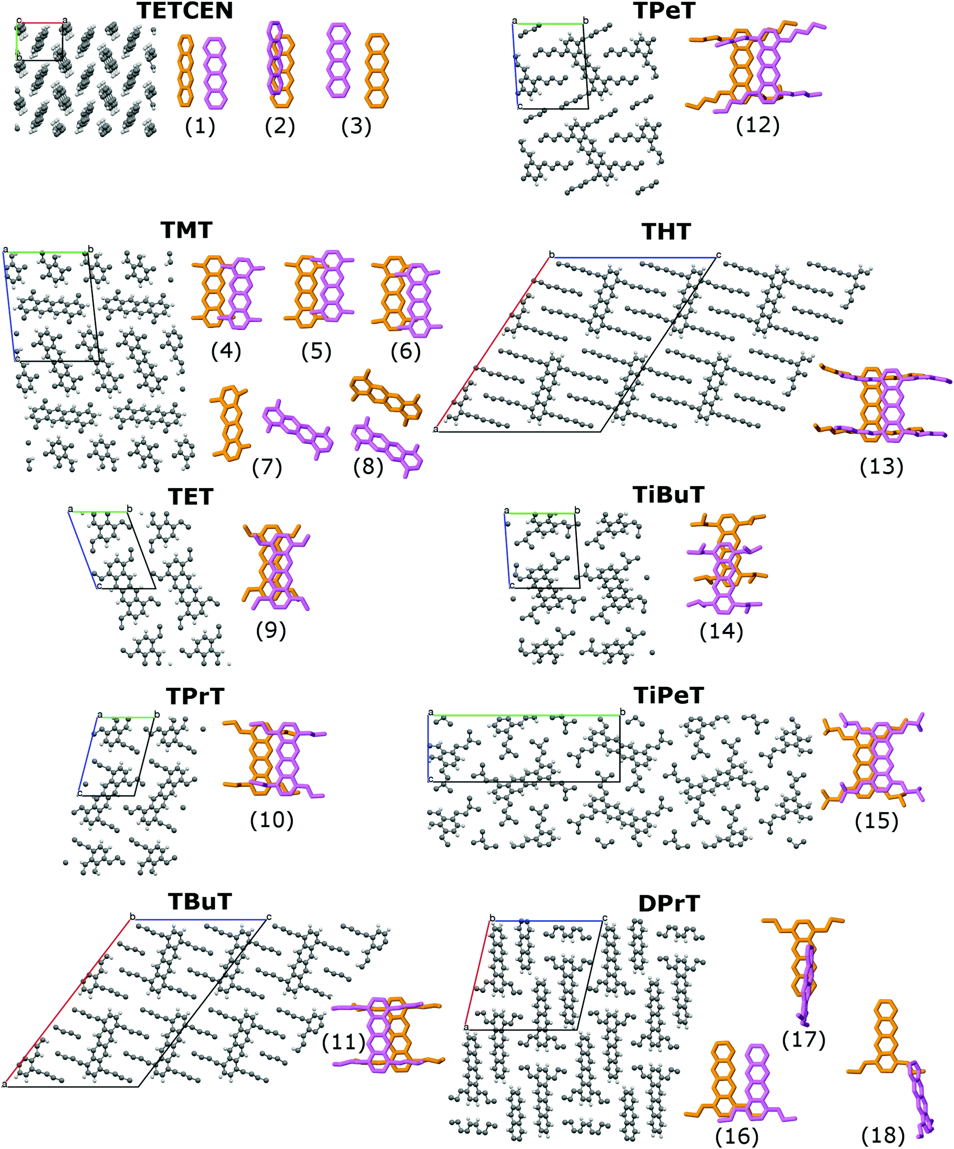 | ||
| Fig. 1 Molecular crystal representations of all systems under study along with each dimer contributing to charge transfer mechanisms. In the case of functionalized tetracenes, the columnar direction is normal to the figure plane. | ||
Initial configurations are based on experimental crystal structures.27,32–34 Every system has been equilibrated by means of periodic molecular dynamics (MD) simulations in the canonical statistical ensemble at room temperature for 1 ns, followed by production MD simulations for 1 ns in the microcanonical statistical ensemble (NVE). From each NVE simulation, a selection of uncorrelated trajectories was singled out, resulting into a swarm of 1024 independent non-adiabatic molecular dynamics simulations per system which were propagated using a nuclear time step of 0.05 fs and an electronic time step of 0.01 fs. Further details are listed in the ESI.†
Methods
Non-adiabatic molecular dynamics (NAMD) simulations by means of the fragment orbital-based surface hopping (FOB-SH) method are utilized in order to examine room temperature polaron dynamics. The key assumptions of the FOB-SH methodology are that the full many-body electronic wavefunction can be replaced by a one-particle wavefunction for the excess charge carrier, with the latter expressed in a quasi-diabatic basis made up of orthogonalized fragment molecular orbitals (FMO), and that electron-nuclei dynamics are approximated by a mixed quantum-classical scheme, with explicit treatment of diagonal and off-diagonal electron–phonon coupling.46–48In the FOB-SH method, an excess charge carrier is treated by a time-dependent one-particle wavefunction Ψ(t) which is expanded on a basis of orthogonalized FMOs:
 | (1) |
![[R with combining right harpoon above (vector)]](https://www.rsc.org/images/entities/i_char_0052_20d1.gif) (t) represent the atomic positions and ϕ the selected FMOs. In the case of electron or hole excess charge carriers, the utilized FMOs are the lowest unoccupied molecular orbitals or the highest occupied molecular orbitals (HOMO), respectively. Following this formulation, the time-dependent Schrödinger equation is expressed as
(t) represent the atomic positions and ϕ the selected FMOs. In the case of electron or hole excess charge carriers, the utilized FMOs are the lowest unoccupied molecular orbitals or the highest occupied molecular orbitals (HOMO), respectively. Following this formulation, the time-dependent Schrödinger equation is expressed as | (2) |
One of the cornerstones of the FOB-SH method is the rapid on-the-fly evaluation of CTIs using the ultrafast analytic overlap method (AOM),50 enabling this way the simulation of extended systems over long time scales. A detailed description of the FOB-SH methodology is included in the ESI.†
The solution of eqn (2) results in the time evolution of the charge carrier wavefunction Ψ(t) which can be used to calculate two crucial quantities: the delocalization of the polaron as described by the inverse participation ratio (IPR) and the charge mobility μ. The former is expressed as
 | (3) |
The charge mobility is calculated via the Einstein relation
| μ = eD/kBT, | (4) |
 | (5) |
 | (6) |
During an FOB-SH simulation, the total force exerted on each atom is calculated as the gradient of the Hamiltonian matrix. According to the AOM, the off-diagonal elements of {Hkl} corresponding to the CTIs are effectively treated as Slater-type orbital (STO) overlap integrals through the Hkl = CSkl scaling law, where C is the system-specific linear scaling constant and Skl the STO overlap values.50 The selection of the sign of the C constant is such as to correctly capture the phase relationships of the CTIs. As a result, the associated force contributions are reduced to gradients of intermolecular STO overlap integrals. The diagonal contributions to the forces are taken from classical force field (FF) expressions. The utilized FF is based on a hybrid all-atom/united-atom representation, with hydrogens explicitly considered only for tetracene cores while the aliphatic side chains are treated at the superatom level of description. This type of FF has been successfully used in the literature for simulating a variety of functionalized PAH molecular crystals.51–53 The accuracy of united-atom FF representations for aliphatic nanophases for molecular crystals made up by soluble molecules with core–shell morphologies has been thoroughly demonstrated in the literature, starting from the early studies of Maliniak54 and Bast and Hentschke55 and leading up to recent implementations for either structural and dynamical properties51,56,57 and charge transfer properties.58–61 Its suitability for MD simulations of tetracene derivatives is confirmed via validation of structural properties with respect to the available experimental information. A complete description of the utilized FF along with further computational details and all validation results are reported in the ESI.†
Moreover, density functional theory (DFT) calculations are carried out for two major purposes: as a preamble for FOB-SH simulations and for independent analyses at the single molecule and dimeric levels of description. As regards single molecule DFT calculations, the so-called 4-point scheme is employed for the determination of hole reorganization energies λ. In the case of molecular dimers, the CTI values are calculated by means of the fragment-orbital DFT (FODFT) methodology62,63 and subsequently scaled as to account for the inherent DFT systematic underestimation as recommended in the benchmark studies of Kubas et al.64,65
All single molecule DFT calculations were carried out using the NWCHEM package.66 Dimeric CTI values by means of the FODFT method were calculated using the CPMD package.67 Relevant technical details are listed in the ESI.† Both classical MD and mixed quantum-classical NAMD simulations were carried out using the CP2K package,68 with the latter utilizing our in-house non-adiabatic MD module.
Results and discussion
When dealing with supramolecular semiconductors, a major indicator regarding charge transfer capabilities and the physical mechanism is the relationship between CTI and the reorganization energy for charge transfer between the neighbouring molecules. An initial differentiation between the possible hopping or band-like polaron diffusion can be achieved by comparing the CTI value along a given direction with the half of the reorganization energy.35 If Hkl > λ/2 then no activation barrier is present, hence leading to carrier delocalization and band-like transfer. On the other hand, if Hkl < λ/2 then an activated hopping charge transfer mechanism is to be expected.In the case of alkylated tetracenes, the side chain length and the morphology appear to have a direct effect on CTIs, since modifications on the peripheral functionalization lead to different crystal structures with distinct intracolumnar stacking patterns. The calculated dimeric AOM CTIs on configurations extracted from MD trajectories along the potential charge transfer pathways in the crystals for all systems under study are plotted in Fig. 2, together with the λ/2 thresholds. The detailed structure for each indexed dimer is depicted in Fig. 1. The reorganization energies for alkylated tetracenes (110–140 meV; see Table 1) are typical for organic semiconductors and an order of magnitude smaller than e.g. for redox processes in aqueous solution69,70 or inorganic oxide materials.71,72
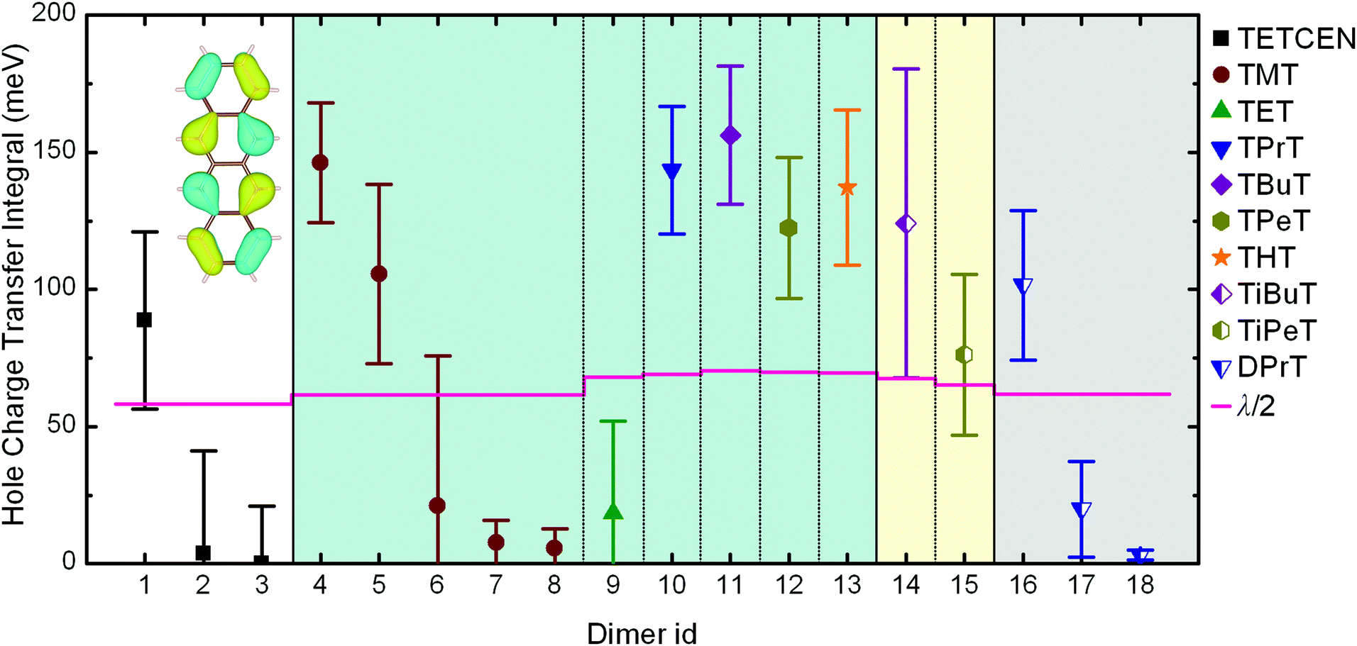 | ||
| Fig. 2 Hole charge transfer integrals for pristine and alkylated tetracene dimers obtained from AOM calculations. Data points and error bars correspond to the mean value and standard deviation of CTIs obtained from equilibrated MD trajectories at 300 K. Each dimer id corresponds to the unique dimeric configurations illustrated in Fig. 1. The horizontal lines correspond to half of the reorganization energy. The inset depicts the HOMO of tetracene. The error bars are calculated from the standard deviation of single Gaussian peaks fitted to CTI values accumulated over room temperature MD simulation results. | ||
| System | λ (meV) | CTIs (meV) | IPR | μ (cm2 V−1 s−1) | μ/μTETCEN |
|---|---|---|---|---|---|
| TETCEN | 116.5 | 88.7 ± 32.4[1]; 3.6 ± 37.5[2]; 0.0 ± 21.0[3] | 3.5 ± 0.02 | 3.5 ± 0.5 | 1.00 |
| TMT | 123.2 | 146.1 ± 21.8[4]; 105.6 ± 32.6[5]; 21.1 ± 54.6[6]; 7.6 ± 8.3[7]; 5.5 ± 7.3[8] | 5.87 ± 0.09 | 20.8 ± 3.2 | 5.9 |
| TET | 136.0 | 18.4 ± 33.6[9] | 1.91 ± 0.01 | 0.6 ± 0.1 | 0.2 |
| TPrT | 138.1 | 143.4 ± 23.3[10] | 5.35 ± 0.05 | 15.8 ± 2.6 | 4.5 |
| TBuT | 140.8 | 156.2 ± 25.2[11] | 5.41 ± 0.06 | 13.2 ± 2.3 | 3.8 |
| TPeT | 139.5 | 122.4 ± 25.7[12] | 4.43 ± 0.05 | 9.6 ± 0.8 | 2.7 |
| THT | 138.9 | 137.1 ± 28.3[13] | 4.74 ± 0.06 | 11.0 ± 1.6 | 3.1 |
| TiBuT | 135.0 | 124.1 ± 56.3[14] | 3.17 ± 0.03 | 1.3 ± 0.5 | 0.4 |
| TiPeT | 130.2 | 76.2 ± 29.4[15] | 3.21 ± 0.03 | 2.7 ± 0.6 | 0.8 |
| DPrT | 123.7 | 101.5 ± 27.3[16]; 19.8 ± 17.5[17]; 3.2 ± 1.9[18] | 5.06 ± 0.12 | 8.2 ± 1.7 | 2.3 |
Pristine tetracene has three dominant CTI values, all belonging to the so-called basal crystal plane. Out of these three, the T-shaped dimer holds the highest value, situated over the λ/2 threshold, suggesting that a band-like diffusion profile should be expected along the direction made up by the tetracene T-dimers. As regards alkylated tetracene derivatives, all of them, with notable exception of TET, feature a pair along the columnar stacking direction where Hkl > λ/2, implying the formation of delocalized polarons and band-like 1D conduction along the stacking direction. In the TMT and DPrT molecular crystals, the type and position of the side chains result in a non-insulating intercolumnar packing, leading to multiple stacking patterns with significant CTI values.
The drastically different crystal packing of alkylated tetracenes compared to their pristine counterpart is shown in Fig. 1: the addition of flexible alkyl side chains effectively breaks the typical herringbone arrangement found in most of the oligoacene crystals, with the layered structure of the pristine tetracene crystal giving way to columnar assemblies. Moreover, in the presence of functional groups, dimer configurations are shifted from T-shaped to parallel-displaced (PD) structures.
An intriguing fact is that the mere side chain length augmentation by one carbon unit – i.e. going from methyl- to ethyl-substituted tetracene – has a significant effect on the dimer structure: the high CTI dimer of TMT (id 4 in Fig. 1) has a clear PD geometry whereas TET adopts a slightly shifted AB-like stacking pattern. This structural difference is carried over to the CTIs, with the value of the TMT dimer being almost eight times larger than that of the CTI of the TET dimer. This radical difference can be readily explained by examining the HOMO overlap between the particular dimers, as shown in Fig. 3. The PD nature of the TMT dimer prompts only constructive orbital superposition, thus leading to high orbital overlap and CTI values; on the other hand, the AB-like stacking pattern of the TET dimer allows for a combination of constructive and deconstructive superposition which results in diminished FMO overlap and CTI values.
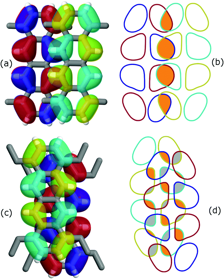 | ||
| Fig. 3 Effect of orbital symmetry on the CTI values for (a and b) TMT and (c and d) TET dimer configurations, corresponding to dimer id 4 and 9 in Fig. 2, respectively. The HOMO isosurfaces for the donor alkylated tetracene molecules are shown in red/blue whereas for the acceptor in cyan/yellow. The right panel illustrates the HOMO overlap for (b) TMT and (d) TET. Orange and grey colored areas correspond to constructive and deconstructive orbital superposition, respectively. Note the large difference in the CTI values, 146 and 18 meV for TMT and TET, respectively, despite a similar stacking distance of 3.6 Å. | ||
In the following we make these initial observations quantitative by explicit propagation of the hole carrier wavefunction in each material followed by calculation of the IPR and the hole mobility. Table 1 contains the aforementioned quantities as obtained from FOB-SH simulation along with the hole reorganization energy and CTI values. The calculated room temperature hole charge carrier mobility for pristine tetracene is equal to 3.5 ± 0.5 cm2 V−1 s−1 and is in good agreement with the experimental reported value of 2.4 cm2 V−1 s−1.21 The highest hole carrier mobility of 20.8 cm2 V−1 s−1 is reported for the TMT molecular crystal, with the associated polaron being delocalized over nearly six tetracene cores inside the conductive molecular nanowire. Similar delocalization profiles are found for all n-alkane substituted tetracenes except TET. The small CTI value of 18.4 meV for the TET dimer, in combination with a reorganization energy of 136.0 meV, results in a poor hole mobility of 0.6 cm2 V−1 s−1, hence rendering this particular system the least attractive candidate for OE charge transfer applications. Moreover, the IPR value of 1.91 is indicative of a charge hopping diffusion mechanism, in striking difference with every other tetracene system examined. The correlation between IPR and the hole mobility values for alkylated tetracenes is shown in Fig. 4, together with two characteristic polaron depictions for the TMT and TET molecular crystals. We found a clear correlation between IPR and the hole mobility, similar to our previous results for unsubstituted oligoacenes.49
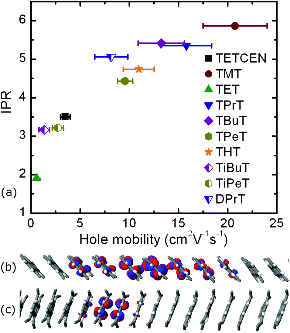 | ||
| Fig. 4 (a) The IPR values with respect to room temperature hole mobility for all systems under study along with detailed illustrations of the polaron spread (b) for TMT and (c) TET. Statistical error bars indicate the standard deviation over four independent blocks of 256 trajectories each. | ||
Iso-alkyl substituted tetracene derivatives constitute an example of the dramatic effect of the side chain type on room temperature mobility. Modification of the linear butyl side chain (TBuT) to a branched iso-butyl side chain (TiBuT) leads to a dramatic decrease in mobility by an order of magnitude and a similar albeit somewhat smaller effect is observed for TiPeT. The utilization of the branched side chains leads to significant intracolumnar stacking pattern variations. As a result, the CTI values are diminished and these two particular systems effectively fail to surpass the barrier of 10 cm2 V−1 s−1 for the hole mobility.
Besides modulating both the room temperature mobility and polaron degree of delocalization, the functionalization profile can practically dictate the spatial characteristics of the charge transfer mechanism. In the alkylated tetracenes discussed so far – i.e. tetra-substituted with n-alkanes (n = 2,…,6) and iso-alkanes – the conductive molecular nanowires are separated in the condensed phase in such a way as to effectively prohibit any intercolumnar charge diffusion, hence forming one-dimensional conduction pathways. This picture is no longer valid for two tetracene derivatives examined here, namely for TMT and DPrT, as it can be clearly deducted via a careful inspection of the reported CTIs in Fig. 2: the aforementioned systems exhibit non-vanishing intercolumnar CTI values, implying that charge transfer pathways between different columns are possible, in addition to the pathway along the columnar direction.
Molecular crystals formed by DPrT molecules exhibit an interesting morphological feature, since the asymmetric functionalization profile with propyl side chains allows the molecular nanowires to come in adequate proximity, enabling this way intercolumnar polaron diffusion. The dynamics of this mechanism is directly mediated by the associated dimeric CTI values. Amongst all the possible dimer combinations in the bulk, DPrT molecules self-organize into three dimer configurations with significant charge transfer potential: the intracolumnar PD dimer with a hole coupling value of 101.5 meV (dimer id 16 in Fig. 1) and two intercolumnar dimers, one T-shaped (dimer id 17 in Fig. 1) and one shifted L-shaped (dimer id 18 in Fig. 1), with CTI values of 19.8 meV and 3.2 meV, respectively.
This gradual cascade in the CTI order of magnitude leads to a special diffusion profile in DPrT molecular crystals: the propagating polaron is primarily situated on a specific molecular nanowire, regulated by the high coupling PD dimer, but can relatively easily migrate onto a neighboring nanowire via diffusive jumps enabled by the intercolumnar T-shaped dimer configuration characterized by the intermediate coupling value of 19.8 meV. This mechanism is inherent to the “twin” DPrT nanowires formed in the solid state which are highlighted as bundles of wires R and G, and B and C shown in Fig. 5. A more infrequent event entails diffusive jumps between the neighboring DPrT nanowires belonging to the adjacent twin bundles, namely the combinations R-C and G-B depicted in Fig. 5. A characteristic propagation profile, as quantified by the time evolution of each wire's cumulative wavefunction expansion coefficients u(t), is shown in Fig. 5. The polaron is initialized on wire B and can propagate through various spatial profiles, i.e. following single wire propagation with short diffusive jumps on the twin wire, crossing to the adjacent wire bundle, or even exhibiting frequent twin diffusive jumps together with infrequent adjacent wire jumps.
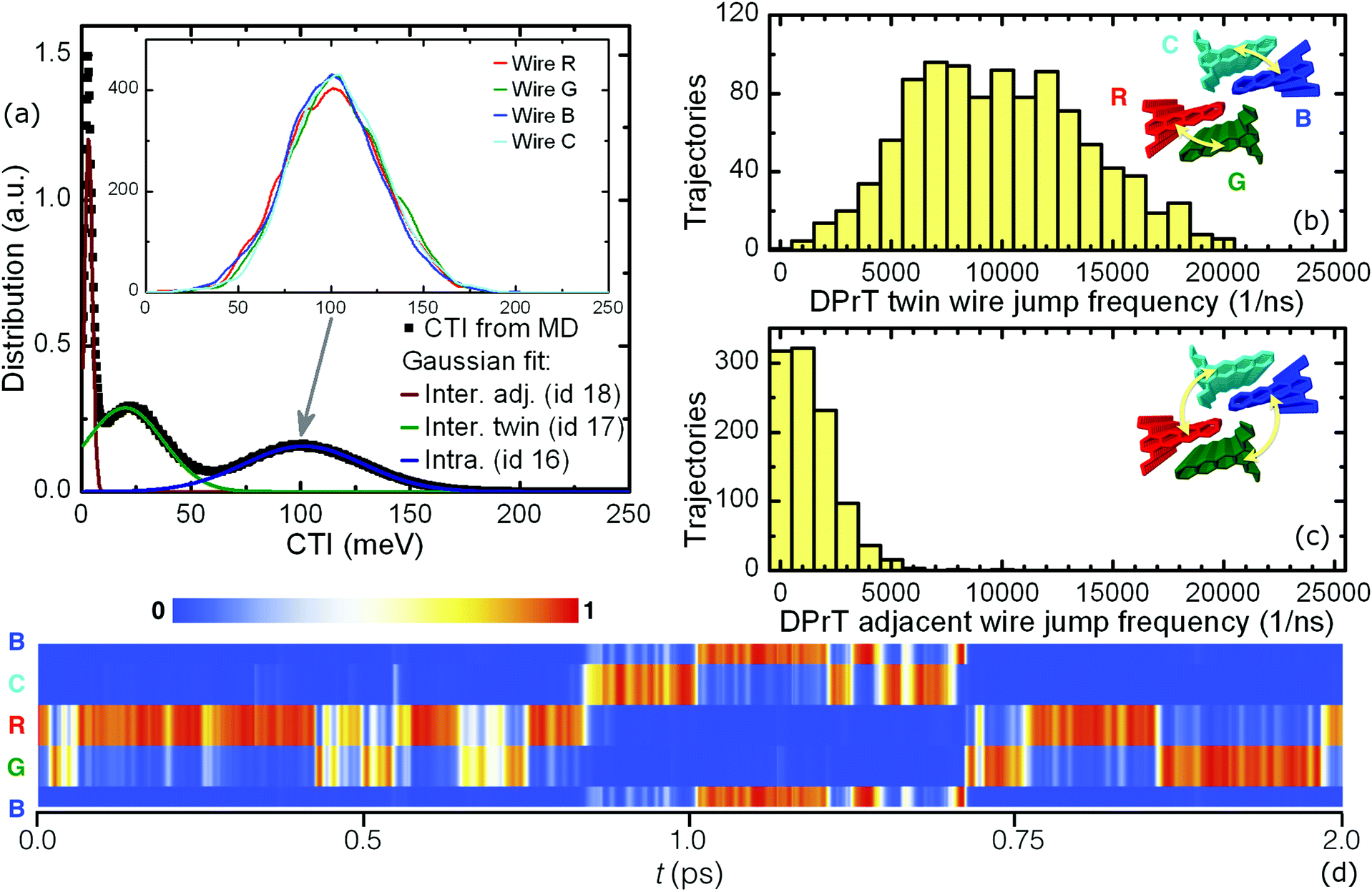 | ||
| Fig. 5 (a) The calculated CTI distribution for the DPrT molecular crystal, with the solid lines corresponding to single Gaussian fit results. The inset depicts the decomposition of the intracolumnar contribution onto the four QM active nanowires embedded in the bulk. (b and c) The statistical profiles of intercolumnar polaron diffusive jumps, with the insets depicting the color-coded QM active pillars: (b) the dominant twin wire jump and (c) the infrequent but present adjacent wire jump. (d) A characteristic polaron propagation profile as quantified by the localization of the time-dependent wavefunction expansion coefficients on each of the four active nanowires. Cyclic periodic boundary conditions apply in the form of the R-G-B-C-R sequence. | ||
A quantification of the polaronic diffusive jumps between the neighboring interacting nanowires in a DPrT molecular crystal is feasible through a statistical analysis of FOB-SH trajectories. A swarm of 1024 statistically independent trajectories was analyzed at equilibrium in order to count the events of intercolumnar diffusion for a duration of 1 ps. In the case of DPrT, the tracked jumps are those of the twin and adjacent wire switch. The histograms describing the frequency of such polaronic jumps are depicted in Fig. 5, along with graphical depictions of the associated wire packings in the insets. The frequent nature of twin wire intercolumnar diffusion in DPrT molecular crystals is evident from the shape of its statistical distribution shown in Fig. 5, suggesting that on average every 100 fs a twin jump occurs. The second mechanism of the adjacent wire jumping encountered in DPrT is less favorable, yet managing to register non-zero counts for up to five events but with a diminished frequency.
A potential issue in a molecular crystal with interacting conductive pillars is the preference between the neighboring molecular nanowires in the bulk. In order to examine if such a behavior occurs, a columnar CTI decomposition is carried out for the DPrT molecular crystal, with the coupling distributions depicted in the inset of Fig. 5a. Due to the fact that DPrT molecular pillars share the same symmetric columnar environment (i.e. every molecular wire has exactly six close contact neighboring wires), no differentiation is present for the CTI values of spatially diverse pillars inside the condensed phase.
The intercolumnar nanowire diffusion profiles in DPrT molecular crystals constitute a mechanism towards robust charge transfer. These easily facilitated twin wire jumps can effectively render the propagating polaron insensitive to local intracolumnar defects such as unfavorable stacking patterns or molecular vacancies. Moreover, even in the case of a bottleneck event on both of the wires belonging to a twin bundle, the excess charge carrier can switch to an adjacent twin bundle. This complex propagation mechanism renders DPrT crystals an excellent candidate for stable quasi one-dimensional conduction with a calculated room temperature hole charge mobility of 8.2 cm2 V−1 s−1.
An intriguing structure–property effect is found for the highest hole mobility system in this study, i.e. the TMT molecular crystal. The methyl substitution forces the molecular pillars to self-organize into a compound two-dimensional lamellar pattern formed by two types of alternating layers along the z crystallographic direction. In one layer type, the nanowires are packed in a brick-like formation with head-to-tail orientation (molecular wires denoted as “V” type in Fig. 6 – since their long axis is vertical to the z direction) whereas in the other layer type, the wires are packed in an edge-to-edge fashion (denoted as “O1” and “O2” in Fig. 6 due to the oblique orientation of the long axis with respect to z).
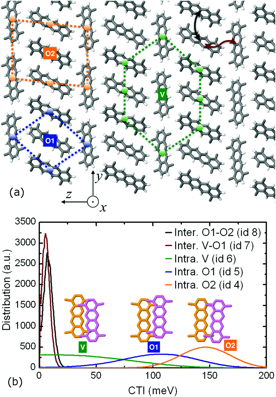 | ||
| Fig. 6 (a) Top view of the TMT molecular crystal, highlighting the three unique pillar types “V”, “O1”, and “O2”, along with their close packing environment. The columnar direction is parallel to the x axis. The two intercolumnar hopping pathways are also shown using arrows. (b) The inter- and intra-columnar distributions of CTI values per molecular wire type, along with intracolumnar dimer representations. | ||
The TMT molecular crystal is the result of the periodic repetition of three types of molecular pillars: “V” wires inside the brick-like lamellae, having eight neighboring pillars in close contact, and “O1” and “O2” types inside the edge-to-edge lamellae, with four and six close contact pillars, respectively. This structural differentiation leads to variable intracolumnar stacking patterns, with the highest coupling value of 146.1 meV belonging to the “O2” pillars, the intermediate CTI value of 105.6 meV attributed to the “O1” pillars and, finally, the smallest value of 21.1 meV to the “V” pillar type. The distribution of both intracolumnar and intercolumnar AOM CTIs is shown in the bottom panel of Fig. 6, along with the insets depicting intracolumnar dimer morphologies.
This inter- and intra-lamellar anisotropy of the hole coupling values gives rise to two intracolumnar transport mechanisms inside the TMT crystal: a “slow”, hopping-like mechanism inside the “V” wires of the brick-type lamellae, with a single column hole mobility of 0.7 cm2 V−1 s−1 and an IPR of 2.3, and two “fast”, delocalized mechanisms, manifested inside the “O1” and “O2” pillars in the edge-to-edge lamellae, with single wire mobilities of 5.6 and 19.1 cm2 V−1 s−1 and IPR values of 3.9 and 5.8, respectively. When all the three columnar types are activated in a FOB-SH simulation, the non-vanishing intercolumnar couplings of 5.5 and 7.6 meV between dimers belonging to “V–O1” and “O1–O2” twin wire bundles prompt diffusive intercolumnar polaronic jumps, with the propagating hole carrier traversing the high coupling “O2” wire, registering a compound quasi-1D mobility of 20.8 cm2 V−1 s−1. This composite transport mechanism that ultimately utilizes the fastest TMT pillar in the bulk is illustrated in Fig. S14 in the ESI,† where the IPR time series are shown for different quantum mechanical (QM) active subregions.
Conclusions
A series of alkylated tetracenes were examined by means of NAMD FOB-SH simulations in order to assess their capabilities as hole conducting media. The tetra-methyl- and tetra-propyl-substituted tetracene derivatives were identified as highly efficient materials for hole transfer, with calculated room temperature mobilities of 20.8 and 15.8 cm2 V−1 s−1, respectively, and a pronounced polaron delocalization over approximately 5–6 molecular units. Our FOB-SH simulations show that the charge carrier propagates through the tetracene cores as a polaron via diffusive jumps, somewhat in analogy with the diffusion of gas molecules in a complex environment,73,74 though with the size and shape of the polaron strongly fluctuating with time.The utilization of flexible side chains drastically alters the molecular self-organization in the solid state, switching from the typical herringbone-like planar arrangement encountered in pristine tetracene crystals to columnar supramolecular complexes. In most of the examined cases, the alkyl nanophase acts as an insulating spacer, practically rendering these materials as true one-dimensional organic semiconductors. The cases of the TMT and DPrT molecular crystals were demonstrated as candidate materials for robust and sizable quasi one-dimensional charge transfer, with the ability of intercolumnar polaron diffusive jumps that can effectively overcome propagation bottlenecks due to local defects.
A clear relationship between the microstructure and charge transport properties is elucidated, proving that the PD stacking patterns along the short molecular axis are directly linked with high mobility tetracene derivatives (systems TMT, TPrT, TBuT, TPeT, THT, and DPrT). The physical interpretation is shown in Fig. 3 and is rationalized through the effect of the stacking motif on the frontier molecular orbital overlap integrals.
Our studies put forward an extended homologous series of alkyl-substituted tetracene derivatives that self-organize into well-defined molecular nanowires and surpass the hole mobility barrier of 10 cm2 V−1 s−1, augmenting this way the “molecular palette” containing promising candidate molecules for efficient flexible OE applications.
Conflicts of interest
There are no conflicts to declare.Acknowledgements
This work was supported by the European Research Council (ERC) under the European Union, Horizon 2020 research and innovation programme (grant agreement no. 682539/SOFTCHARGE) Via our membership of the UK's HEC Materials Chemistry Consortium, which is funded by EPSRC (EP/L000202, EP/R029431), this work used the ARCHER UK National Supercomputing Service (http://www.archer.ac.uk), as well as the UK Materials and Molecular Modeling (MMM) Hub, which is partially funded by EPSRC (EP/P020194), for computational resources. We also acknowledge the use of UCL GRACE and MYRIAD High Performance Computing Facilities.Notes and references
- C. Wang, H. Dong, L. Jiang and W. Hu, Chem. Soc. Rev., 2018, 47, 422–500 RSC.
- X. Zhang, H. Dong and W. Hu, Adv. Mater., 2018, 30, 1801048 CrossRef PubMed.
- C.-F. Liu, X. Liu, W.-Y. Lai and W. Huang, Adv. Mater., 2018, 30, 1802466 CrossRef PubMed.
- D. Ji, T. Li, J. Liu, S. Amirjalayer, M. Zhong, Z.-Y. Zhang, X. Huang, Z. Wei, H. Dong, W. Hu and H. Fuchs, Nat. Commun., 2019, 10, 12 CrossRef PubMed.
- J. E. Anthony, Chem. Rev., 2006, 106, 5028–5048 CrossRef CAS PubMed.
- J. E. Anthony, Angew. Chem., Int. Ed., 2008, 47, 452–483 CrossRef CAS PubMed.
- C. Reese and Z. Bao, Mater. Today, 2007, 10, 20–27 CrossRef CAS.
- S. Allard, M. Forster, B. Souharce, H. Thiem and U. Scherf, Angew. Chem., Int. Ed., 2008, 47, 4070–4098 CrossRef CAS PubMed.
- J. W. Ward, Z. A. Lamport and O. D. Jurchescu, ChemPhysChem, 2015, 16, 1118–1132 CrossRef CAS PubMed.
- B. McDearmon, Z. A. Page, M. L. Chabinyc and C. J. Hawker, J. Mater. Chem. C, 2018, 6, 3564–3572 RSC.
- A. N. Lakshminarayana, A. Ong and C. Chi, J. Mater. Chem. C, 2018, 6, 3551–3563 RSC.
- H. Minemawari, M. Tanaka, S. Tsuzuki, S. Inoue, T. Yamada, R. Kumai, Y. Shimoi and T. Hasegawa, Chem. Mater., 2017, 29, 1245–1254 CrossRef CAS.
- W. Pisula, M. Zorn, J. Y. Chang, K. Müllen and R. Zentel, Macromol. Rapid Commun., 2009, 30, 1179–1202 CrossRef CAS PubMed.
- S. Fratini, S. Ciuchi, D. Mayou, G. T. de Laissardière and A. Troisi, Nat. Mater., 2017, 16, 998–1002 CrossRef CAS PubMed.
- G. Schweicher, G. D'Avino, M. T. Ruggiero, D. J. Harkin, K. Broch, D. Venkateshvaran, G. Liu, A. Richard, C. Ruzié, J. Armstrong, A. R. Kennedy, K. Shankland, K. Takimiya, Y. H. Geerts, J. A. Zeitler, S. Fratini and H. Sirringhaus, Adv. Mater., 2019, 31, 1902407 CrossRef CAS PubMed.
- S. Sergeyev, W. Pisula and Y. H. Geerts, Chem. Soc. Rev., 2007, 36, 1902 RSC.
- H. K. Bisoyi and Q. Li, Prog. Mater. Sci., 2019, 104, 1–52 CrossRef CAS.
- W. Pisula, M. Kastler, D. Wasserfallen, M. Mondeshki, J. Piris, I. Schnell and K. Müllen, Chem. Mater., 2006, 18, 3634–3640 CrossRef CAS.
- H. Cho, S. Lee, N. S. Cho, G. E. Jabbour, J. Kwak, D.-H. Hwang and C. Lee, ACS Appl. Mater. Interfaces, 2013, 5, 3855–3860 CrossRef CAS PubMed.
- D. Nakagawa, C. Nakano, M. Ohmori, H. Itani, Y. Shimizu, A. Fujii and M. Ozaki, Org. Electron., 2017, 44, 67–73 CrossRef CAS.
- C. Reese, W.-J. Chung, M. M. Ling, M. Roberts and Z. Bao, Appl. Phys. Lett., 2006, 89, 202108 CrossRef.
- V. Podzorov, E. Menard, A. Borissov, V. Kiryukhin, J. A. Rogers and M. E. Gershenson, Phys. Rev. Lett., 2004, 93, 086602 CrossRef CAS PubMed.
- W. Xu, Y. He, I. Murtaza, D. Zhang, A. Li, Z. Hu, X. Zeng, Y. Guo, Y. Zhu, M. Liu and H. Meng, J. Mater. Chem. C, 2017, 5, 2852–2858 RSC.
- H. Moon, R. Zeis, E.-J. Borkent, C. Besnard, A. J. Lovinger, T. Siegrist, C. Kloc and Z. Bao, J. Am. Chem. Soc., 2004, 126, 15322–15323 CrossRef CAS PubMed.
- Z. Chen, P. Müller and T. M. Swager, Org. Lett., 2006, 8, 273–276 CrossRef CAS.
- S. Salman, M. C. R. Delgado, V. Coropceanu and J.-L. Brédas, Chem. Mater., 2009, 21, 3593–3601 CrossRef CAS.
- C. Kitamura, A. Takenaka, T. Kawase, T. Kobayashi and H. Naito, Chem. Commun., 2011, 47, 6653 RSC.
- D. Lehnherr and R. R. Tykwinski, Aust. J. Chem., 2011, 64, 919 CrossRef CAS.
- M. Roth, M. Ahles, C. Gawrisch, T. Schwalm, R. Schmechel, C. Melzer, H. vonSeggern and M. Rehahn, Chem. – Eur. J., 2017, 23, 13445–13454 CrossRef CAS PubMed.
- Z. Wang, R. Li, Y. Chen, Y.-Z. Tan, Z. Tu, X. J. Gao, H. Dong, Y. Yi, Y. Zhang, W. Hu, K. Müllen and L. Chen, J. Mater. Chem. C, 2017, 5, 1308–1312 RSC.
- L. Zhang, A. Fonari, Y. Liu, A.-L. M. Hoyt, H. Lee, D. Granger, S. Parkin, T. P. Russell, J. E. Anthony, J.-L. Brédas, V. Coropceanu and A. L. Briseno, J. Am. Chem. Soc., 2014, 136, 9248–9251 CrossRef CAS.
- C. Kitamura, Chem. Rec., 2012, 12, 506–514 CrossRef CAS PubMed.
- C. Kitamura, Y. Abe, T. Ohara, A. Yoneda, T. Kawase, T. Kobayashi, H. Naito and T. Komatsu, Chem. – Eur. J., 2010, 16, 890–898 CrossRef CAS PubMed.
- C. Kitamura, Chemical Science of π-Electron Systems, Springer, Japan, 2015, pp. 69–87 Search PubMed.
- H. Oberhofer, K. Reuter and J. Blumberger, Chem. Rev., 2017, 117, 10319–10357 CrossRef CAS.
- G. Gryn'ova, K.-H. Lin and C. Corminboeuf, J. Am. Chem. Soc., 2018, 140, 16370–16386 CrossRef PubMed.
- I. Yavuz, Phys. Chem. Chem. Phys., 2017, 19, 25819–25828 RSC.
- A. Troisi, Chem. Soc. Rev., 2011, 40, 2347 RSC.
- F. Gajdos, H. Oberhofer, M. Dupuis and J. Blumberger, J. Phys. Chem. Lett., 2013, 4, 1012–1017 CrossRef CAS PubMed.
- H. Yang, F. Gajdos and J. Blumberger, J. Phys. Chem. C, 2017, 121, 7689–7696 CrossRef.
- S. Fratini, D. Mayou and S. Ciuchi, Adv. Funct. Mater., 2016, 26, 2292–2315 CrossRef CAS.
- Y. Jiang, X. Zhong, W. Shi, Q. Peng, H. Geng, Y. Zhao and Z. Shuai, Nanoscale Horiz., 2016, 1, 53–59 RSC.
- C. Liu, K. Huang, W.-T. Park, M. Li, T. Yang, X. Liu, L. Liang, T. Minari and Y.-Y. Noh, Mater. Horiz., 2017, 4, 608–618 RSC.
- J. C. Tully, J. Chem. Phys., 1990, 93, 1061–1071 CrossRef CAS.
- J. C. Tully, J. Chem. Phys., 2012, 137, 22A301 CrossRef PubMed.
- J. Spencer, F. Gajdos and J. Blumberger, J. Chem. Phys., 2016, 145, 064102 CrossRef.
- A. Carof, S. Giannini and J. Blumberger, J. Chem. Phys., 2017, 147, 214113 CrossRef PubMed.
- S. Giannini, A. Carof and J. Blumberger, J. Phys. Chem. Lett., 2018, 9, 3116–3123 CrossRef CAS PubMed.
- S. Giannini, A. Carof, M. Ellis, H. Yang, O. G. Ziogos, S. Ghosh and J. Blumberger, Nat. Commun., 2019, 10, 3843 CrossRef PubMed.
- F. Gajdos, S. Valner, F. Hoffmann, J. Spencer, M. Breuer, A. Kubas, M. Dupuis and J. Blumberger, J. Chem. Theory Comput., 2014, 10, 4653–4660 CrossRef CAS PubMed.
- G. Cinacchi, R. Colle and A. Tani, J. Phys. Chem. B, 2004, 108, 7969–7977 CrossRef CAS.
- O. G. Ziogos and D. N. Theodorou, Mol. Phys., 2015, 113, 2776–2790 CrossRef CAS.
- O. G. Ziogos, S. Konstantinopoulos, L. Tsetseris and D. N. Theodorou, J. Phys. Chem. C, 2018, 122, 18715–18731 CrossRef CAS.
- A. Maliniak, J. Chem. Phys., 1992, 96, 2306–2317 CrossRef CAS.
- T. Bast and R. Hentschke, J. Phys. Chem., 1996, 100, 12162–12171 CrossRef CAS.
- D. Andrienko, V. Marcon and K. Kremer, J. Chem. Phys., 2006, 125, 124902 CrossRef PubMed.
- M. Yoneya, T. Makabe, A. Miyamoto, Y. Shimizu, Y. Miyake, H. Yoshida, A. Fujii and M. Ozaki, Phys. Rev. E: Stat., Nonlinear, Soft Matter Phys., 2014, 89, 062505 CrossRef PubMed.
- J. Kirkpatrick, V. Marcon, J. Nelson, K. Kremer and D. Andrienko, Phys. Rev. Lett., 2007, 98, 227402 CrossRef PubMed.
- V. Marcon, D. W. Breiby, W. Pisula, J. Dahl, J. Kirkpatrick, S. Patwardhan, F. Grozema and D. Andrienko, J. Am. Chem. Soc., 2009, 131, 11426–11432 CrossRef CAS PubMed.
- Y. Olivier, L. Muccioli, V. Lemaur, Y. H. Geerts, C. Zannoni and J. Cornil, J. Phys. Chem. B, 2009, 113, 14102–14111 CrossRef CAS PubMed.
- J. Idé, R. Méreau, L. Ducasse, F. Castet, H. Bock, Y. Olivier, J. Cornil, D. Beljonne, G. D'Avino, O. M. Roscioni, L. Muccioli and C. Zannoni, J. Am. Chem. Soc., 2014, 136, 2911–2920 CrossRef PubMed.
- H. Oberhofer and J. Blumberger, Angew. Chem., Int. Ed., 2010, 49, 3631–3634 CrossRef CAS PubMed.
- H. Oberhofer and J. Blumberger, Phys. Chem. Chem. Phys., 2012, 14, 13846 RSC.
- A. Kubas, F. Hoffmann, A. Heck, H. Oberhofer, M. Elstner and J. Blumberger, J. Chem. Phys., 2014, 140, 104105 CrossRef PubMed.
- A. Kubas, F. Gajdos, A. Heck, H. Oberhofer, M. Elstner and J. Blumberger, Phys. Chem. Chem. Phys., 2015, 17, 14342–14354 RSC.
- M. Valiev, E. Bylaska, N. Govind, K. Kowalski, T. Straatsma, H. V. Dam, D. Wang, J. Nieplocha, E. Apra, T. Windus and W. de Jong, Comput. Phys. Commun., 2010, 181, 1477–1489 CrossRef CAS.
- CPMD version 4.1, The CPMD Consortium, MPI für Festkörperforschung and the IBM Zurich Research Laboratory, 2015, http://www.cpmd.org.
- J. Hutter, M. Iannuzzi, F. Schiffmann and J. VandeVondele, Wiley Interdiscip. Rev.: Comput. Mol. Sci., 2013, 4, 15–25 Search PubMed.
- J. Moens, R. Seidel, P. Geerlings, M. Faubel, B. Winter and J. Blumberger, J. Phys. Chem. B, 2010, 114, 9173–9182 CrossRef CAS PubMed.
- R. Seidel, S. Thürmer, J. Moens, P. Geerlings, J. Blumberger and B. Winter, J. Phys. Chem. B, 2011, 115, 11671–11677 CrossRef CAS PubMed.
- K. P. McKenna and J. Blumberger, Phys. Rev. B: Condens. Matter Mater. Phys., 2012, 86, 245110 CrossRef.
- J. Blumberger and K. P. McKenna, Phys. Chem. Chem. Phys., 2013, 15, 2184 RSC.
- P. Wang, R. B. Best and J. Blumberger, J. Am. Chem. Soc., 2011, 133, 3548–3556 CrossRef CAS PubMed.
- P. Wang and J. Blumberger, Proc. Natl. Acad. Sci. U. S. A., 2012, 109, 6399–6404 CrossRef CAS PubMed.
Footnote |
| † Electronic supplementary information (ESI) available: Description of the FOBSH methodology; systems under study; utilized force field and molecular dynamics simulations details; reorganization energy and charge transfer integral calculations details; classical force field validation results; inverse participation ratio time series for the TMT molecular crystal. See DOI: 10.1039/c9tc05270d |
| This journal is © The Royal Society of Chemistry 2020 |