
 Open Access Article
 This Open Access Article is licensed under a
 Creative Commons Attribution 3.0 Unported Licence
Towards the design of effective multipodal contacts for use in the construction of Langmuir–Blodgett films and molecular junctions†
Enrique
Escorihuela
 ab,
Pilar
Cea
*abc,
Sören
Bock
d,
David C.
Milan
e,
Saman
Naghibi
e,
Henrry M.
Osorio
f,
Richard J.
Nichols
*e,
Paul J.
Low
*d and
Santiago
Martin
*ab
ab,
Pilar
Cea
*abc,
Sören
Bock
d,
David C.
Milan
e,
Saman
Naghibi
e,
Henrry M.
Osorio
f,
Richard J.
Nichols
*e,
Paul J.
Low
*d and
Santiago
Martin
*ab
aDepartamento de Química Física, Facultad de Ciencias, Universidad de Zaragoza, 50009, Spain. E-mail: pilarcea@unizar.es; smartins@unizar.es
bInstituto de Ciencias de Materiales de Aragón (ICMA), Universidad de Zaragoza-CSIC, 50009 Zaragoza, Spain
cInstituto de Nanociencia de Aragón (INA), edificio i + d Campus Rio Ebro, Universidad de Zaragoza, C/Mariano Esquillor, s/n, 50018 Zaragoza, Spain and Laboratorio de Microscopías Avanzadas (LMA), Universidad de Zaragoza, 50018 Zaragoza, Spain
dSchool of Molecular Sciences, University of Western Australia, 35 Stirling Highway, Crawley, WA 6009, Australia. E-mail: paul.low@uwa.edu.au
eDepartment of Chemistry, University of Liverpool, Liverpool, L69 7ZD, UK. E-mail: R.J.Nichols@liverpool.ac.uk
fDepartamento de Física, Escuela Politécnica Nacional, Av. Ladrón de Guevara, E11-253, 170525 Quito, Ecuador
First published on 2nd December 2019
Abstract
As part of on-going efforts to optimize the electrical performance and stability of molecular electronic components, anchor groups that bind molecules to electrode surfaces via multiple points of connection (multipodal contacts) have begun to attract attention. Here an oligo(arylene)ethynylene (OAE) derivative with ‘tripodal’ 2,6-bis((methylthio)methyl)pyridine anchoring groups at both molecular termini has been prepared and used to form well-ordered monolayer Langmuir films at the air–water interface. These films were transferred onto solid supports (surface pressure of transference 8 mN m−1) to give homogeneous, densely packed, monolayer Langmuir–Blodgett (LB) films, which efficiently block a gold electrode surface. Within the surface-supported LB film, the molecules are oriented with a tilt angle of approximately 30° to the surface normal and contacted through both the ‘buttressed’ methylthioether groups and the pyridine nitrogen atom, as determined by X-ray photoelectron spectroscopy (XPS) and shell-isolated nanoparticle-enhanced Raman spectroscopy (SHINERS). Molecular junctions formed by contact of a single molecule within the film by the “STM touch-to-contact” method give a most probable molecular conductance of 4.4 × 10⁻⁵G0. This value compares well with the single molecule conductance of 1,4-bis(pyridin-4-ylethynyl)benzene determined by a variety of methods (3.2–5.4 × 10⁻⁵G0), indicating that the addition of the buttressing groups does not perturb the favourable electrical characteristics of the pyridyl contacting group. Consistent with these conductance data, a transition voltage (Vtrans = 0.48 V) was observed for this ‘buttressed’, pyridine-contacted OAE derivative, indicating relatively good alignment of the metal electrode Fermi level and the frontier molecular orbitals.
Introduction
Molecular electronics uses the electrical properties of molecules located between two or three electrodes to perform some useful function in an electronic device which could potentially offer future technological opportunities.1 Molecular electronic devices have started to appear on the market, for example molecule based components have been incorporated into audio processing circuits.2 Nevertheless, a variety of difficult hurdles must be overcome before a more wide-ranging technological and commercial implementation of molecular electronic devices can be considered.3 In this respect, optimization of the electrical response of molecular junctions is a key milestone. Whilst an immense body of important science has been developed from model single molecule junctions, ‘large area’ ensemble or monolayer film structures are more likely to find implementation in practical device structures.4 With these considerations in mind, studies of molecular junctions formed from well-defined and well-characterized assemblies play an underpinning role in helping to understand the effect of interactions between neighboring molecules within molecular films (e.g. van der Waals forces, π-stacking and polarization effects) on the electrical properties of the junction.5–8Regardless of whether single molecules or assemblies of molecules are used in the construction of molecular junctions, charge transfer through these molecular junctions depends on many complex and often interlinked factors. These include the packing, ordering and number of molecules in the junction, the structure and chemical conformation of the molecular skeleton, the molecular environment including solvent, the metal electrode and the bonding between the anchoring group and these contacts and electric field gradients and electrical potentials, which can arise from bias voltage or electrochemical potential profiles.5,9–12 The importance of the contact-group13 is clearly reflected in the range of contacting groups that have been explored to date, including thiols,14–16 amines,14,17–19 pyridyl,8,20–22 selenols,23,24 nitriles,13,25 isocyanides,26 isothiocyanates,27 dimethylphosphine,28 4-(methylthio)phenyl groups,29 dihydrobenzo[b]thiophenes,30 thienyl rings,31,32 diphenylphosphines,33 trimethylsilylethynyl (TMSE),34,35 and fullerenes.36–38 However, in one way or another, most of these contacts have proven generally to be less than ideal, with complications arising from chemical degradation at operating temperatures,39,40 and associated polymerization phenomena,41 low binding energies,41 high contact resistance42–47 or variability in the binding geometries leading to multiple conductance values for a given molecule.48–53
In efforts to create more robust and well-defined molecule-to-electrode contacts, attention has been turned to surface binding systems in which contact to the surface is made through more than one atom in the anchor group; examples of such systems include pyrazolyl,54 bis(terpyridine),55 carboxylates,14,37,56,57 dithiocarbamates58,59 or carbodithioates.60,61 Alternative anchoring strategies based on the use of multiple individual contacting groups have also been conceived and investigated, including bidentate dithiols,62–64 diols (catechol),65 and norbornyldithiol,66,67 and a wide variety of molecular ‘caltrops’.68–70 In many cases, these systems have been used to promote the formation of single-molecular junctions and the electrical properties of such systems have been investigated.66,67,71–76 In certain cases these junctions can show fewer fluctuations due to stronger, and hence more stable, linkages to the substrate.77–79
Despite these attractive properties, the development of ‘large area’ junctions formed by molecular assemblies of multipodal platforms and the determination of the electrical properties of these systems has received relatively little consideration to date,68,80–82 being complicated at least in part by the challenges of matching the registry of surface anchor points with the molecular spacing and positioning imposed by the constraints of the film structure. In this paper we report the synthesis and the Langmuir and Langmuir–Blodgett (LB) film forming behaviour of a 1,4-bis(pyridylethynyl) benzene8,83 derivative, in which the electrical contact through the pyridyl moiety is augmented by the introduction of ‘buttressed’ methyl(thiomethyl) anchors (1) (Fig. 1). Whilst the pyridyl groups can form N–Au σ-contacts and π-contacts between the pyridyl face and adatom or defect features on the electrode surface,20,84 the buttressing methylthioether groups provide additional strong S→Au interactions, enhancing the physical contact between the molecule and electrode surface. However, these buttresses are electronically decoupled from the molecular core by the methylene (CH2) linker to reduce complications arising from additional electron transfer pathways and associated quantum interference (QI) effects.85 Together, the thioether and pyridyl moieties have the potential to create a robust platform through which the ‘electrical’ contact (pyridyl) is reinforced by methylthioether ‘buttresses’ which enhance the adhesion of the molecule to the electrode surface. This combination of contacting groups, each of which can interact with a putative (gold) electrode surface, allows the interplay between the enhanced physical molecule–surface contact and molecular conductance to be explored within a monolayer film.82,86
 | ||
| Fig. 1 A sketch of molecule 1, illustrating the buttressing methyl(thiomethyl) groups around the pyridyl-based anchor points. | ||
Results and discussion
Assembly of Langmuir and Langmuir–Blodgett (LB) films
A preliminary survey was undertaken to assess the influence of the concentration and volume of the spreading solution on the formation of Langmuir films of 1 at the air–water interface. This survey concluded that only solutions with a concentration lower than 1 × 10⁻⁵ M, yielding initial surface densities less than 8.3 × 10⁻¹¹ mol cm−2 produced surface pressure vs. area per molecule (π–A) isotherm reproducibly (Fig. 2). Under these conditions, the isotherm shows (left-hand axis) a gas phase region from 1.80 to 0.90 nm2 molecule−1, which is recognized by its vanishing surface pressure. At 0.90 nm2 molecule−1, a sharp increase of the π–A isotherm occurs, which is followed by a rather steady increase of the surface pressure upon further compression up to 0.35 nm2 molecule−1 where the change in the slope indicates the transition of the monolayer to a more condensed phase. Fig. 2 also shows (right-hand axis) the normalized surface potential, ΔVn (surface potential multiplied by the area per molecule), versus area per molecule isotherm.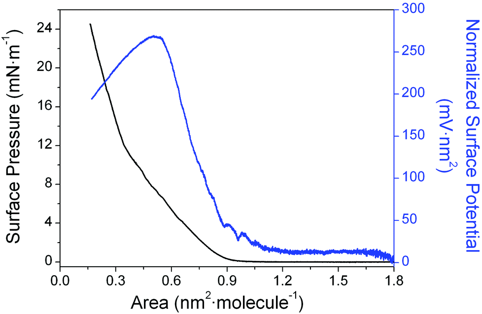 | ||
| Fig. 2 Surface pressure (π–A) and normalized surface potential (ΔVn–A) vs. area per molecule isotherm of 1. | ||
Normalized surface potential data typically give useful information about ordering of molecules within the monolayer. For monolayers of 1 with the area per molecule greater than 0.90 nm2 molecule−1, fluctuations in the surface potential were found to occur, probably due to the formation of small domains within a predominantly gas phase monolayer. As these domains coalesce to more condensed phases, a region without fluctuations where the normalized surface potential increases almost linearly is observed (0.90–0.55 nm2 molecule−1). This is likely due, at least in part, to the increasing order that maximizes attractive intermolecular forces (e.g. π–π interactions) between the neighbouring molecules of 1 upon compression, even in the (pseudo) gas phase region of the isotherm. This increased order might be expected to lead to increasing hydrophobicity of the local environment of the molecules, and to a localized decrease in the dielectric constant associated with the region of the head group.87 These deductions are in-line with the experimentally observed rise in the normalized surface potential upon compression to 0.55 nm2 molecule−1. A change in the gradient of the surface pressure response at ca. 0.55 nm2 molecule−1 is then attributed to an evolution to a more condensed phase. An almost flat region of the normalized surface potential response from 0.55 to 0.48 nm2 molecule−1, with minor variation ascribed mainly to the reorientation of the sulfur groups and the water molecules at the interface follows. Finally, the local collapse of the monolayer occurs with dipole moments then being randomly arranged. This manifests itself by the precipitous decrease in ΔVn at areas per molecule less than 0.48 nm2 molecule−1.
The effect of changes in surface pressure on the molecular organization of 1 within the Langmuir films was further examined by in situ UV-vis reflection spectroscopy. Spectra were recorded under normal incidence with unpolarised light (Fig. 3). The intensity of the band at 325 nm, characteristic of the π-conjugated backbone of the oligo(arylene ethynylene) (OAE) moiety,88 decreases considerably upon compression. This observation points to a steady decrease of the tilt angle between the main molecular axis and the surface normal. In other words, upon compression the transition dipole moment of the molecule (which is directed along the main molecular axis) progressively moves to a more upright orientation with respect to the water surface.89 The appearance of the π–π* band in the films of 1 at the same transition energy (wavelength) as 1 in solution suggests that the formation at the interface of bidimensional (2D) aggregates is suppressed under these conditions.6–8,90–92
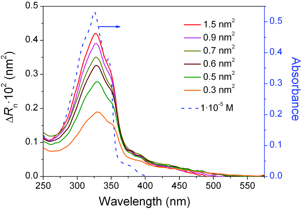 | ||
| Fig. 3 Normalized reflection spectra, ΔRn (= ΔR area per molecule) of a Langmuir film of 1, recorded at six different values of compression as indicated by the areas per molecule (solid lines and left axis). A UV-vis absorption spectrum of a 1 × 10⁻⁵ M solution of 1 is included for comparison (blue dashed line and right axis). | ||
These high-quality Langmuir films were transferred onto solid supports to give the substrate supported Langmuir–Blodgett (LB) films. This was achieved using the vertical dipping method with the substrate initially immersed in the subphase. Monolayers of 1 were deposited at different surface pressures onto mica substrates, which had been freshly cleaved, and the resulting LB films were imaged using an atomic force microscope (AFM) (Fig. 4). The films transferred at a surface pressure of 15 mN m−1 displayed an inhomogeneous structure with multilayer regions and a root mean square (RMS) surface roughness of 1.23 nm. Films transferred at 10 mN m−1 (RMS 0.30 nm) were more uniform, but the images revealed small regions of localized collapse of the monolayer and three-dimensional defects. In contrast, films transferred at 5 mN m−1 were free of such 3D defects, but also failed to uniformly cover the substrate leading to holes in the monolayer (RMS 0.26 nm). The optimal surface pressure of transference was therefore determined to be 8 mN m−1 (RMS 0.21 nm), giving uniform monolayer LB films largely free of perforations and 3-dimensional defects. An LB film was also transferred to a gold substrate at 8 mN m−1, and examination of the surface by AFM corroborated the formation of a uniform monolayer largely free of perforations or holes and 3-dimensional defects at this surface pressure on this substrate material (Fig. S1, ESI†).
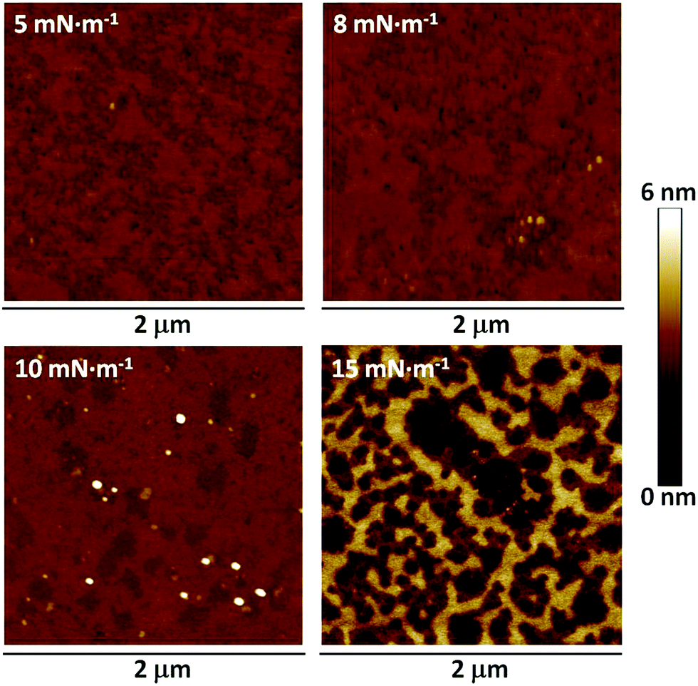 | ||
| Fig. 4 Atomic force microscopy images of a LB monolayer of 1 transferred to mica at the surface pressures indicated. | ||
To complement the isotherm and AFM imaging data, the defect density in the film was evaluated indirectly by comparing the electrochemical response of K3[Fe(CN)6] (as a 1 mM solution in 0.1 M KCl aqueous solution) at a pristine gold working electrode and at a gold electrode surface modified by a high quality LB film of 1 formed at 8 mN m−1.93 As expected, the cyclic voltammetric response of the pristine gold electrode shows a clear voltammetric wave for the ferricyanide redox probe. On the other hand, in the case of the LB monolayer modified electrode, the current signal is almost totally suppressed (Fig. 5). This corresponds to effective blocking of the electrode by the monolayer LB film and the response is consistent with a low density of perforations or defects in the organic film, in agreement with the AFM observations (Fig. 4, Fig. S1, ESI†).
 | ||
| Fig. 5 Cyclic voltammograms of aqueous 0.1 M KCl solutions containing 1 mM K3[Fe(CN)6] recorded at a scan rate of 0.1 V s−1, at either a bare gold working electrode (black curve) or a monolayer film of 1 on gold formed by the LB method at 8 mN m−1 (blue curve). A Ag|AgCl|satd KCl reference electrode was deployed alongside a Pt sheet counter electrode to complete the three-electrode cell configuration. | ||
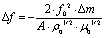
The surface coverage of the monolayer was quantitatively determined using a quartz crystal microbalance (QCM) resonator. Here the change in the resonator frequency (Δf) was determined before and after the LB film formation process. The Sauerbrey equation was then applied to determine the corresponding mass change and from this the surface coverage was obtained:94
 | (1) |
The UV-vis absorbance spectrum of a LB monolayer of 1 transferred at 8 mN m−1 onto the quartz substrate was also recorded to gain further details concerning the molecular organization of 1 in the LB film. The spectrum displays a broadly similar shape to the reflection spectra obtained at the air–water interface at the same surface pressure with an absorption peak at 325 nm, but with lower apparent molar absorptivity (Fig. 6). This points to either a reorientation of the molecules to a more upright orientation with respect to the substrate during the transference process or to the scattering background in the Langmuir film that is not present in the LB film.
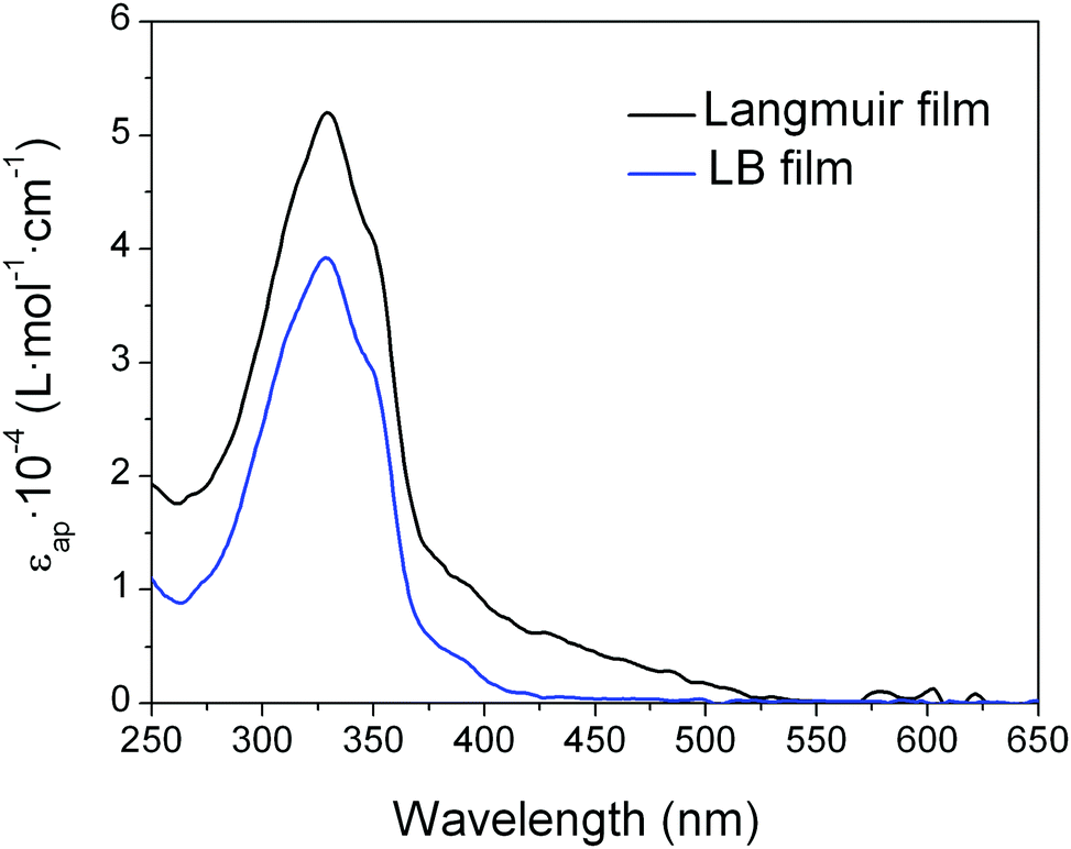 | ||
| Fig. 6 Apparent molar absorptivity (εap) for a Langmuir film and a LB film of 1 at a surface pressure of 8 mN m−1. | ||
With the conditions leading to well-ordered and tightly packed LB monolayers of 1 established, attention was turned to X-ray photoelectron spectroscopy (XPS) and shell-isolated nanoparticle-enhanced Raman spectroscopy (SHINERS) to provide insight into the binding interactions between 1 and the gold substrate via the various potential contacting groups. The XPS data for the N1s region from the powder sample of 1 (Fig. 7) contain a single peak at 398.3 eV arising from the (identical) N atoms of the pyridyl groups.95 In contrast, the XPS spectrum of the LB film of 1 on gold displays two distinct N1s peaks (Fig. 7b). The peak at 398.3 eV is consistent with the powder measurement of 1 and indicates that in the film some of the pyridine moieties are non-bonded and free of the gold surface. A second peak at higher binding energy (399.3 eV) is attributed to the N atoms of pyridyl moieties chemisorbed on gold96 and provides important evidence for the interaction of the pyridine ‘electrical’ contact in the multipodal anchor to the electrode surface.
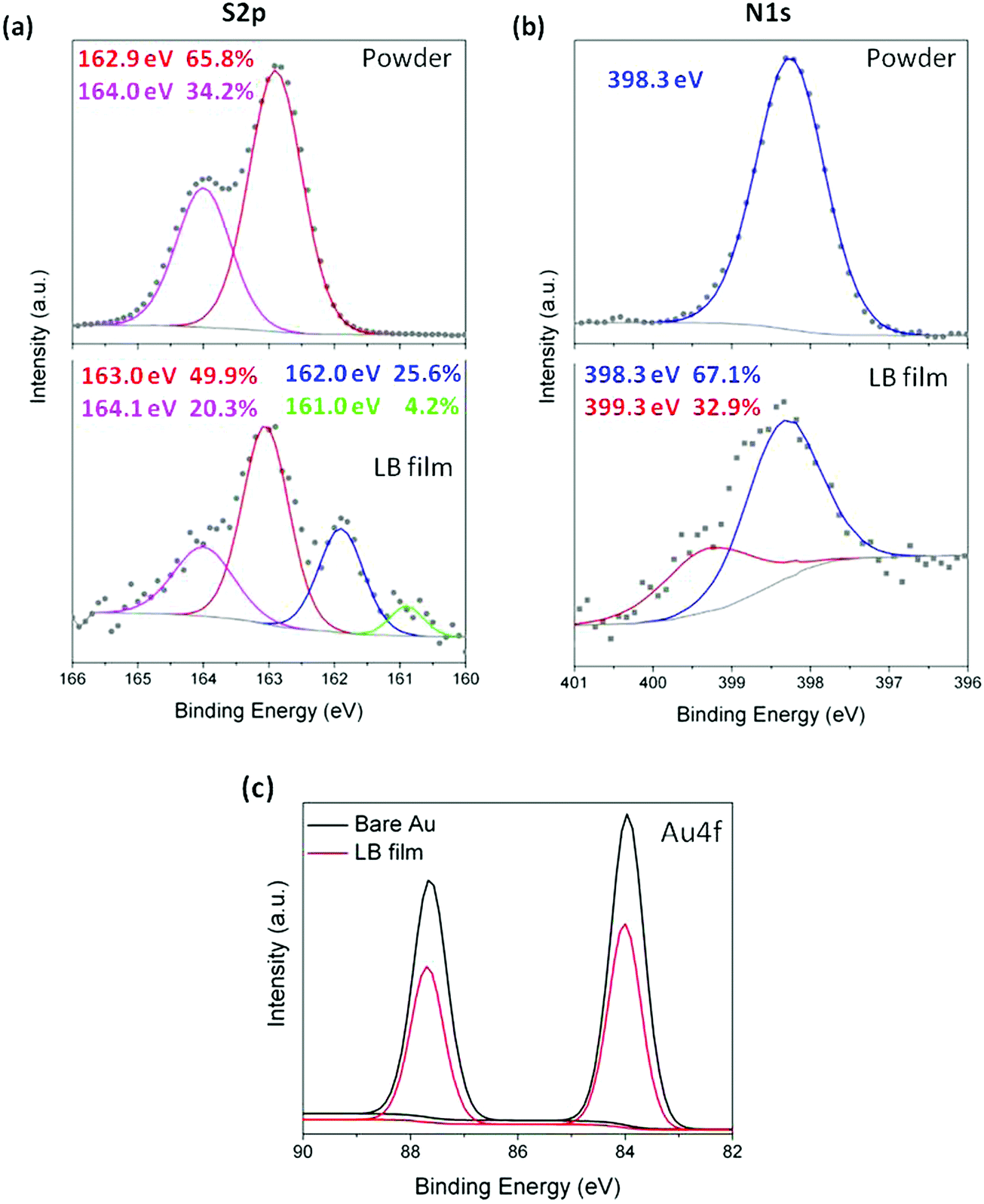 | ||
| Fig. 7 XPS spectra recorded in the (a) S2p and (b) N1s regions for 1 in powder form and in a LB film transferred at 8 mN m−1. The grey close circles are the experimental spectra and the coloured lines are the deconvoluted fits. (c) XPS spectra of the Au4f region for an uncovered Au substrate and a Au substrate covered by a LB film of 1. | ||
On the other hand, to evince interactions between buttressing thioether moieties and the gold substrate, XPS was also used. As a consequence of spin–orbit splitting effects,97,98 the XPS spectrum of a powder sample of 1 in the S2p region (Fig. 7a) displays two peaks with an area ratio of 2![[thin space (1/6-em)]](https://www.rsc.org/images/entities/char_2009.gif) :1 (65.8% and 34.2%) at 162.9 and 164.0 eV (peak separation of 1.1 eV) assigned to (2p3/2) and (2p1/2), respectively. The XPS data from an LB film of 1 transferred at a surface pressure of 8 mN m−1 onto a gold substrate are more convoluted. The most intense pair of S2p peaks at 163.0 and 164.1 eV appear at practically the same binding energy as those observed for the powder sample of 1, and indicate that at least some of the methylthioether moieties in 1 are free from bonding interactions with the gold substrate supporting the monolayer. At lower binding energy, two attenuated S 2p3/2 peaks arising from S atoms in different contact modes with the gold substrate are observed at 162 eV and 161 eV,82,99 the corresponding weaker 2p1/2 peaks would be expected to fall ca. 1.2 eV higher in energy (i.e. at 163.2 eV and 162.2 eV, respectively) being obscured by the more intense peaks from the methylthioether moieties not attached to the surface.
:1 (65.8% and 34.2%) at 162.9 and 164.0 eV (peak separation of 1.1 eV) assigned to (2p3/2) and (2p1/2), respectively. The XPS data from an LB film of 1 transferred at a surface pressure of 8 mN m−1 onto a gold substrate are more convoluted. The most intense pair of S2p peaks at 163.0 and 164.1 eV appear at practically the same binding energy as those observed for the powder sample of 1, and indicate that at least some of the methylthioether moieties in 1 are free from bonding interactions with the gold substrate supporting the monolayer. At lower binding energy, two attenuated S 2p3/2 peaks arising from S atoms in different contact modes with the gold substrate are observed at 162 eV and 161 eV,82,99 the corresponding weaker 2p1/2 peaks would be expected to fall ca. 1.2 eV higher in energy (i.e. at 163.2 eV and 162.2 eV, respectively) being obscured by the more intense peaks from the methylthioether moieties not attached to the surface.
To further evince the interaction between methylthioether moieties and the gold substrate, SHINERS was used to record the Raman spectrum of films of 1 on gold. In this spectrum a band is seen at 400 cm−1, which is unique to the film of 1 on gold (Fig. S3, ESI†). This can be attributed to the ν(Au–S(R)) modes arising from the contact between the thioether moieties and the gold surface in different contact geometries.100,101 To support this assignment we note that a SAM of thioanisole (i.e. (methylsulfanyl)benzene) on gold displays a unique ν(Au–S(Me)) band at ca. 380 cm−1 that is not present in the spectrum of the pure compound, or in the SAMs of thioanisole on glass (Fig. S4, ESI†).
Taken as a whole, the data presented above indicate that in the LB film, molecules of 1 are oriented rather normal to the substrate surface and contacted the solid substrate through one of the pyridine groups with additional interactions through some of the methylthioether moieties of 1. Given that each S2p3/2,1/2 doublet has a branching ratio of 2:1 (S2p3/2/S2p1/2), based on the relative intensities of the clearly observed peaks at 164.1 eV (non-bonded SMe, S2p3/2) and 161.0 eV (bound SMe, S2p1/2) one can estimate that the corresponding areas associated with each signal in the convoluted spectrum should be: 20.3% (164.1 eV), ∼41% (163 eV), ∼11% (∼163.2 eV), ∼23% (162.0 eV), ∼2% (162.2 eV) and 4.2% (161.0 eV). That is, the relative area of XPS signals arising from sulfur atoms in the film of 1 bound in the various contact geometries and non-bonded to the gold substrate is approximately 39:61. An estimate of the relative proportions of sulfur in these bound vs. non-bonded states was made on the basis of the attenuation of the Au4f XPS signal from the gold substrate covered by a LB film of 1 (Fig. 7c), given the broadly similar binding energies of Au4f and S2p, and taking into account the exposed areas of gold that are not covered by the LB film (4.2%) according to the bearing analysis made in the AFM image (Fig. S2, ESI†) an attenuation factor of 0.64 was obtained. Thus, an equal number of bound and non-bonded sulfur atoms in the film of 1 on gold would be expected to give rise to XPS signals in an approximate ratio of 40:60, very close to the integrated areas of the peaks observed in the experimental spectra. The combined weight of evidence drawn from the studies described above indicates that in the film, molecules of 1 come into contact with the gold substrate through the N lone pair to the gold surface, reinforced with additional interactions through the two buttressing methylthio ether moieties with various surface binding sites on the substrate in a 1:1 ratio of bound to non-bonded methylthio ether and pyridyl moieties. The opposite ‘multidentate’ moiety is then exposed on the top surface of the film and thereby available to contact a top electrode (Fig. S5, ESI†).
This proposed model of contact for the methylthioether buttressed compound 1 can be compared to results from a recent investigation of Sander on a series of structurally similar buttressed pyridine-2,6-diyldi(methanethiol) compounds, such as can be derived from the acyl-protected derivative 2 (Fig. S6, ESI†).82 In self-assembled (SA) films, the thiolate derivatives of 2 do not bind homogeneously with strictly bidentate contacts to the surface despite the strength of the thiol–gold bond. Probably, as a consequence of the packing demands in the SAM, these compounds bind asymmetrically with one sulfur anchor entering into thiolate-type binding with the gold substrate, whilst the other is weakly coordinated, not bonded (likely as the thiol) or involved in a disulfide bond with an adjacent molecule. The synchrotron HRXPS N1s spectrum of a film of 2 exhibits a peak at a binding energy close to 398.7 eV, consistent with the pyridine N atom being non-bonded at the gold surface (which would give a peak nearer 400 eV). Therefore, in the case of SA films of 2, the contact between the pyridyl ring and the gold surface is thought to be more through the pyridyl π* system than the N lone pair.82
The proposed models of binding for 1 (Fig. S5, ESI†) and 2 (Fig. S6, ESI†) are distinguished by the proposed N–Au contacts supported by the SMe buttresses in 1 (Fig. S5, ESI†) and the more prominent surface-(pyridine π*) interactions proposed for self-assembled films derived from 2 (Fig. S6, ESI†). The Au–π* contacts are thought to be responsible for the higher conductance features observed in the I–s traces at smaller electrode separations, whilst at greater electrode separations that correspond more closely to the molecular length (as defined by the N⋯N distance between the pyridyl contacts at each end of the molecule) the molecule slides into a conformation where the contacts to the electrodes are made through the N-atoms.20 This suggests that molecular conductance measurements may also provide some further information related to the putative pyridine(N)→Au(surface) interaction.
The electrical characteristics of a LB film of 1 formed on Au(111) substrates were recorded using a variation of the STM current–distance (I(s)) method initially developed by Haiss and co-workers.102 In brief, the I(s) technique involves using the STM tip to form Au(substrate)|molecule|Au(tip) molecular junctions from dilute solutions of the analyte in a STM liquid cell formed on a conductive substrate. Alternatively the conductive substrate may be initially modified with a sub-monolayer of the analyte. In either case the STM tip is allowed to approach, but not touch, the substrate. The STM tip is then withdrawn away from the substrate and the current recorded as the tip–substrate separation is increased. If no molecules under study are caught between the tip and substrate, plots of current vs. distance show a typical exponential decay associated with tunnelling through the solvent or air gap between the tip and substrate. In contrast, when a molecular junction is formed by an analyte molecule bridging between the STM tip and substrate, characteristic plateaus in the current–distance (I(s)) scans are observed, which can evolve as the molecular geometry rearranges to accommodate the increasing electrode separation. At some point the electrode separation exceeds the span of the molecule, causing the junction to abruptly break and a rapid decay in the current. The junction making and breaking process is repeated many times by continually approaching and retracting the STM tip and the current data are compiled into conductance histograms which reveal peaks corresponding to the most probable molecular conductance values.
The “STM touch-to-contact” method is an adaptation of the I(s) method, suited for the formation of single-molecule junctions from monolayer films.86 This approach to the measurement of molecular conductance within monolayer films is rather different to using liquid eutectics of gallium and indium98–105 as top contact electrodes or conducting AFM106–111 and other ‘large-area’ junction methods, where a relatively large number of molecules within the film are contacted. In these cases it is necessary to know the contact area and the surface coverage to infer single molecule properties, while these parameters are not needed for single molecule contacts made with the “STM touch-to-contact” method. Here, an electrochemically etched and atomically sharp STM tip is positioned so as to just touch the top surface of a molecular monolayer. Incursion of the tip into the monolayer is avoided, so as to leave the arrangement of molecules within the monolayer unperturbed. Conductance values obtained using this method are in excellent agreement with ‘conventional’ single-molecule junctions formed from low coverage molecular films and the I(s) technique as reported previously.6–8,90 Thus, in contrast to ‘large area’ monolayer film sandwich devices formed with macroscopic ‘top’ electrodes, the atomically sharp tip used in the “STM touch-to-contact” method permits the formation of single-molecule junctions with individual molecules within substrate-supported monolayers.
In order to locate the STM tip on top of the LB film, which is a requirement of the “STM touch-to-contact” method, the LB film thickness needs to be quantified by an independent method, followed by a calibration of the tip–substrate separation. The thickness of the monolayer (1.80 nm) was obtained through analysis of the attenuation of the Au4f signal in the XPS spectra (Fig. 7c) as described in the Experimental Section. To corroborate this thickness, a height profile using a defect in an AFM image of a LB film of 1 transferred at 8 mN m−1 onto mica was made. A height of 1.9 nm was obtained, in perfect agreement with that determined by XPS (Fig. S7, ESI†). A layer thickness of 1.8 nm corresponds to an inclination angle with respect to the surface normal of ∼30° according to the molecular length (determined by molecular modelling using the Spartan suite of programs, 2.04 nm). This reveals that an interaction between the nitrogen at the bottom contact and the gold substrate may exist alongside the surface bonding through two methylthiol groups. This ties in with the deductions from XPS and SHINERS, and is remarkably close to the value determined from the films of pyridine-2,6-diyldi(methanethiol) (24 ± 3°).82
Calibration of the tip–substrate distance (s) was achieved by transforming the set-point parameters (set-point current, I0, and tip bias, Ut) into an absolute gap separation (s) as follows. A series of current–distance retraction scans (I(s) curves) which showed a plain exponential decay of the tunnelling current were recorded at regular times and at different substrate locations during the measurements. Such plain exponential decay curves correspond to situations where molecules do not bridge (“wire”) between the STM tip and substrate. These curves were recorded with set-point parameters of I0 = 60 nA and Ut = 0.6 V to ensure that the STM tip is pushed into the LB film before the retraction. These I(s) curves were used to quantitatively estimate the current decay dlnI/ds within the LB film by plotting lnI versus s. Note that there is typically a curved region at the beginning of the lnI vs. s retraction scan which arises from an initial inertia in the piezo movement and this is omitted from the analysis. Slopes of 5.1 ± 0.9 nm−1 were obtained and this value aligns well with decay values for comparable conjugated compounds within molecular films.6–8,92 From this, current and voltage set-point values to then locate the STM tip touching the top of the LB film can be estimated (eqn (2)). To achieve this it is necessary to use the dln(I)/ds value estimated for the LB film and to also estimate the current when the STM tip would hypothetically just atomically touch the gold substrate. The latter is taken as the “point contact” or G0 (where G0 = 2e2/h = 77.5 μS) conductance of gold. The following equation is then used to calculate the absolute tip–gold substrate separation and to adjust it such that the STM tip just touches the top of the monolayer:
 | (2) |
lnI/ds = 5.1 nm−1 and set-point parameters of I0 = 5.2 nA and Ut = 0.6 V a tip–substrate distance estimation of 1.80 nm is obtained, in good agreement with the thickness of the monolayer determined independently by XPS. Therefore using these set-point parameters, current–voltage (I–V) curves can be recorded with the tip just in contact with the top of the monolayer LB film. Fig. 8a shows the average I–V curve recorded using these touch-to-contact conditions (I0 = 5.2 nA and Ut = 0.6 V) for a LB film transferred onto Au(111) at a surface pressure of 8 mN m−1. This curve was averaged from 420 I–V curves recorded from different locations and various substrates. As seen in Fig. 8a there is a characteristic curvature over the bias window from −1.2 V to +1.2 V and the curve is symmetrical around zero bias. From the low-voltage region (from −0.2 to +0.2 V), where the I–V curve is approximately linear (Ohmic), a conductance value of 4.4 × 10⁻⁵G0 is obtained. Crucially, this value is in excellent agreement with that previously determined for the ‘parent’ 1,4-bis(pyridin-4-ylethynyl)benzene (3.2–5.4 × 10⁻⁵G0) using the “STM touch-to-contact” method,8 the I(s) technique8 or mechanically controlled break junctions83 contacted through the pyridyl N atoms.
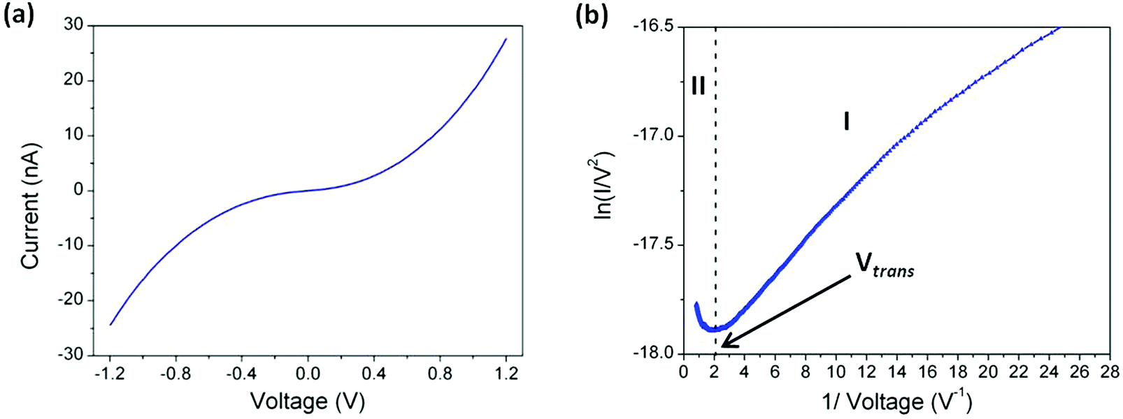 | ||
| Fig. 8 (a) I–V curve averaged from 420 individual traces. Data recorded for an LB film of 1 transferred onto Au(111) at a surface pressure of 8 mN m−1 using as set-point parameters I0 = 2.8 nA and Ut = 0.6 V. (b) Fowler–Nordheim plot for the 1I–V curve, where two distinct regimes (I and II) are evident. | ||
In order to obtain a further analysis of the electrical properties of 1, a Fowler–Nordheim (eqn (3)) plot was obtained (Fig. 8b).
 | (3) |
In the low-bias region I marked in Fig. 8b ln(I/V2) shows growth with ln(1/V), which points to direct tunnelling. On the other hand, region II exhibits a negative slope, with ln(I/V2) linearly scaling with 1/V and this behaviour corresponds to field emission (eqn (3)). This transition point between regions I and II is called the transition voltage, Vtrans. This has been shown to be linearly correlated with, but not directly equal to, the energy difference between the frontier molecular orbital level and the metal Fermi level.103 The Vtrans value, 0.48 V, is significantly lower than values obtained for comparative phenylene–ethynylene derivatives contacting metal surfaces through monodentate platforms formed by typical electrode-contacting groups such as thiol, amine or carboxylic acid,103–106 suggesting the merits of pyridyl-based contacts in the design of OAE-based molecular components.
Conclusions
In this paper, an oligo(arylene)ethynylene (OAE) derivative with pyridyl and two methylthioether contact groups at both ends of the molecule has been chemically synthesized and formed in well packed Langmuir–Blodgett films. A combination of reflection spectra, surface pressure isotherms and surface potential vs. area per molecule isotherms was used to characterize the Langmuir films prepared at the air–water interface. These showed the formation of true monomolecular films of 1. Atomic force microscopy measurements showed homogeneous films, which could be transferred largely undisturbed onto solid substrates at a surface pressure of 8 mN m−1. The binding of the molecules within the monolayer to the gold substrate was confirmed to be through the two methyl thio ether moieties and the pyridine group at just one molecular terminus by X-ray photoelectron spectroscopy (XPS) and shell-isolated nanoparticle-enhanced Raman spectroscopy (SHINERS). The electrical characteristics of these LB films were studied using molecular junctions formed by contacting the gold-supported film with an STM tip using the “STM touch-to-contact” method. The I–V curves recorded in this manner reveal that the multidentate anchor groups at both termini of 1 are consistent with N-based molecular contacts free of electrical interference from the buttressing SMe contacts. In addition, a transition voltage (Vtrans) of 0.48 V has been determined which is significantly lower for comparative OPE derivatives containing monodentate anchor groups such as thiol, amine or carboxylic acid. Together these results demonstrate the design of a robust, homogeneous multipodal anchoring platform which combines the excellent electrical characteristics of the pyridyl group with the additional Au–S contacts provided by the ‘buttressed’ methylthioether fragments.Experimental section
General synthetic conditions
All reactions were undertaken in an oxygen-free argon atmosphere using standard Schlenk techniques in oven-dried glassware. Triethylamine was purified by distillation from KOH and degassed prior to use. The compounds 4-bromo-2,6-bis((methylthio)methyl)pyridine,107–110 1,4-diethynylbenzene,111,112 and Pd(PPh3)4113 were prepared by literature procedures. CuI was purchased and used as received.Synthesis of 1
In a Schlenk flask under an inert nitrogen atmosphere, 4-bromo-2,6-bis((methylthio)methyl)pyridine (530 mg, 1.91 mmol) and 1,4-diethynylbenzene (114 mg, 0.91 mmol) were suspended in dry, degassed triethylamine (50 mL). To the reaction mixture, CuI (9 mg, 0.04 mmol) and Pd(PPh3)4 (50 mg, 0.04 mmol) were added and the mixture was heated under reflux overnight. After removing the solvent, the residue was purified by column chromatography (silica, gradient eluent hexane/diethyl ether, 100:0 to 0:100). The fraction containing the product was concentrated and recrystallised from hexane/CH2Cl2 to give the product as yellow powder (125 mg, 26%). 1H NMR (CDCl3, δ/ppm): 7.55 (s, 2H), 7.38 (s, 2H), 3.82 (s, 4H), 2.10 (s, 6H). HRMS (ESI/TOF) m/z: calcd for C28H29N2S4 ([M + H]+) 521.1214; found 521.1199; calcd for C28H28N2NaS4 ([M + Na]+) 543.1033; found 543.1052. Anal. calcd for C28H28N2S4: C 64.57, H 5.42, N 5.38; found: C 64.30, 5.64, N 4.77.
Film fabrication and characterization
The molecular films were prepared on a pure water sub-phase (Millipore Milli-Q purification system, resistivity 18.2 MΩ cm) using a Nima Teflon trough (720 × 100 mm2) contained in a constant temperature (20 ± 1 °C) clean room. The surface pressure (π) was determined by using a Wilhelmy paper-plate pressure sensor. A 1 × 10⁻⁵ M solution of 1 in chloroform (HPLC grade purchased from LabScan (99.8%)) was used to fabricate the Langmuir films. This solution was spread on the water sub-phase and the chloroform was allowed to evaporate over 15 minutes before starting the compression of the film with the trough barrier moving at a rate of 0.022 nm2 molecule−1 min−1. The isotherms were highly reproducible under these experimental conditions. During the compression process, the reflection spectra of the Langmuir films were obtained using a commercial UV-vis reflection spectrophotometer, as described in detail elsewhere.89The vertical dipping method (dipping speed of 3 mm min−1) was used to transfer the Langmuir monolayers onto solid supports (cleaved mica, gold or quartz substrates) at a constant surface pressure. Quartz Crystal Microbalance (QCM) measurements were made using a Stanford Research Systems instrument with AT-cut α-quartz crystals (resonant frequency of 5 MHz) patterned with circular gold electrodes on both sides. The UV-vis spectra of the LB films transferred onto a quartz substrate located in a vertical position to the incident angle were measured on a Varian Cary 50 spectrophotometer.
A Kratos AXIS Ultra DLD spectrometer was used to acquire X-ray photoelectron spectroscopy (XPS) spectra. This was equipped with a monochromatic Al Kα X-ray source (1486.6 eV) with a pass energy of 20 eV and a photoelectron take off angle of 90° with respect to the sample plane. The C1s peak at 284.6 eV was used for calibration of energies. The attenuation of the Au4f signal from the gold substrate was used to quantify the thickness of LB films using the relationship: ILB film = Isubstrateexp(−d/λsinθ); where the film thickness is d, ILB film and Isubstrate are the combined average of the intensities of the Au 4f5/2 and Au 4f7/2 peaks from by the LB film and from the bare gold, respectively, θ is the photoelectron take off angle, and λ is the effective attenuation length of the photoelectron (4.2 ± 0.1 nm).114
An EcoChemie potentiostat with a standard three-electrode cell was used to perform cyclic voltammetry (CV) experiments. A bare Au(111) electrode or a Au(111) electrode covered with a monolayer of 1 was used as the working electrode with a 0.1 M KCl aqueous solution used as base electrolyte; whilst Ag/AgCl, KCl (3 M) was used as a reference electrode and a Pt sheet was used as a counter electrode.
Atomic force microscopy (AFM) images were obtained with a Bruker Multimode 8 microscope with a Nanoscope V control unit. Images were acquired under ambient air conditions at a scan rate of 1 Hz in the tapping mode. RTESPA-150 AFM tips were purchased from Bruker (90–210 kHz resonant frequency, 5 N m−1 spring constant, and a nominal tip radius of 8 nm).
The electrical properties of the LB films were determined from I–V curves recorded on an Agilent 5500 SPM microscope using the “STM touch-to-contact” method.86 The STM tip was freshly etched at +2.4 V from a gold wire (0.25 mm diameter, 99.99% purity) in a mixture of HCl (50%) and ethanol (50%) prior to each experiment. Immediately prior to deposition of the LB film, the gold on glass substrates (purchased from Arrandee, Germany) were flame-annealed using literature procedures at approximately 800–1000 °C with a Bunsen burner flame to obtain atomically flat Au(111) terraces.115
Conflicts of interest
There are no conflicts to declare.Acknowledgements
E. E. gratefully acknowledges the award of a DGA fellowship from Government of Aragon. P. C. is grateful for financial assistance from Ministerio de Economía y Competitividad from Spain and fondos FEDER in the framework of the project MAT2016-78257-R. S. M. and P. C. also acknowledge DGA/fondos FEDER (construyendo Europa desde Aragón) for funding the research group Platón (E31_17R). R. J. N. and D. C. M are grateful for financial assistance from the EPSRC (grants EP/M029522/1, EP/M005046/1 and EP/M014169/1). P. J. L. gratefully acknowledges support from the Australian Research Council (DP190100073 and DP190100074). S. B. thanks the University of Western Australia for the award of an International Postgraduate Research Scholarship. The authors also thank Dr G. Antorrena for technical support in XPS studies. H. M. O. is grateful for financial assistance from Escuela Politécnica Nacional in the framework of projects PII-DFIS-02-2018 and PIS-17-12.References
- Editorial, Nat. Nanotechnol., 2013, 8, 377–467 CrossRef PubMed.
- A. J. Bergren, L. Zeer-Wanklyn, M. Semple, N. Pekas, B. Szeto and R. L. McCreery, J. Phys.: Condens. Matter, 2016, 28, 094011 CrossRef PubMed.
- D. Xiang, X. L. Wang, C. C. Jia, T. Lee and X. F. Guo, Chem. Rev., 2016, 116, 4318–4440 CrossRef CAS PubMed.
- A. Vilan, D. Aswal and D. Cahen, Chem. Rev., 2017, 117, 4248–4286 CrossRef CAS PubMed.
- S. Karthauser, J. Phys.: Condens. Matter, 2011, 23, 013001 CrossRef PubMed.
- G. Pera, S. Martin, L. M. Ballesteros, A. J. Hope, P. J. Low, R. J. Nichols and P. Cea, Chem. – Eur. J., 2010, 16, 13398–13405 CrossRef CAS PubMed.
- L. M. Ballesteros, S. Martin, J. Cortes, S. Marques-Gonzalez, S. J. Higgins, R. J. Nichols, P. J. Low and P. Cea, Chem. – Eur. J., 2013, 19, 5352–5363 CrossRef CAS PubMed.
- H. M. Osorio, S. Martin, M. C. Lopez, S. Marques-Gonzalez, S. J. Higgins, R. J. Nichols, P. J. Low and P. Cea, Beilstein J. Nanotechnol., 2015, 6, 1145–1157 CrossRef CAS PubMed.
- C. C. Jia and X. F. Guo, Chem. Soc. Rev., 2013, 42, 5642–5660 RSC.
- L. Sun, Y. A. Diaz-Fernandez, T. A. Gschneidtner, F. Westerlund, S. Lara-Avila and K. Moth-Poulsen, Chem. Soc. Rev., 2014, 43, 7378–7411 RSC.
- E. Leary, A. La Rosa, M. T. Gonzalez, G. Rubio-Bollinger, N. Agrait and N. Martin, Chem. Soc. Rev., 2015, 44, 920–942 RSC.
- D. C. Milan, O. A. Al-Owaedi, M. C. Oerthel, S. Marques-Gonzalez, R. J. Brooke, M. R. Bryce, P. Cea, J. Ferrer, S. J. Higgins, C. J. Lambert, P. J. Low, D. Z. Manrique, S. Martin, R. J. Nichols, W. Schwarzacher and V. M. Garcia-Suarez, J. Phys. Chem. C, 2016, 120, 15666–15674 CrossRef CAS.
- L. A. Zotti, T. Kirchner, J. C. Cuevas, F. Pauly, T. Huhn, E. Scheer and A. Erbe, Small, 2010, 6, 1529–1535 CrossRef CAS PubMed.
- F. Chen, X. L. Li, J. Hihath, Z. F. Huang and N. J. Tao, J. Am. Chem. Soc., 2006, 128, 15874–15881 CrossRef CAS PubMed.
- H. Hakkinen, Nat. Chem., 2012, 4, 443–455 CrossRef PubMed.
- E. Leary, L. A. Zotti, D. Miguel, I. R. Marquez, L. Palomino-Ruiz, J. M. Cuerva, G. Rubio-Bollinger, M. T. Gonzalez and N. Agrait, J. Phys. Chem. C, 2018, 122, 3211–3218 CrossRef CAS.
- G. J. Ashwell, A. T. Williams, S. A. Barnes, S. L. Chappell, L. J. Phillips, B. J. Robinson, B. Urasinska-Wojcik, P. Wierzchowiec, I. R. Gentle and B. J. Wood, J. Phys. Chem. C, 2011, 115, 4200–4208 CrossRef CAS.
- L. Venkataraman, J. E. Klare, C. Nuckolls, M. S. Hybertsen and M. L. Steigerwald, Nature, 2006, 442, 904–907 CrossRef CAS PubMed.
- L. Venkataraman, J. E. Klare, I. W. Tam, C. Nuckolls, M. S. Hybertsen and M. L. Steigerwald, Nano Lett., 2006, 6, 458–462 CrossRef CAS PubMed.
- M. Kamenetska, S. Y. Quek, A. C. Whalley, M. L. Steigerwald, H. J. Choi, S. G. Louie, C. Nuckolls, M. S. Hybertsen, J. B. Neaton and L. Venkataraman, J. Am. Chem. Soc., 2010, 132, 6817–6821 CrossRef CAS PubMed.
- S. Martin, I. Grace, M. R. Bryce, C. S. Wang, R. Jitchati, A. S. Batsanov, S. J. Higgins, C. J. Lambert and R. J. Nichols, J. Am. Chem. Soc., 2010, 132, 9157–9164 CrossRef CAS PubMed.
- W. J. Hong, D. Z. Manrique, P. Moreno-Garcia, M. Gulcur, A. Mishchenko, C. J. Lambert, M. R. Bryce and T. Wandlowski, J. Am. Chem. Soc., 2012, 134, 2292–2304 CrossRef CAS PubMed.
- E. Adaligil, Y. S. Shon and K. Slowinski, Langmuir, 2010, 26, 1570–1573 CrossRef CAS PubMed.
- J. D. Monnell, J. J. Stapleton, S. M. Dirk, W. A. Reinerth, J. M. Tour, D. L. Allara and P. S. Weiss, J. Phys. Chem. B, 2005, 109, 20343–20349 CrossRef CAS PubMed.
- A. Mishchenko, M. Abdualla, A. Rudnev, Y. C. Fu, A. R. Pike and T. Wandlowski, Chem. Commun., 2011, 47, 9807–9809 RSC.
- B. Kim, J. M. Beebe, Y. Jun, X. Y. Zhu and C. D. Frisbie, J. Am. Chem. Soc., 2006, 128, 4970–4971 CrossRef CAS PubMed.
- C.-H. Ko, M.-J. Huang, M.-D. Fu and C.-H. Chen, J. Am. Chem. Soc., 2009, 132, 756–764 CrossRef PubMed.
- Y. S. Park, A. C. Whalley, M. Kamenetska, M. L. Steigerwald, M. S. Hybertsen, C. Nuckolls and L. Venkataraman, J. Am. Chem. Soc., 2007, 129, 15768–15769 CrossRef CAS PubMed.
- R. S. Klausen, J. R. Widawsky, M. L. Steigerwald, L. Venkataraman and C. Nuckolls, J. Am. Chem. Soc., 2012, 134, 4541–4544 CrossRef CAS PubMed.
- P. Moreno-García, M. Gulcur, D. Z. Manrique, T. Pope, W. Hong, V. Kaliginedi, C. Huang, A. S. Batsanov, M. R. Bryce, C. Lambert and T. Wandlowski, J. Am. Chem. Soc., 2013, 135, 12228–12240 CrossRef PubMed.
- C. R. Arroyo, S. Tarkuc, R. Frisenda, J. S. Seldenthuis, C. H. M. Woerde, R. Eelkema, F. C. Grozema and H. S. J. van der Zant, Angew. Chem., Int. Ed., 2013, 52, 3152–3155 CrossRef CAS PubMed.
- S. Bock, O. A. Al-Owaedi, S. G. Eaves, D. C. Milan, M. Lemmer, B. W. Skelton, H. M. Osorio, R. J. Nichols, S. J. Higgins, P. Cea, N. J. Long, T. Albrecht, S. Martin, C. J. Lambert and P. J. Low, Chem. – Eur. J., 2017, 23, 2133–2143 CrossRef CAS PubMed.
- R. Parameswaran, J. R. Widawsky, H. Vázquez, Y. S. Park, B. M. Boardman, C. Nuckolls, M. L. Steigerwald, M. S. Hybertsen and L. Venkataraman, J. Phys. Chem. Lett., 2010, 1, 2114–2119 CrossRef CAS.
- R. R. Ferradas, S. Marques-Gonzalez, H. M. Osorio, J. Ferrer, P. Cea, D. C. Milan, A. Vezzoli, S. J. Higgins, R. J. Nichols, P. J. Low, V. M. Garcia-Suarez and S. Martin, RSC Adv., 2016, 6, 75111–75121 RSC.
- S. Marques-Gonzalez, D. S. Yufit, J. A. K. Howard, S. Martin, H. M. Osorio, V. M. Garcia-Suarez, R. J. Nichols, S. J. Higgins, P. Cea and P. J. Low, Dalton Trans., 2013, 42, 338–341 RSC.
- C. Atienza, N. Martin, M. Wielopolski, N. Haworth, T. Clark and D. M. Guldi, Chem. Commun., 2006, 3202–3204 RSC.
- S. Martín, W. Haiss, S. Higgins, P. Cea, M. C. López and R. J. Nichols, J. Phys. Chem. C, 2008, 112, 3941–3948 CrossRef.
- R. M. Metzger, Synth. Met., 2009, 159, 2277–2281 CrossRef CAS.
- H. B. Akkerman, A. J. Kronemeijer, J. Harkema, P. A. van Hal, E. C. P. Smits, D. M. de Leeuw and P. W. M. Blom, Org. Electron., 2010, 11, 146–149 CrossRef CAS.
- M. Coll, C. A. Richter and C. A. Hacker, J. Vac. Sci. Technol., B, 2009, 27, 2826–2831 CrossRef CAS.
- C. Jia and X. Guo, Chem. Soc. Rev., 2013, 42, 5642–5660 RSC.
- F. Chen, X. Li, J. Hihath, Z. Huang and N. Tao, J. Am. Chem. Soc., 2006, 128, 15874–15881 CrossRef CAS PubMed.
- W. R. French, C. R. Iacovella, I. Rungger, A. M. Souza, S. Sanvito and P. T. Cummings, Nanoscale, 2013, 5, 3654–3659 RSC.
- W. Haiss, S. Martín, E. Leary, H. V. Zalinge, S. J. Higgins, L. Bouffier and R. J. Nichols, J. Phys. Chem. C, 2009, 113, 5823–5833 CrossRef CAS.
- J. A. Malen, P. Doak, K. Baheti, T. D. Tilley, A. Majumdar and R. A. Segalman, Nano Lett., 2009, 9, 3406–3412 CrossRef CAS PubMed.
- R. Matsuhita, M. Horikawa, Y. Naitoh, H. Nakamura and M. Kiguchi, J. Phys. Chem. C, 2013, 117, 1791–1795 CrossRef CAS.
- J. Ulrich, D. Esrail, W. Pontius, L. Venkataraman, D. Millar and L. H. Doerrer, J. Phys. Chem. B, 2006, 110, 2462–2466 CrossRef CAS PubMed.
- G. Foti, D. Sánchez-Portal, A. Arnau and T. Frederiksen, J. Phys. Chem. C, 2013, 117, 14272–14280 CrossRef CAS.
- T. Frederiksen, C. Munuera, C. Ocal, M. Brandbyge, M. Paulsson, D. Sanchez-Portal and A. Arnau, ACS Nano, 2009, 3, 2073–2080 CrossRef CAS PubMed.
- Z. K. Keane, J. W. Ciszek, J. M. Tour and D. Natelson, Nano Lett., 2006, 6, 1518–1521 CrossRef CAS PubMed.
- M. Lukas, K. Dössel, A. Schramm, O. Fuhr, C. Stroh, M. Mayor, K. Fink and H. V. Löhneysen, ACS Nano, 2013, 7, 6170–6180 CrossRef CAS PubMed.
- G. K. Ramachandran, T. J. Hopson, A. M. Rawlett, L. A. Nagahara, A. Primak and S. M. Lindsay, Science, 2003, 300, 1413–1416 CrossRef CAS PubMed.
- S. Yasuda, S. Yoshida, J. Sasaki, Y. Okutsu, T. Nakamura, A. Taninaka, O. Takeuchi and H. Shigekawa, J. Am. Chem. Soc., 2006, 128, 7746–7747 CrossRef CAS PubMed.
- I. L. Herrer, A. K. Ismael, D. C. Milan, A. Vezzoli, S. Martin, A. Gonzalez-Orive, I. Grace, C. Lambert, J. L. Serrano, R. J. Nichols and P. Cea, J. Phys. Chem. Lett., 2018, 9, 5364–5372 CrossRef CAS PubMed.
- C. Seth, V. Kaliginedi, S. Suravarapu, D. Reber, W. J. Hong, T. Wandlowski, F. Lafolet, P. Broekmann, G. Royal and R. Venkatramani, Chem. Sci., 2017, 8, 1576–1591 RSC.
- L. M. Ballesteros, S. Martín, J. Cortés, S. Marqués-González, S. J. Higgins, R. J. Nichols, P. J. Low and P. Cea, Chem. – Eur. J., 2013, 19, 5352–5363 CrossRef CAS PubMed.
- A. Villares, D. P. Lydon, P. J. Low, B. J. Robinson, G. J. Ashwell, F. M. Royo and P. Cea, Chem. Mater., 2007, 20, 258–264 CrossRef.
- D. Gao, F. Scholz, H.-G. Nothofer, W. E. Ford, U. Scherf, J. M. Wessels, A. Yasuda and F. von Wrochem, J. Am. Chem. Soc., 2011, 133, 5921–5930 CrossRef CAS PubMed.
- F. von Wrochem, D. Gao, F. Scholz, H.-G. Nothofer, G. Nelles and J. M. Wessels, Nat. Nanotechnol., 2010, 5, 618–624 CrossRef CAS PubMed.
- Y. Xing, T.-H. Park, R. Venkatramani, S. Keinan, D. N. Beratan, M. J. Therien and E. Borguet, J. Am. Chem. Soc., 2010, 132, 7946–7956 CrossRef CAS PubMed.
- Z. H. Li, M. Smeu, T. H. Park, J. Rawson, Y. J. Xing, M. J. Therien, M. A. Ratner and E. Borguet, Nano Lett., 2014, 14, 5493–5499 CrossRef CAS PubMed.
- S. Rittikulsittichai, C. S. Park, A. C. Jamison, D. Rodriguez, O. Zenasni and T. R. Lee, Langmuir, 2017, 33, 4396–4406 CrossRef CAS PubMed.
- F. Sander, J. P. Hermes, M. Mayor, H. Hamoudi and M. Zharnikov, Phys. Chem. Chem. Phys., 2013, 15, 2836–2846 RSC.
- S. Casalini, M. Berto, F. Leonardi, A. Operamolla, C. A. Bortolotti, M. Borsari, W. Sun, R. D. Felice, S. Corni, C. Albonetti, O. H. Omar, G. M. Farinola and F. Biscarini, Langmuir, 2013, 29, 13198–13208 CrossRef CAS PubMed.
- Q. Ye, H. Wang, B. Yu and F. Zhou, RSC Adv., 2015, 5, 60090–60095 RSC.
- N. Darwish, I. Diez-Perez, S. Y. Guo, N. J. Tao, J. J. Gooding and M. N. Paddon-Row, J. Phys. Chem. C, 2012, 116, 21093–21097 CrossRef CAS.
- N. Darwish, M. N. Paddon-Row and J. J. Gooding, Acc. Chem. Res., 2014, 47, 385–395 CrossRef CAS PubMed.
- M. Valasek, M. Lindner and M. Mayor, Beilstein J. Nanotechnol., 2016, 7, 374–405 CrossRef CAS PubMed.
- M. A. Karimi, S. G. Bahoosh, M. Valasek, M. Burkle, M. Mayor, F. Pauly and E. Scheer, Nanoscale, 2016, 8, 10582–10590 RSC.
- R. J. Davidson, D. C. Milan, O. A. Al-Owaedi, A. K. Ismael, R. J. Nichols, S. J. Higgins, C. J. Lambert, D. S. Yufit and A. Beeby, RSC Adv., 2018, 8, 23585–23590 RSC.
- R. M. Metzger, Chem. Rev., 2015, 115, 5056–5115 CrossRef CAS PubMed.
- S. V. Aradhya and L. Venkataraman, Nat. Nanotechnol., 2013, 8, 399–410 CrossRef CAS PubMed.
- F. von Wrochem, D. Q. Gao, F. Scholz, H. G. Nothofer, G. Nelles and J. M. Wessels, Nat. Nanotechnol., 2010, 5, 618–624 CrossRef CAS PubMed.
- Y. J. Xing, T. H. Park, R. Venkatramani, S. Keinan, D. N. Beratan, M. J. Therien and E. Borguet, J. Am. Chem. Soc., 2010, 132, 7946–7956 CrossRef CAS PubMed.
- L. Gerhard, K. Edelmann, J. Homberg, M. Valasek, S. G. Bahoosh, M. Lukas, F. Pauly, M. Mayor and W. Wulfhekel, Nat. Commun., 2017, 8, 14672–14681 CrossRef PubMed.
- T. Sebechlebska, J. Sebera, V. Kolivoska, M. Lindner, J. Gasior, G. Meszaros, M. Valasek, M. Mayor and M. Hromadova, Electrochim. Acta, 2017, 258, 1191–1200 CrossRef CAS.
- P. Chinwangso, A. C. Jamison and T. R. Lee, Acc. Chem. Res., 2011, 44, 511–519 CrossRef CAS PubMed.
- F. von Wrochem, D. Gao, F. Scholz, H.-G. Nothofer, G. Nelles and J. M. Wessels, Nat. Nanotechnol., 2010, 5, 618–624 CrossRef CAS PubMed.
- P. Chinwangso, A. C. Jamison and T. R. Lee, Acc. Chem. Res., 2011, 44, 511–519 CrossRef CAS PubMed.
- S. Casalini, M. Berto, F. Leonardi, A. Operamolla, C. A. Bortolotti, M. Borsari, W. Sun, R. Di Felice, S. Corni, C. Albonetti, O. H. Omar, G. M. Farinola and F. Biscarini, Langmuir, 2013, 29, 13198–13208 CrossRef CAS PubMed.
- S. Casalini, F. Leonardi, C. A. Bortolotti, A. Operamolla, O. H. Omar, L. Paltrinieri, C. Albonetti, G. M. Farinola and F. Biscarini, J. Mater. Chem., 2012, 22, 12155–12163 RSC.
- F. Sander, J. P. Hermes, M. Mayor, H. Hamoudi and M. Zharnikov, Phys. Chem. Chem. Phys., 2013, 15, 2836–2846 RSC.
- X. T. Zhao, C. C. Huang, M. Gulcur, A. S. Batsanov, M. Baghernejad, W. J. Hong, M. R. Bryce and T. Wandlowski, Chem. Mater., 2013, 25, 4340–4347 CrossRef CAS.
- C. S. Wang, A. S. Batsanov, M. R. Bryce, S. Martin, R. J. Nichols, S. J. Higgins, V. M. Garcia-Suarez and C. J. Lambert, J. Am. Chem. Soc., 2009, 131, 15647–15654 CrossRef CAS PubMed.
- C. J. Lambert, Chem. Soc. Rev., 2015, 44, 875–888 RSC.
- L. M. Ballesteros, S. Martin, S. Marques-Gonzalez, M. C. Lopez, S. J. Higgins, R. J. Nichols, P. J. Low and P. Cea, J. Phys. Chem. C, 2015, 119, 784–793 CrossRef CAS.
- V. Tsukanova and C. Salesse, J. Phys. Chem. B, 2004, 108, 10754–10764 CrossRef CAS.
- A. Beeby, K. Findlay, P. J. Low and T. B. Marder, J. Am. Chem. Soc., 2002, 124, 8280–8284 CrossRef CAS PubMed.
- P. Cea, S. Martin, A. Villares, D. Mobius and M. C. Lopez, J. Phys. Chem. B, 2006, 110, 963–970 CrossRef CAS PubMed.
- A. Villares, G. Pera, S. Martin, R. J. Nichols, D. P. Lydon, L. Applegarth, A. Beeby, P. J. Low and P. Cea, Chem. Mater., 2010, 22, 2041–2049 CrossRef CAS.
- L. M. Ballesteros, S. Martin, C. Momblona, S. Marques-Gonzalez, M. C. Lopez, R. J. Nichols, P. J. Low and P. Cea, J. Phys. Chem. C, 2012, 116, 9142–9150 CrossRef CAS.
- L. M. Ballesteros, S. Martin, G. Pera, P. A. Schauer, N. J. Kay, M. C. Lopez, P. J. Low, R. J. Nichols and P. Cea, Langmuir, 2011, 27, 3600–3610 CrossRef CAS PubMed.
- M. D. Porter, T. B. Bright, D. L. Allara and C. E. D. Chidsey, J. Am. Chem. Soc., 1987, 109, 3559–3568 CrossRef CAS.
- G. Sauerbrey, Z. Phys., 1959, 155, 206–222 CrossRef CAS.
- A. Kim, F. S. Ou, D. A. A. Ohlberg, M. Hu, R. S. Williams and Z. Y. Li, J. Am. Chem. Soc., 2011, 133, 8234–8239 CrossRef CAS PubMed.
- H. L. Zhang, S. D. Evans, J. R. Henderson, R. E. Miles and T. H. Shen, J. Phys. Chem. B, 2003, 107, 6087–6095 CrossRef.
- W. Y. Huang and H. Y. Chen, Macromolecules, 2013, 46, 2032–2037 CrossRef CAS.
- H. R. Tseng, S. A. Vignon and J. F. Stoddart, Angew. Chem., Int. Ed., 2003, 42, 1491–1495 CrossRef CAS PubMed.
- K. Heister, M. Zharnikov, M. Grunze and L. S. O. Johansson, J. Phys. Chem. B, 2001, 105, 4058–4061 CrossRef CAS.
- B. Varnholt, P. Oulevey, S. Luber, C. Kumara, A. Dass and T. Burgi, J. Phys. Chem. C, 2014, 118, 9604–9611 CrossRef CAS.
- S. W. Joo, S. W. Han and K. Kim, J. Colloid Interface Sci., 2001, 240, 391–399 CrossRef CAS PubMed.
- W. Haiss, H. van Zalinge, S. J. Higgins, D. Bethell, H. Hobenreich, D. J. Schiffrin and R. J. Nichols, J. Am. Chem. Soc., 2003, 125, 15294–15295 CrossRef CAS PubMed.
- J. M. Beebe, B. Kim, J. W. Gadzuk, C. D. Frisbie and J. G. Kushmerick, Phys. Rev. Lett., 2006, 97, 026801 CrossRef PubMed.
- J. M. Beebe, B. Kim, C. D. Frisbie and J. G. Kushmerick, ACS Nano, 2008, 2, 827–832 CrossRef CAS PubMed.
- Q. Lu, K. Liu, H. M. Zhang, Z. B. Du, X. H. Wang and F. S. Wang, ACS Nano, 2009, 3, 3861–3868 CrossRef CAS PubMed.
- S. Martin, L. M. Ballesteros, A. Gonzalez-Orive, H. Oliva, S. Marques-Gonzalez, M. Lorenzoni, R. J. Nichols, F. Perez-Murano, P. J. Low and P. Cea, J. Mater. Chem. C, 2016, 4, 9036–9043 RSC.
- G. Howáth, C. Rusa, Z. Köntös, J. Gerencsér and P. Huszthy, Synth. Commun., 1999, 29, 3719–3731 CrossRef.
- H. K. Takalo and K. Jouko, Acta Chem. Scand., 1987, 41B, 219–221 CrossRef.
- H. P. Takalo and K. J. Paavo, Acta Chem. Scand., 1988, 42B, 373–377 CrossRef.
- A. Jackson, J. Davis, R. J. Pither, A. Rodger and M. J. Hannon, Inorg. Chem., 2001, 40, 3964–3973 CrossRef CAS PubMed.
- J. A. H. MacBride and K. Wade, Synth. Commun., 1996, 26, 2309–2316 CrossRef CAS.
- M. J. Plater, J. P. Sinclair, S. Aiken, T. Gelbrich and M. B. Hursthouse, Tetrahedron, 2004, 60, 6385–6394 CrossRef CAS.
- D. R. Coulson, Inorg. Syn., 1990, 28, 107–109 CAS.
- C. D. Bain and G. M. Whitesides, J. Phys. Chem., 1989, 93, 1670–1673 CrossRef CAS.
- W. Haiss, D. Lackey, J. K. Sass and K. H. Besocke, J. Chem. Phys., 1991, 95, 2193–2196 CrossRef CAS.
Footnote |
| † Electronic supplementary information (ESI) available: Proposed model of contact for compounds, Raman and shell-isolated nanoparticle-enhanced Raman spectroscopy (SHINERS) studies. Raw I(s), I–V and Raman spectroscopy. See DOI: 10.1039/c9tc04710g |
| This journal is © The Royal Society of Chemistry 2020 |