
Recent progress on the fabrication and applications of flexible ferroelectric devices
Mouteng
Yao†
,
Yuxin
Cheng†
,
Ziyao
Zhou†
and
Ming
Liu
 *
*
Electronic Materials Research Laboratory, Key Laboratory of the Ministry of Education & International Center for Dielectric Research, Faculty of Electronic and Information Engineering, State Key Laboratory for Mechanical Behavior of Materials, and International Joint Laboratory for Micro/Nano Manufacture and Measurement Technology, Xi’an Jiaotong University, Xi’an 710049, China. E-mail: mingliu@xjtu.edu.cn
First published on 17th November 2019
Abstract
Ferroelectric (FE) thin films that exhibit high piezoelectric coefficients and large FE polarization have been extensively investigated. The successful fabrication of flexible FE thin films was a milestone achievement in the research of ferroelectric thin films, which have prodigious potential and extensive foreground application in flexible wearable electronic devices, and since then, a large number of sensors, memory and energy harvesting devices have been fabricated. Here, we review the progress in recent years of the fabrication and applications of flexible FE devices. The fabrication methods of flexible FE thin films such as the formation of nanocomposites, etching of a sacrificial layer, laser lift-off and direct growth are summarized in this paper. Flexible wearable and implantable biomedical sensors, which designed for monitoring cellular deformations, gastrointestinal motility, blood pressure and soft tissue biomechanics, are also presented in this paper. We later discuss the different structures of energy harvesters and their working principles.
 Mouteng Yao | Mouteng Yao received his BS degree in Materials Physics and MS degree in Materials Physics and Chemistry from Shaanxi University of Science and Technology in 2014 and 2017, respectively. He is currently a PhD student in the Electronic Materials Research Laboratory at Xi’an Jiaotong University. He focuses on functional oxide thin film deposition and characterization and his main research interests include flexible ferroelectric thin films and related devices. |
 Yuxin Cheng | Yuxin Cheng received his BS degree in Optical Information from the Beijing Institute of Technology, China, in 2014 and his MS degree in Electrical Engineering in 2017 from North Carolina State University, USA. After he received the MS degree, he worked as a laboratory technician at the Broadband Network Digital Media Technology Lab in the department of automation at Tsinghua University. He is currently a PhD student in multiferroic materials and devices in the Electronic Materials Research Laboratory at Xi’an Jiaotong University. |
 Ziyao Zhou | Dr Ziyao Zhou is a professor at the Faculty of Electronic and Information Engineering, Xi’an Jiaotong University, China. Dr Zhou received his BS and MS degrees from Peking University, China (2008) and Northeastern University, USA (2010). Then, he received his PhD degree from Northeastern University in 2014. Prior to joining XJTU, he worked as a postdoctoral researcher at Argonne National Laboratory. His current research interests include the fabrication of functional oxide thin films and flexible electronics, and multiferroics for novel electronics/spintronics. He has published over 70 articles and 40 conference abstracts, and given over 10 invited presentations and seminars at national and international conferences, and universities. |
 Ming Liu | Dr Ming Liu is a professor at the Faculty of Electronic and Information Engineering, and director of the laboratory for Integrated Multiferroic Materials and Devices. He obtained his PhD degree from Northeastern University in Boston. Prior to joining XJTU, he was an Argonne Scholar at Argonne National Laboratory. Dr Liu's research has been focused on integrated multiferroics for novel electronics/spintronics, RF devices and memories. He has published over 90 peer-reviewed articles and 40 conference abstracts, and given over 30 invited presentations and seminars at national and international conferences, and universities. |
1. Introduction
The lifestyles of human beings have been changing due to the emergence of technology such as artificial intelligence, the Internet of Things (IoT) and robots. Various materials have been explored and different electronic components have been designed and fabricated to meet the needs of the development of IoT technology and the robotics industry. In particular, flexible functional materials play a vital role in the fabrication and design of flexible wearable electronic devices. For example, polymer materials have excellent flexibility, stretchability and elasticity, meanwhile some functional polymers such as conductive,1–3 semiconductive4 and ferroelectric polymer5–7 materials have been synthesized. Among these functional polymers, organic ferroelectric materials have been extensively investigated, such as polyvinylidene fluoride (PVDF)-based8–10 and polylactic acid (PLA) materials.11 Pressure sensors,6,9–13 nanogenerators14,15 and energy storage devices8,16–19 have been fabricated and designed for wearable sensor applications. The historical development and applications of organic ferroelectric materials have been summarized in earlier review articles.20–24 Due to their excellent ductility, metal materials can be deposited on polymer-based devices as electrodes via magnetron sputtering.25,26 Furthermore, magnetic metal film sensors such as inductors,27 anisotropic magnetoresistance magnetic field sensors28 and wireless antennas29 can be deposited on flexible organic substrates like polyethylene terephthalate, silk film,30 polydimethylsiloxane and Kapton.31 However, low thermal and chemical endurance of organic materials hinder the applications of these flexible electronics. The mismatch of the thermal expansion coefficients of organic substrates and metal materials should also be considered. Polymer- and metal-based wearable devices are beyond the scope of this article, some excellent reviews on polymers and metals provide more information on this subject.32–35Compared to organic or metallic materials, oxide materials show superior thermal and chemical stability and intriguing properties, for instance FE,36–39 piezoelectric,40–42 magnetic,43–46 superconducting47–49 and semiconducting50–52 characteristics. What is interesting is that these functionalities can be tailored according to composition and preparation method. Functional oxide materials, especially FE materials, have triggered great research interest owing to their high permittivity, polarization and piezoelectric constants. The milestone achievement in FE research is the successful fabrication of relaxor FE solid-solution single crystals of Pb(Mg1/3Nb2/3)O3-PbTiO3 (PMN-PT) and Pb(Zn1/3Nb2/3)O3-PbTiO3 (PZN-PT), which possess very high piezoelectric coefficients d33 (1200 to 2500 pC N−1) and minimal piezoelectric strain hysteresis (<5%).53,54 These high-performance FE materials have been widely used in a variety of electromechanical applications, as transducers, actuators and pressure sensors.55–57 Recently, very high d33 values ranging from 3400 to 4100 picocoulombs per Newton were reported by Li et al.56 in Sm-doped PMN–PT single crystals, which started the next phase of research into high performance FE materials. Ferroelectric thin films exhibiting high polarization and FE tunnel junctions (metal/FE/semiconductor) based on polarization switching were fabricated for information storage and processing.58–60 Nevertheless, FE thin films show much lower piezoelectric constants than those of bulk materials (ceramics and single crystals) due to the clamping effect originating from the substrate.61 Thanks to the rapid development of the fabrication techniques of thin films, high quality flexible FE thin films can be fabricated by means of a laser lift-off (LLO) process,62,63 etching of a sacrificial layer64–66 and deposition on an inorganic flexible substrate.67 These flexible FE thin films exhibit remarkable potential for applications, such as wearable sensors. In this review, we will focus on the recently developed flexible FE thin film fabrication technologies and related flexible FE electronics.
These fabrication methods of flexible FE films will be discussed in detail in Section 2. The tiny vibrations of human organs can be converted into an electric signal by FE thin films due to their excellent piezoelectric properties. Implantable and wearable biomedical sensors for monitoring health condition and adjuvant treatment are presented in Section 3. The different structures of energy harvesters and their working principles are given in Section 4.
2. Fabrication methods
It is a crucial challenge to fabricate flexible and wearable FE devices with inorganic materials due to their brittle properties. Thanks to some new processes, such as the formation of nanocomposites, etching of a sacrificial layer, and laser lift-off (LLO) processing, flexible FE devices can be fabricated from nanowire arrays, nanoribbons, piezoelectric nanocomposites and thin films. The fabrication methods of these devices via different processes will be discussed in this section.2.1 Piezoelectric nanocomposites
Flexible nanocomposite technology provides a new concept and simple fabrication approach for low-cost and large-area self-powered energy harvesting devices. Various FE materials including BaTiO3 (BTO),68–70 PbZrxTi1−xO3 (PZT),71,72 and (K,Na)NbO3 (KNN),73 (1 − x)Pb(Mg1/3Nb2/3)O3−xPbTiO3 (PMN–PT)74 have been used to fabricate flexible nanocomposite generators. These FE nanoparticles or nanowires synthesized using electrospinning,75 hydrothermal68,74 and biological templates70,72 (as shown in Fig. 1(e)–(g)) are dispersed in polydimethylsiloxane (PDMS) via mechanical agitation to produce a piezoelectric nanocomposite (p-NC). Carbon nanotubes (CNTs)68,71 or copper nanorods (Cu NRs)73 as energy enhancers are embedded in a PDMS elastomeric matrix, where the roles of the CNTs and Cu NRs in the p-NC are as dispersing, reinforcing and conducting functional materials for high-output nanocomposite generator (NCG) devices and they can also reinforce the mechanical properties of the PDMS matrix. Metal (Cr and Au) or indium tin oxide (ITO) have also been sputtered onto plastic substrates (polyimide or PET) to form electrodes, and a layer of PDMS was spin-cast onto an electrode coated plastic substrate as a dielectric layer.68,71,73 The p-NC was spin-cast onto plastic substrates (polyimide or PET) coated with electrode (metal or ITO) and PDMS, another top PDMS/electrode coated plastic substrate placed in uniform contact with a p-NC/PDMS/electrode-coated bottom flexible substrate to form a metal–insulator–metal (MIM)-based nanogenerator and fully cured at room temperature for 1 day, the detailed experimental process of which is given in Fig. 1(a). An enlarged cross-sectional SEM image (Fig. 1(c)) shows that the BTO nanoparticles (NPs) and the multi-walled (MW)-CNTs are well distributed in the PDMS matrix. Furthermore, Park et al.71 fabricated a large-area flexible nanocomposite generator device (30 cm × 30 cm) using the Mayer bar-coating method, as presented in Fig. 1(d).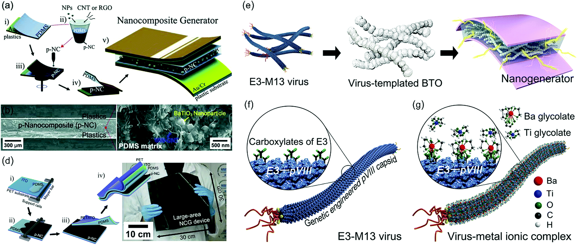 | ||
| Fig. 1 (a) Schematic illustration of the process for fabricating a flexible nanocomposite generator. (b) A cross-sectional SEM image of an NCG device. (c) A magnified cross-sectional SEM photograph of the p-NC.68 Reprinted with permission from ref. 68. Copyright©2012 Wiley-VCH Verlag GmbH & Co. KGaA, Weinheim. (d) Schematic diagram showing the fabrication process of a large-area flexible nanocomposite generator device (30 cm × 30 cm) using the Mayer bar-coating method.71 Reprinted with permission from ref. 71. Copyright©2013 Wiley-VCH Verlag GmbH & Co. KGaA, Weinheim. (e) Overall fabrication process of a virus-templated BTO based piezoelectric nanogenerator. (f) An M13 bacteriophage is shown with the major genetically engineered capsid proteins (pVIII). Three glutamates (E3) are expressed on the N-terminus of pVIII. (g) Virus-metal ion complexation occurs when barium/titanium glycolates interact with E3 modified coat proteins.70 Adapted with permission from ref. 70. Copyright©2013 American Chemical Society. | ||
2.2 Etching of a sacrificial layer
The output performance of nanocomposite generators is limited by their poor piezoelectric properties76,77 and low energy conversion rates owing to the utilization of two sandwiched plastic substrates or thick piezoelectric polymer layers.68,71,74 To enhance the conversion efficiency of energy harvesting devices, researchers have attempted to transfer a ferroelectric thin film onto flexible substrates from parent substrates to utilize the high inherent piezoelectric properties of the FE thin film. The main challenge is the successful and intact separation of the thin films from the substrates. The FE film can be transferred onto a flexible substrate through standard microfabrication and soft lithographic printing techniques.64,66,78–80 In this process, a sacrificial layer is inserted between the FE film and the substrate, where SiO2,66,79 (La,Sr)MnO381 and MgO82 have been reported as sacrificial layers. A FE thin film can be synthesized easily and cheaply via a sol–gel process66,79 and RF magnetron sputtering78 on an oxidized silicon wafer coated with Pt/Ti, and etching with SiO2 has been widely used in the semiconductor industry. Fig. 2 presents a detailed experimental process. First, an FE thin film and top electrode were deposited on a Pt/Ti/SiO2/Si substrate. Second, the array capacitor structures (metal–insulator–metal, MIM) were etched via dry or wet chemical etching methods. The underlying SiO2 was removed using diluted HF (H2O![[thin space (1/6-em)]](https://www.rsc.org/images/entities/char_2009.gif) :HF (49%) = 1:3) to separate the MIM structure ribbons from the parent substrates. Third, a polydimethylsiloxane (PDMS) stamp was placed in uniform contact with the top surface of the freestanding MIM structure ribbons. Upon quick removal from the Si wafer, the array MIM structure ribbons were transferred onto the PDMS. Fourth, transfer of the MIM structure ribbons onto a plastic substrate. An elastomer slab, inked with MIM structure ribbons, was then placed on a polyurethane (PU)-coated plastic substrate (Kapton film, 100 μm in thickness). The PU was optically cured using ultraviolet light. The MIM structure ribbons were well settled on a plastic substrate when the PDMS was peeled away.
:HF (49%) = 1:3) to separate the MIM structure ribbons from the parent substrates. Third, a polydimethylsiloxane (PDMS) stamp was placed in uniform contact with the top surface of the freestanding MIM structure ribbons. Upon quick removal from the Si wafer, the array MIM structure ribbons were transferred onto the PDMS. Fourth, transfer of the MIM structure ribbons onto a plastic substrate. An elastomer slab, inked with MIM structure ribbons, was then placed on a polyurethane (PU)-coated plastic substrate (Kapton film, 100 μm in thickness). The PU was optically cured using ultraviolet light. The MIM structure ribbons were well settled on a plastic substrate when the PDMS was peeled away.
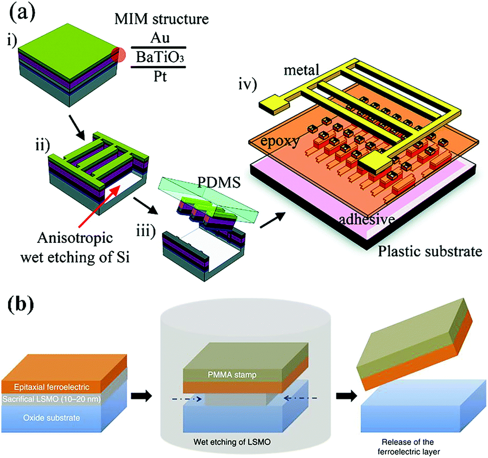 | ||
| Fig. 2 (a) Schematic illustration of the process for fabricating a flexible BaTiO3 nanogenerator on plastic substrates.78 Adapted with permission from ref. 78. Copyright©2010 American Chemical Society. (b) Transfer process. Epitaxial thin films of ferroelectric oxides are grown on lattice-matched substrates with a thin (10–20 nm) sacrificial layer via pulsed laser deposition method. The stack is then immersed in a diluted KI + HCl solution, which isotropically etches La0.7Sr0.3MnO3. A polymethyl methacrylate handle is used to transfer the released ferroelectric layers onto Si and other substrates.81 Reprinted with the permission from ref. 81. Copyright©2016, Springer Nature. | ||
(La,Sr)MnO3 was used as another sacrificial layer81 in the thin film structure of an epitaxial FE Pb(Zr,Ti)O3 film grown on SrTiO3 single-crystal substrates and (La,Sr)MnO3 was etched using diluted KI + HCl solution (the transfer process is presented in Fig. 2(b)). The low production, which is limited by the small contact area (five or ten square millimeters) between the plume and substrates and the long time (at least six hours) to achieve high vacuum and high temperature conditions, are the biggest hurdles for industrial application of pulse laser deposition technology. The sol–gel method on the other hand has the advantages of being suitable for mass production, short reaction time and low cost, but the films produced are polycrystalline or textured. In addition, the FE thin films can also be damaged by the etching solution.
2.3 Laser lift-off process
The laser lift-off process has been developed for twenty years and was initially used to fabricate high-quality epitaxial GaN films for light-emitting diodes.63,83 An excimer laser was used to bombard the GaN film. Due to the strong absorption and interaction between the laser and GaN, with a very short pulse of the excimer laser, the epitaxial GaN film can be detached from the sapphire substrate. The laser lift-off (LLO) process39,40 can also be used to transfer a FE thin film onto flexible substrates from parent substrates to provide a simple, stable, and large-area transfer method for the preparation of highly piezoelectric thin films onto flexible substrates annealed at high temperature. Compared to the etching process of a sacrificial layer, the LLO process can prevent corrosion of the FE thin film by the etching solution and transfer a full film onto flexible substrates from parent substrates. First, an FE thin film was deposited on a double-side polished sapphire substrate using a conventional sol–gel method. Second, the crystallized FE thin film on the sapphire wafer was fixed to a flexible polyethylene terephthalate (PET) substrate via ultraviolet light-enabled curing of polyurethane adhesive. Third, the FE thin film was removed from the bulk sapphire wafer by irradiating the underside of a sapphire substrate with a XeCl-pulsed excimer laser (wavelength of 308 nm). The detailed experimental process is shown in Fig. 3(a). The XeCl laser has a photon energy of 4.03 eV (corresponding to an energy density of 420 mJ cm−2), which is located between the band gap energies (Eg) of sapphires (Eg = 10 eV) and PZT ceramics (Eg = 3.2–3.6 eV),37,40,62 irradiated laser beams can pass through the transparent sapphires and then locally vaporize the interface between the FE layer and the sapphire substrate, thus separating the FE thin film from the sapphire parent substrate. Flexible lead zirconate titanate thin film (PbZr0.52Ti0.48O3, PZT) is the most reported FE/piezoelectric material owing to its large piezoelectric and electromechanical coupling coefficients, high dielectric permittivity and significant remnant polarization.84 PZT-based materials are usually used in ultrasonic transducers,85 microelectromechanical devices and actuators,86 as well as pressure87 and strain88 sensors.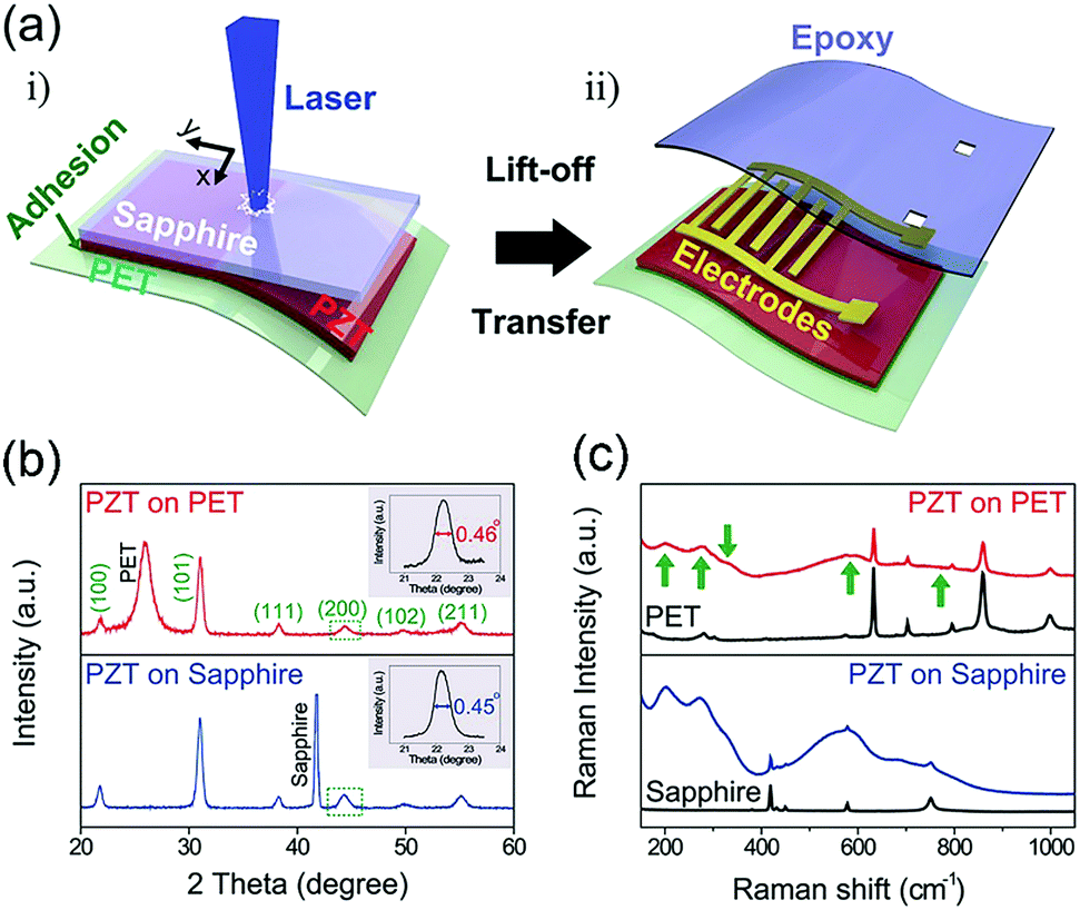 | ||
| Fig. 3 (a) Schematic diagram of the fabrication process for a PZT thin film-based NG using the LLO method. (b) XRD analysis results of PZT thin films on flexible (top, red) PET and sapphire (bottom, blue) substrates. The insets show the XRD rocking curves of the (200) peaks. (c) Raman spectra observed for the PZT thin films before and after the LLO process.62 Reprinted with permission from ref. 62. Copyright©2014 Wiley-VCH Verlag GmbH & Co. KGaA, Weinheim. | ||
2.4 Direct growth
FE thin films can also be directly grown on flexible substrates through van der Waals heteroepitaxy. Koma89–91 first fabricated many kinds of heterostructures using van der Waals epitaxy. Superconductor, metal, semiconductor or insulator films are some of the selected materials. This method uses a variety of transition metal dichalcogenides and other materials without dangling bonds on their surfaces as substrates. Thus, only weak van der Waals forces exist across the interface between the film and substrate. By taking advantage of key features such as epitaxy, which involves weak van der Waals interactions between layers, a high-quality film with reduction of defects, tolerance of lattice match and which is almost strain-free can be obtained. Muscovite (mica, KAl2(Si3Al)O10(OH)2: a = 5.33 Å, b = 9.23 Å, c = 10.22 Å, and β ∼ 100°) possesses many key advantages, including an atomically flat surface, high thermal stability (especially for fluorphlogopite substrates, up to 1000 °C), chemical inertness, high transparency in ultrathin thickness, mechanical flexibility and compatibility with present fabrication methods, and is thus considered as the most suitable substrate for van der Waals epitaxy.92–94 Moreover, muscovite exhibits very high yield strain and a single cleaved mica sheet with superior flexibility can be obtained via mechanical exfoliation. It is reported that the thickness of muscovite sheets can be down to 100 nm and they can show a minimum band radius less of than 0.03 cm.95 An epitaxial PZT thin film deposited directly on flexible mica substrate via van der Waals epitaxy was reported,67,95,96 the growth scheme of which is shown in Fig. 4(c). A flexible mica/SRO/PZT/Pt capacitor shows saturated P–E loops under different bending conditions and a large saturated polarization (PS) of ≈60 μC cm−2 under flat conditions (Fig. 4(e)). Fig. 4(f) indicates that ferroelectric polarization shows no obvious decay even after the mica/SRO/PZT/Pt capacitors are bent to a 2.2 mm radius 10000 times. Yang et al.95 reported that ferroelectric polarization shows almost no loss within 107 switching cycles, while the initial polarization value is reduced by ≈21% in fatigue cycling up to 109. These single-crystalline flexible fluorphlogopite PZT thin films exhibit excellent properties in unbent and bent states, and can retain their reliability and thermal stability, comparable to those grown on substrate counterparts. In addition, the PZT/mica heterostructure shows good fluorphlogopite properties at a bending radius down to 2.5 mm, which also suggests that the PZT/mica heterostructure exhibits remarkable mechanical properties. Some other functional oxide thin films such as ITO and AZO,50 VO2,51 MoO2,96 SrRuO3,52 CoFe2O4,97 and Cu Fe2O498 can also be fabricated via van der Waals epitaxy on mica substrate. The crystal structure and physical and chemical characteristics of mica, and the detailed growth mechanism and applications of the functional oxides on mica have been summarized in recent reviews.90,92,99
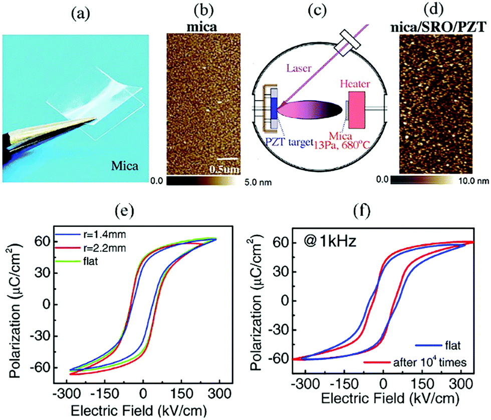 | ||
| Fig. 4 Growth scheme. (a) Mechanical peeling of a 10 μm substrate from a layer-stacked mica crystal. (b) AFM image of the surface of the mica. (c) PZT films were grown on mica at 680 °C and 10 Pa oxygen pressure. (d) AFM image of the surface of the PZT film. (e) P–E loops of the PZT film measured at 1000 Hz in flat, 2.2 mm radius, and 1.4 mm radius SRO/PZT/Pt capacitors. (f) P–E loops before and after the PZT film was bent to a 2.2 mm radius 10000 times.94 Reprinted with permission from ref. 94. Copyright©2017 Wiley-VCH Verlag GmbH & Co. KGaA, Weinheim. | ||
3. Biomedical sensors
FE materials can convert tiny vibrations to an electrical signal due to their high piezoelectric coefficient. Hence, these materials can be used to fabricate bio-implantable or wearable biomedical sensors for monitoring cellular deformations,100 gastrointestinal motility,101 blood pressure,41,79 soft tissue biomechanics66 and energy harvesting and storage from motions of the heart, lungs, and diaphragm.64,80 In addition, biomimetic artificial hair cells,40 self-powered cardiac pacemakers102 and self-powered deep brain stimulation devices103 can also be fabricated based on inorganic FE materials.3.1 Implantable biomedical sensors
Bioelectrical signals can be generated by different sensory organs of the human body and play an important role during the transmission of information by the nervous system. Meanwhile, bioelectrical signals are an essential index of physiological parameters of the human body and have broad relevance in clinical diagnosis and the treatment of disease. ZnO nanowires were first fabricated as a nanogenerator due to their piezoelectricity, which can generate electricity in response to ambient mechanical stimuli including gentle airflow, ocean waves, motor vibration, and even slight movements of human organs/muscles.42,104 A PZT ferroelectric thin film exhibits an exceptional piezoelectric charge constant of ∼60 to 130 pC N−1, which is almost 10–20 times higher than that of ZnO (5.9 pC N−1).61 Recently, some implantable electronics fabricated using PZT thin films have been widely used to assist some damaged organs of a patient's body and monitor some health conditions, including artificial cochlea,40 cardiac pacemakers102 and deep brain stimulation devices,103 amongst others. These prototype implantable biomedical devices will be reviewed in this section.Hair cells are located all along the basilar membrane (BM) and convert sound-induced vibrations of the BM into electricity to stimulate auditory nerves. If these hair cells are lost or damaged due to various factors, the damaged hair cells can no longer generate an electrical potential, resulting in permanent hearing impairment such as sensorineural hearing loss (SNHL).105 Fortunately, piezoelectric materials have the same function as hair cells in that they can transfer mechanical vibrations to electric signals, suggesting that they could be used in place of hair cells to create an artificial cochlear epithelium.40,105 Inaoka et al.105 first reported an artificial cochlea epithelium using an organic piezoelectric membrane to mimic the functions of mammalian hair cells. However, the electrical output power was not sufficient to stimulate the auditory nerves directly due to the relatively low piezoelectric charge constant.6,9,10 In order to generate sufficient output power, an inorganic piezoelectric material such as PZT is the better choice. Lee et al.40 reported a highly efficient and flexible inorganic piezoelectric acoustic nanosensor using a PZT thin film as a biomimetic artificial hair cell, as presented in Fig. 5(a), with which vibration displacements of 7 to 17 nm and piezoelectric signals of 45 to 60 μV can be measured. A finite element analysis simulation method was used to identify the electrical response of a flexible PZT film to the motion of the BM. The simulated piezopotential from the PZT film is approximately 3 V, which is sufficient to simulate the auditory nerves without an additional power supply.
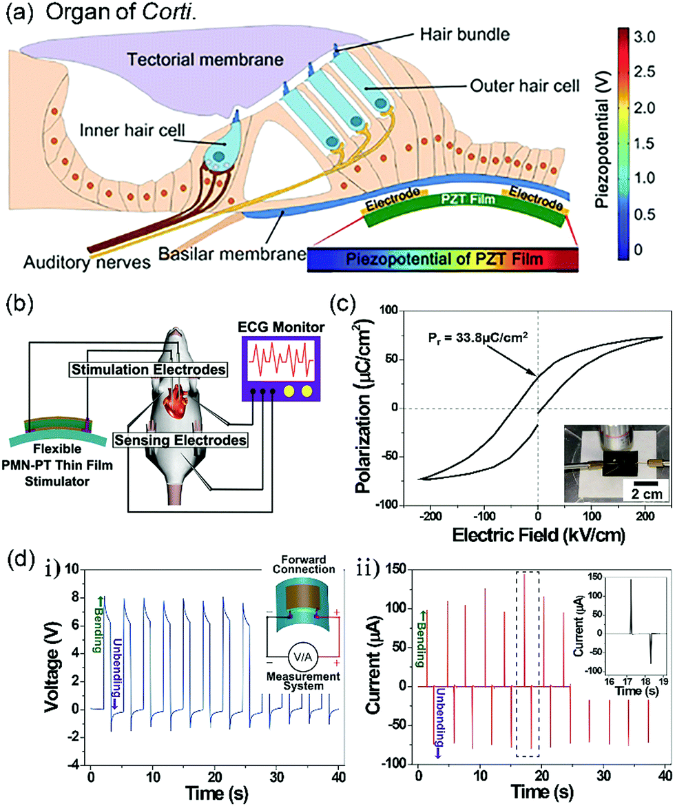 | ||
| Fig. 5 (a) Conceptual schematic of the organ of Corti in mammalian cochlea.40 Reprinted with permission from ref. 40. Copyright©2014 Wiley-VCH Verlag GmbH & Co. KGaA, Weinheim. (b) Schematic illustration of artificial cardiac pacemaking using electrical energy from a flexible PMN–PT energy harvester. (c) Polarization–electric field hysteresis loop of a ferroelectric PMN–PT thin film on PET. (d) The open-circuit voltage (i) and short-circuit current (ii) signals generated from the energy harvester in forward connection during periodical bending and unbending motions.102 Reprinted with the permission from ref. 102. Copyright©2014 Wiley-VCH Verlag GmbH & Co. KGaA, Weinheim. | ||
Sick sinus syndrome or heart blockage can cause abnormal heart rate, and may result in syncope, angina, dizziness, and even heart failure, which seriously threaten human health. Artificial cardiac pacemakers, which use electrical impulses to contract the heart muscles,106 have made a significant contribution to regulate heartbeat. However, the lifespan of the battery (7 to 10 years) makes it necessary to undergo replacement surgery of an artificial pacemaker implanted beneath chest skin.107,108 The frequent invasive medical procedures for replacing batteries involve the risk of inflammation as well as being a financial burden to patients.109 A self-powered cardiac pacemaker is an attractive approach to address this challenge, which can potentially provide features such as low maintenance, independent operation, and sustainability for implantable biomedical devices.110 Lee et al.102 designed a self-powered artificial pacemaker (Fig. 5(b)) based on a flexible and highly-efficient energy harvester enabled by a single-crystalline piezoelectric PMN–PT thin film grown on a plastic substrate, exhibiting good ferroelectric properties with a high remnant polarization of 33.8 μC cm−2 at a maximum applied field of 225 kV cm−1 (Fig. 5(c)). The maximum output current and voltage of the flexible PMN–PT thin film harvester reach 145 μA and 8.2 V (as shown in Fig. 5(d)), respectively, which is sufficient to drive a cardiac pacemaker (operating at an input of 100 μA and 3 V).123,124 In addition, the output current was consistent without noticeable degradation during 30000 continual bending cycles of the device at a curvature radius of 16.5 mm. A flexible FE energy harvester can also be applied for deep brain stimulation (DBS), which is a neurosurgical procedure for the stimulation of a specific brain area with electrical pulses and is widely used for neural prosthetics and brain–computer interfacing.111,112 Lee et al.103 developed a self-powered deep brain stimulation device via a flexible energy harvester and the output current signals were steady without any notable changes during ∼15000 bending and unbending cycles at a bending radius of 20.5 mm, generating an extremely high current reaching 0.57 mA with slight bending to satisfy a high threshold current for real-time DBS of the motor cortex. In addition, Traverso et al.101 reported flexible piezoelectric devices for gastrointestinal motility sensing to monitor vital signs and associated mechanical deformations of the gastric cavity. Therefore, it can in turn aid in the diagnosis and treatment of motility disorders, and monitoring of ingestion for the treatment and evaluation of obesity.
3.2 Wearable biomedical sensors
Compared to implantable biomedical devices, wearable biomedical sensors work in vitro and have the advantage of being noninvasive. This section will introduce some wearable biomedical sensors used in blood pressure monitoring,41,79 measurement of soft tissue viscoelasticity66 and detection of the mechanical response of mammalian cells.100Blood pressure (BP) is one of the most important physiological parameters of human beings, which reflects the functional state of the heart and peripheral vascular resistance.113,114 Accurate and timely measurement of blood pressure is useful to diagnose disease, observe the changes of disease condition and judge treatment effect.115 Most national anesthesiology societies recommend BP monitoring at least once every 5 min in anesthetized subjects undergoing surgical procedures.115 Continuous monitoring of blood pressure during hypertensive treatment, in evaluation of the hemodynamic effects of atherosclerotic risk factors or in projections of life-threatening cardiovascular events.79
However, the use of sphygmomanometers to continuously monitor blood pressure in the long term is difficult, which is limited by the stationary setup and expensiveness of sphygmomanometers. The development of thin film preparation technology has led to the facile fabrication of flexible sensitive strain sensors. Dagdeviren et al.79 reported a novel pressure sensor with a capacitor-type structure for continuously monitoring blood pressure, as shown in Fig. 6(a). The sensor, which consists of an array of square elements of high-quality PZT thin sheets to induce a voltage across the device, and is collectively connected to the gate electrodes of an adjacent SiNM n-MOSFET which can amplify the piezoelectric voltage response and convert it to a current output via capacitance coupling. This novel flexible pressure device can accommodate 30% uniaxial strain without any degradation in operating characteristics. Experimental studies reveal that the sensor shows low hysteresis measurements of pressure on the skin, high levels of sensitivity (∼0.005 Pa) and fast response times (∼0.1 ms). Lee et al.41 integrated a self-powered flexible piezoelectric pulse sensor with a signal processing circuit composed of amplifiers, comparators, and output modules to identify tiny arterial pulses. And then, the pulse signal was wirelessly transmitted to a smart phone for real-time monitoring using a microcontroller and a Bluetooth transmitter.
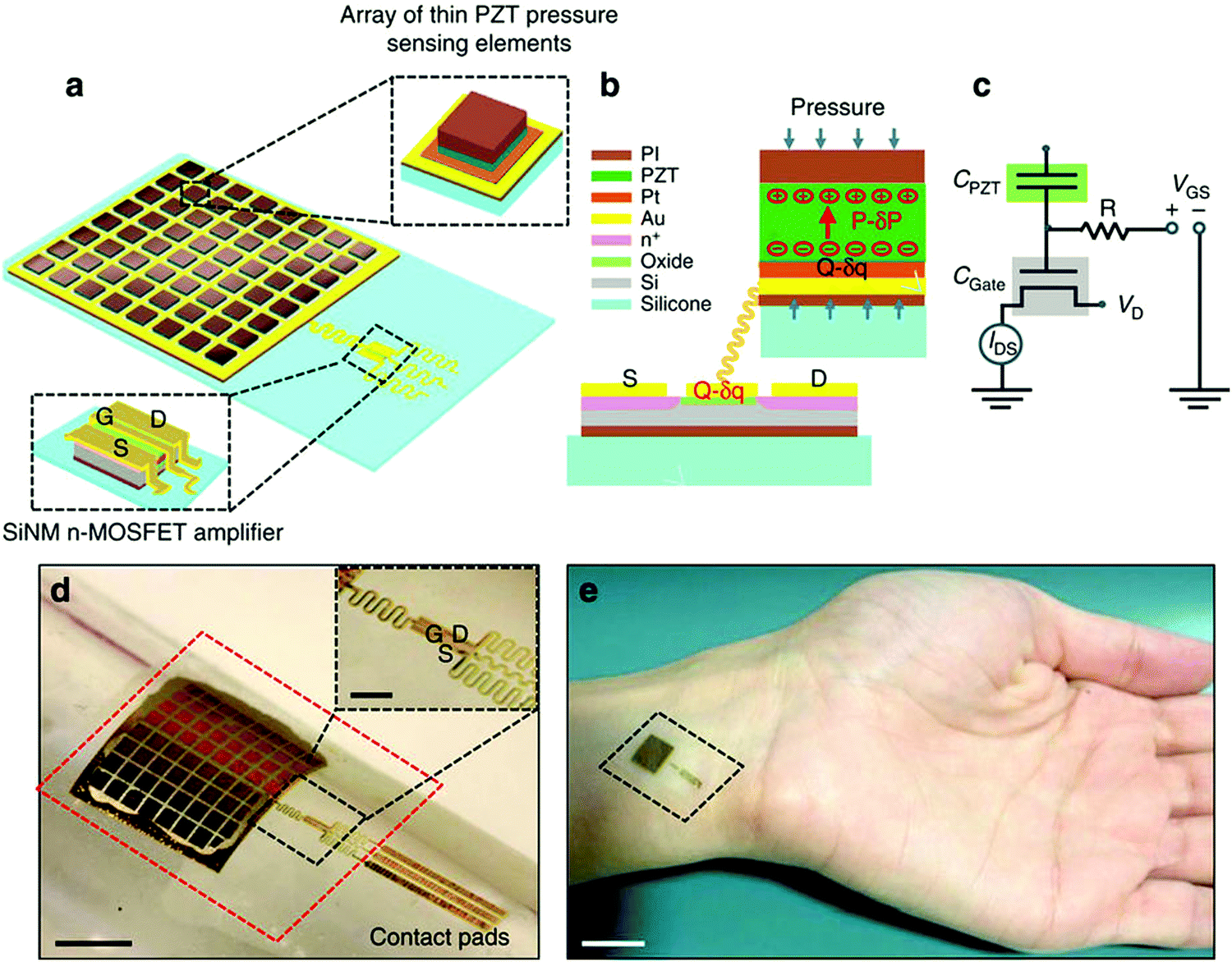 | ||
| Fig. 6 (a) Schematic illustrations and photographs of a thin conformable piezoelectric pressure sensor. (b) Cross-sectional schematic illustration of a pressure sensor and its connections to an associated transistor. (c) Equivalent circuit for capacitance coupling between the pressure sensor and the transistor. (d) Photograph of a device wrapped on a cylindrical glass support. (e) Photograph of a device stuck on a wrist.79 Reprinted with the permission from ref. 79. Copyright©2014, Springer Nature. | ||
Changes in the elastic modulus of the skin are signs of disorders such as scleroderma, Ehlers-Danlos syndrome, psoriasis, eczema, melanoma, and other cutaneous pathologies. Thus, understanding the mechanical properties of the skin are centrally important in diagnosis and treatment.116,117 Dagdeviren et al. developed conformal and piezoelectric devices that enable in vivo measurements of soft tissue viscoelasticity in the near-surface regions of the epidermis under both quasi-static and dynamic conditions.66 These devices can measure the skin elastic modulus precisely, rapidly and non-invasively under various conditions, and can facilitate the assessment of a variety of pathophysiological conditions, may predict reactions to exogenous substances and environmental factors,117 can help in gauging the effectiveness of cosmetic products and further establish mechanisms associated with growth, repair and ageing.
Methods of detecting the electrical and mechanical response of mammalian cells to electrical excitations can improve our understanding of cellular physiology and function. The electrical response of neuronal cells to applied voltages has been studied in detail, but their mechanical response to electrical excitations has not been investigated due to their small size, irregular shape and fragility. A PZT nanoribbon-based sensor has been designed by Nguyen et al.100 to probe the tiny deformations of cells, where 1 nm depressing of cells can be measured when 120 mV is applied to the cell membrane. However, despite its remarkable properties, this sensor still exhibits problems when implanted due to the toxicity of lead.
4 Energy harvesters
Since Wang and co-workers42 first reported the use of zinc oxide (ZnO) nanowire arrays to fabricate a nanogenerator, various piezoelectric materials such as BaTiO3, PVDF, PZT, PMN–PT and so on have been used. Recently, perovskite piezoelectric materials have drawn more attention than ZnO and PVDF in the field of energy harvesters due to their high piezoelectric coefficients.61 In addition, triboelectric energy conversion devices based on a triboelectric effect have also experienced tremendous growth, but have been discussed in recent reviews,118 and will therefore not be discussed in this review. Here, we focus on the different structures of energy harvesters and their working principle. Nanowire arrays, nanoribbons, metal insulator (FEs) metals (MIMs) and interdigitated electrodes (IDE)-based prototype devices have been designed to harvest mechanical energy.4.1 Nanofibers and nanoribbon-based devices
Chen et al.119 reported a nanogenerator based on laterally aligned PZT nanofibers on interdigitated electrodes of fine platinum wires packaged using a soft polymer on a silicon substrate, as shown in Fig. 7(a). The piezoelectric nanofibers between each pair of adjacent electrodes serve as unit cells, and each cell is connected in parallel to generate a peak output voltage of 1.63 V and output power of 0.03 μW (Fig. 7(e)). The PZT nanofibers were fabricated by electrospinning with a diameter and length of approximately 60 nm and 500 μm. The power generation mechanism is illustrated in Fig. 7(b) and (c), where alternating pressure applied on the PZT nanofibers results in charge generation, and then a voltage difference between the two adjacent electrodes is thereby induced due to the separation of charge. Electrons generated in the PZT nanofibers can transfer through the electrodes when the PZT nanofibers are subjected to external stresses.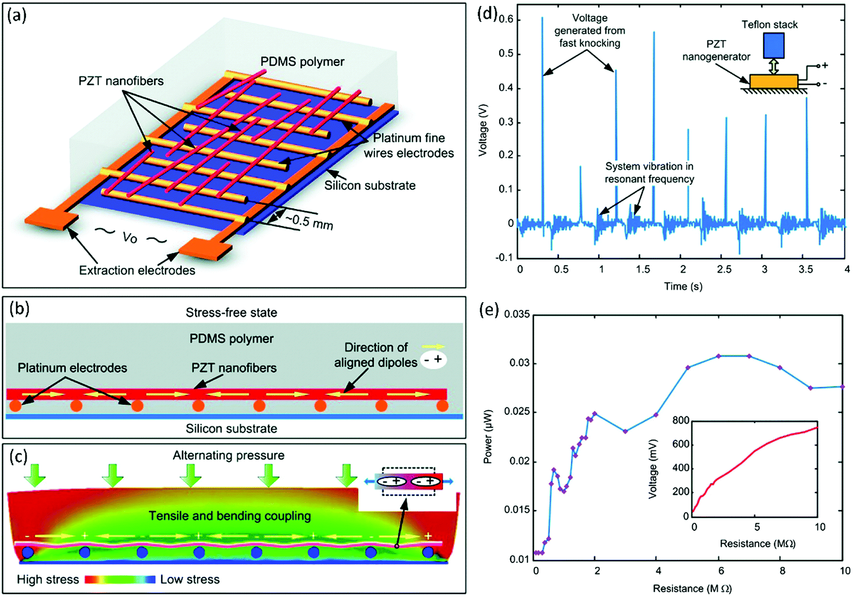 | ||
| Fig. 7 (a) Schematic view of a PZT nanofiber generator. (b) Cross-sectional view of the polled PZT nanofiber in the generator. (c) Schematic view showing the power output mechanism of the PZT nanofibers. (d) Voltage output measured when a small Teflon stack is used to impart an impulse load on the top of the PZT nanofiber generator. (e) The power delivered to the load resistors versus the load resistance.119 Adapted with permission from ref. 119. Copyright©2010 American Chemical Society. | ||
The d33 values of 54.2 and 101.0 pm V−1 for the PZT ribbons before and after poling were reported, which agree well with the thin film data.120 In addition, PZT ribbons with a wavy/buckle structure induced by prestrained PDMS were fabricated and showed an enhancement in the piezoelectric effect of up to 70%.121 Thereby, PZT nanoribbons are a promising hybrid material platform for wearable and implantable energy harvesting devices.
Junggou Kwon et al.122 integrated the PZT nanoribbons with graphene film as electrodes, as shown in Fig. 8(a) and (b). The power generation mechanism of the PZT nanoribbon-based nanogenerator is similar to that of a PZT nanofiber-based nanogenerator. The PZT nanoribbon-based nanogenerator shows a high output voltage of ∼2 V, current density of ∼2.2 μA cm−2 (Fig. 8(c) and (d)) and power density of ∼88 mW cm−3 when an external force of 0.9 kgf is applied, which is higher than for PZT nanofibers (1.63 V and 0.03 μW). This may be due to the nanofibers being randomly aligned, causing degradation in net polarization and developing relatively less piezopotential under external mechanical stress, whereas the nanoribbons were created using a conventional photolithographic method and well arrayed on graphene interdigitated electrodes. Qi and co-workers121 presented wavy PZT ribbons on silicone rubber with a high energy density of 2.5 μA mm−2. These studies demonstrate that nanoribbons are superior to nanofibers in the field of energy harvesters.
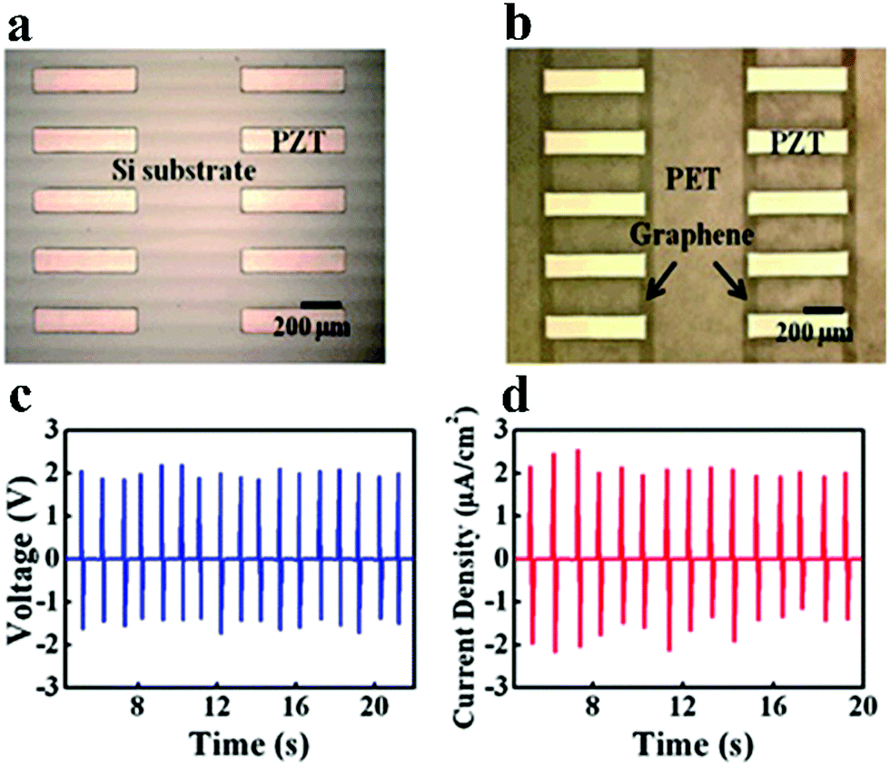 | ||
| Fig. 8 (a) Optical image of PZT nanoribbons on a silicon wafer. (b) PZT nanoribbons with graphene electrodes on PET film. (c) The voltage and (d) current density of a PZT nanogenerator with doped graphene electrodes when a dynamic load was applied on top of the generator by touch.122 Reproduced from ref. 122 with permission from The Royal Society of Chemistry. | ||
4.2 Metal insulator (FEs) metal (MIM)-based devices
The fabrication process of MIM-based nanocomposite generators is discussed in Section 2.1. The mechanism of the generation of electrical energy from the device is depicted in Fig. 9(a). Upon exposing a FE element to a strong electric field, most dipole moments will be aligned with the direction of the field, as shown in the original state of the nanocomposite generator (NCG) device (Fig. 9(a)-i). When the NCG device is subjected to mechanical deformation via a bending motion (Fig. 9(a)-ii), a piezoelectric potential is produced between the top and bottom electrodes because of dipoles in the p-NC. Due to the insulating p-NC layer, electrons can flow through the external circuit to balance the field made up of dipoles and accumulate at the interface of the top electrodes. This behavior generates electrical signals of voltage and current. As the NCG device is released (Fig. 9(a)-iii), the strain and the piezopotential disappear.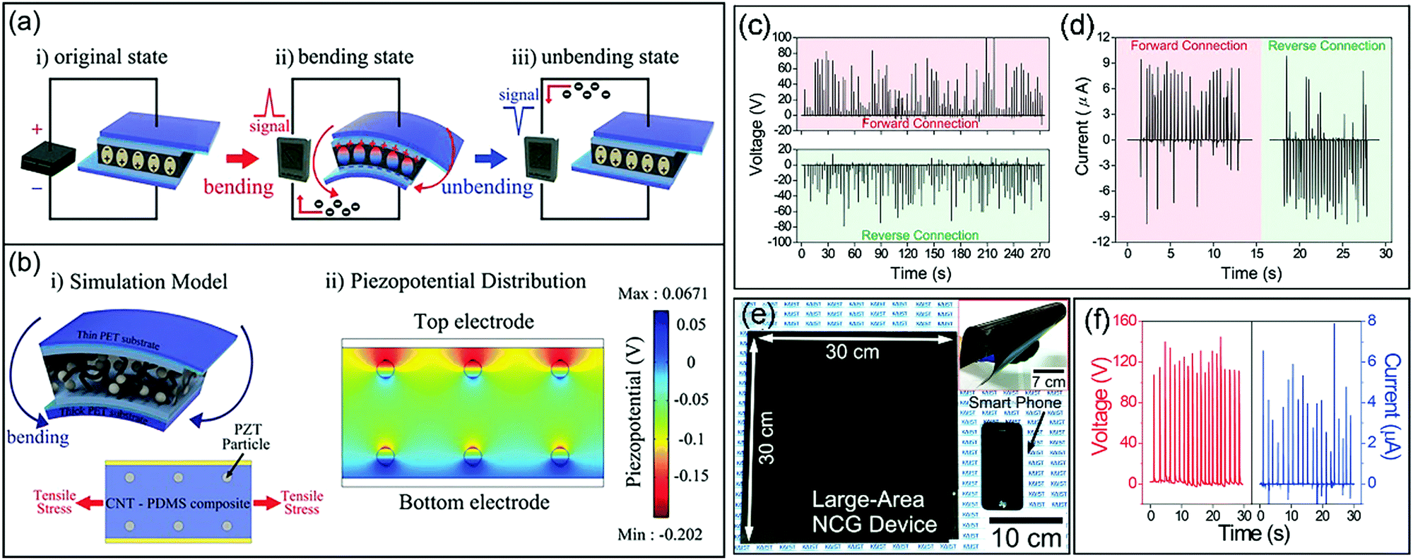 | ||
| Fig. 9 (a) Working mechanism of a MIM-based nanogenerator. (b) Simulation model (left, i) and piezoelectric potential distribution (right, ii) inside a NCG device. The measured (c) output voltage and (d) current signals from the NCG device during irregular deformation by human hand tapping.71 Reprinted with permission from ref. 71. Copyright©2013 Wiley-VCH Verlag GmbH & Co. KGaA, Weinheim. (e) Digital photograph of a KNLN-based large-area NCG device (30 cm × 30 cm) fabricated using a bar-coating method. (f) The generated output voltage and current signals from the NCG device, with forward connection of the measurement unit, during irregular mechanical impact by hand clapping.73 Reprinted with permission from ref. 73. Copyright©2014 Wiley-VCH Verlag GmbH & Co. KGaA, Weinheim. | ||
Lee et al.68 reported a nanocomposite nanogenerator based on BTO nanoparticles (synthesized via a hydrothermal reaction) and multi-walled carbon nanotubes. The nanogenerator generates an open-circuit voltage (Voc) of ∼3.2 V and a short-circuit current (Isc) signal of 250 to 350 nA. They also synthesized BTO nanocrystals on an M13 viral template through the genetically programmed self-assembly of metal ion precursors and this nanogenerator shows a higher electrical output of up to ∼300 nA and ∼6 V, attributed to the enhanced performance to the inherently dispersed structure of virus-templated nanocrystals.70 BTO particles can also be mixed with organic FE materials (PVDF) to improve their piezoelectric power output. Shin et al.123 reported a BTO–P(VDF–HFP) composite-based nanogenerator that exhibits a high electrical output of up to ∼75 V and ∼15 μA with applied force normal to the surface. A large-area nanogenerator device (30 cm × 30 cm, as shown in Fig. 9(e)) can also be fabricated using piezoelectric alkaline niobate-based particles (KNLN) and a copper (Cu) nanorod filler via a bar-coating method to obtain a maximum output of up to 140 V and 8 μA (Fig. 9(f)).73
The electrical output of the NCG can be significantly increased using PZT particles as an energy generation source due to their excellent piezoelectric properties. A high output voltage and current signals of ∼100 V and 10 μA (Fig. 9(c) and (d)) can be generated in a PZT-based NCG (30 cm × 30 cm).71 The FE nanowires or nanofiber-based nanogenerator show a higher output voltage than that based on particles. Cung et al.72 presented a NCG based on PZT nanowires, which has an output power density of 0.82 μW cm−2. A PMN–PT nanowire-based nanogenerator demonstrates a high output voltage of up to 7.8 V and an output current of up to 2.29 μA (current density of 4.58 μA cm−2).74
4.3 Interdigitated electrode (IDE)-based devices
However, despite the remarkable potential for use of NCGs as flexible energy harvesters, they still show low energy conversion rates owing to the utilization of two sandwiched plastic substrates or thick piezoelectric polymer layers.68,71–75 In addition, these nanocomposites degrade rapidly in air.121 In order to improve the conversion efficiency of NGs, researchers have transferred high-quality piezoelectric thin films from a host substrate to plastic substrate.37–39,62 The open-circuit voltage (V3j) generated when piezo-materials are deformed by mechanical stress (σxx) can be expressed as in eqn (1),| V3j = σxxg3jLj | (1) |
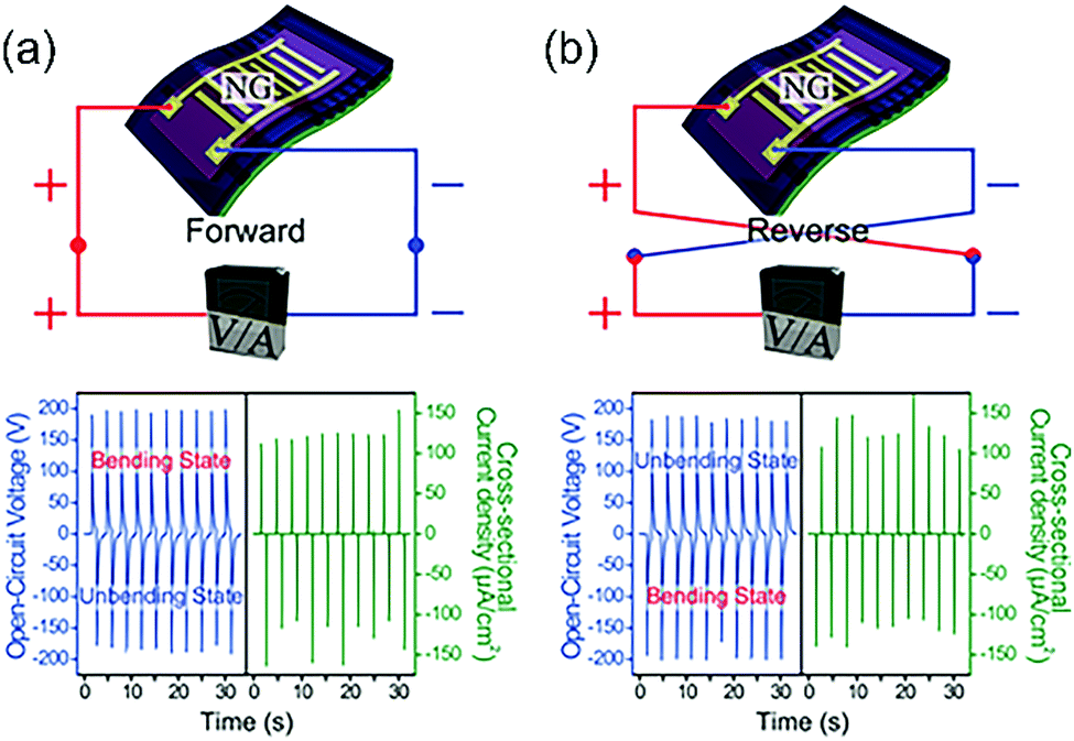 | ||
| Fig. 10 (a and b) The open-circuit voltage and cross-sectional current density measured from a PZT thin film NG in (a) forward and (b) reverse connections.62 Reprinted with permission from ref. 62. Copyright©2014 Wiley-VCH Verlag GmbH & Co. KGaA, Weinheim. | ||
The working mechanism of an IDE-based NG can be explained via the piezoelectric effect between each pair of adjacent electrodes (Fig. 11(a)-ii–iv). The polarization direction becomes parallel to the surface of the PZT thin film upon applying a high electric field at high temperature, in a process known as poling (Fig. 11(a)-ii). When the NG device is bent along the direction perpendicular to the IDEs, as shown in Fig. 11(a)-iii, positive and negative piezopotentials are generated at neighboring electrodes, which is the driving force for the electrons to flow in an external load. Subsequently, when the bending stress of the NG is released (Fig. 11(a)-iv), the piezopotential at each pair of adjacent electrodes vanishes and the electrons then move back to their original positions, generating reverse output signals.62 Rectifier circuit, which can convert discontinuous alternating current (AC) peaks into constant direct current (DC) output for external electronics, is another critical issue related to flexible piezoelectric energy harvesting.124 Lee et al.125 designed a reconfigurable rectifying circuit system integrated with a flexible PMN–PZT energy harvester (the schematic circuit diagram is given in Fig. 12). This system can provide a steady output voltage of 5–6 V to external 2 kΩ load resistors.
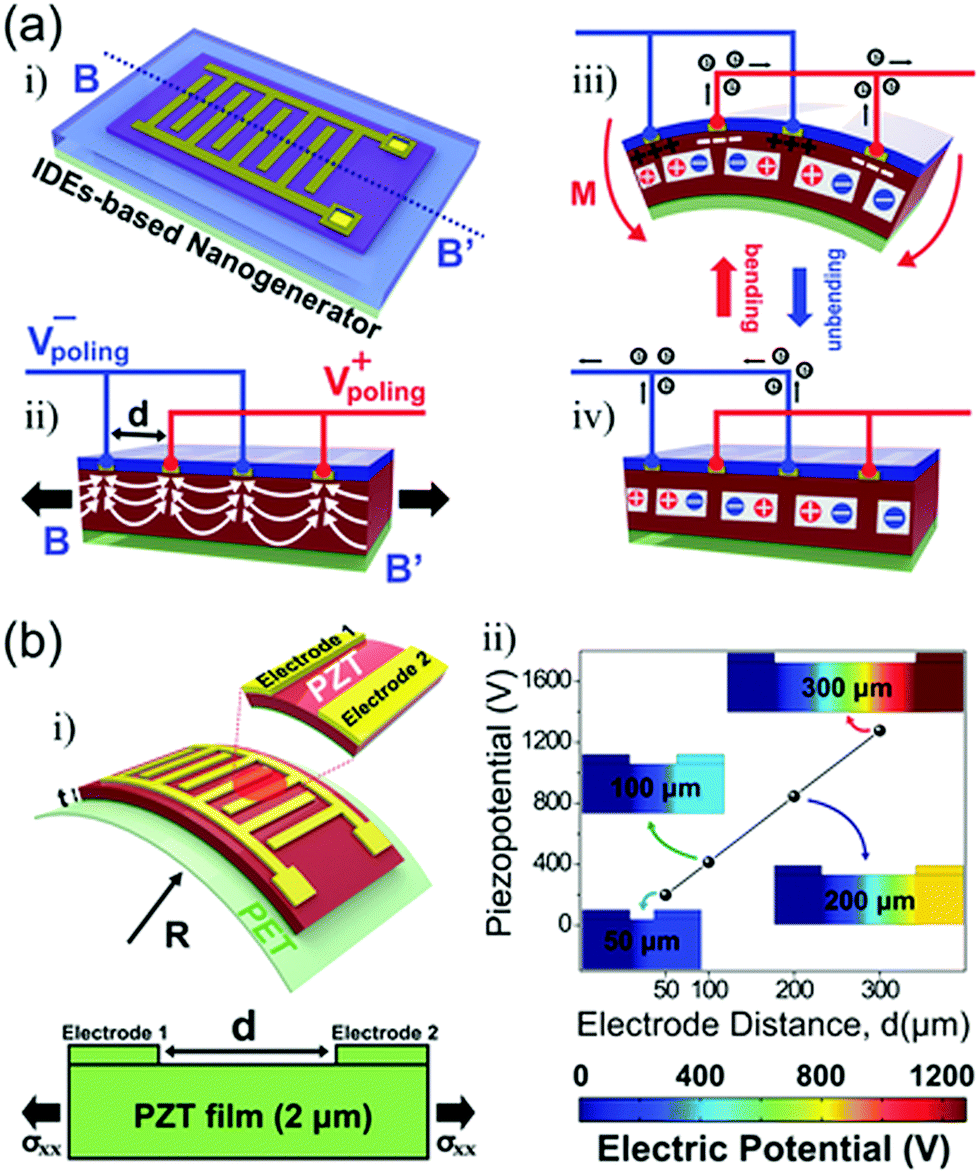 | ||
| Fig. 11 (a) Schematics of the working principle of a flexible PZT thin film NG. (b) Simulation model of an IDE-based thin film NG (i) and the piezopotential generated inside PZT thin film with different distances between adjacent electrodes (ii).62 Reprinted with permission from ref. 62. Copyright©2014 Wiley-VCH Verlag GmbH & Co. KGaA, Weinheim. | ||
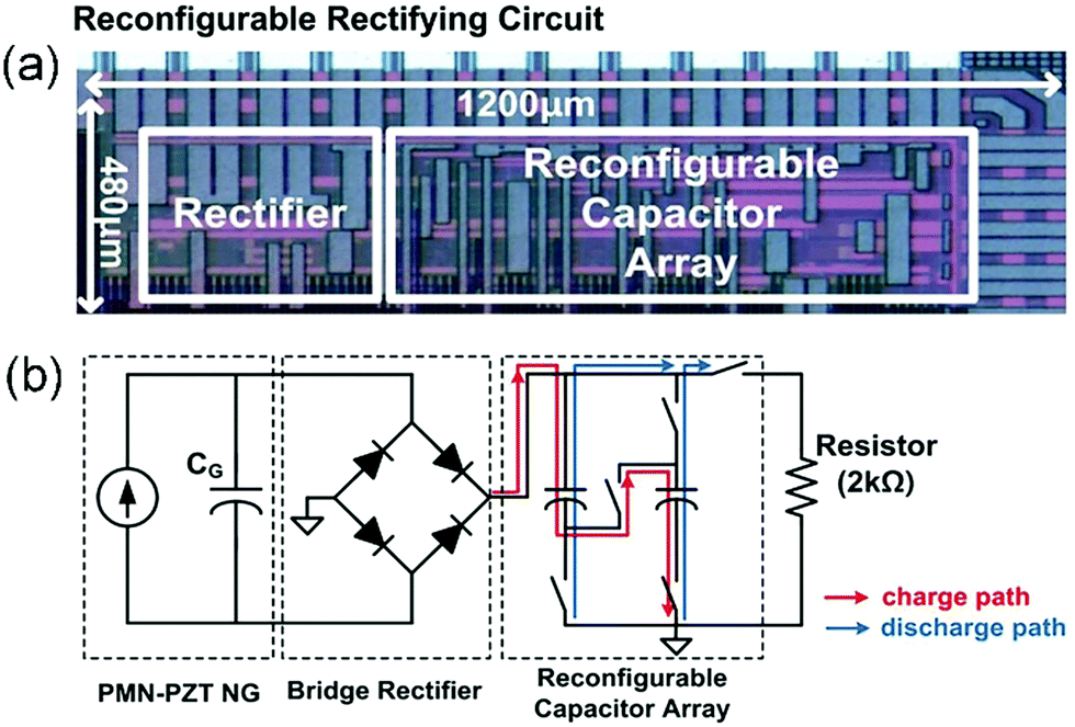 | ||
| Fig. 12 (a) A top-view OM image and (b) schematic circuit diagram of the designed reconfigurable rectifying circuit system integrated with a flexible PMN–PZT energy harvester, bridge rectifier, reconfigurable capacitor charger array, and external load.125 Reprinted with permission from ref. 125. Copyright©2015 Wiley-VCH Verlag GmbH & Co. KGaA, Weinheim. | ||
5. Conclusions
FE devices have been widely applied for transducing energy, monitoring pressure and actuating motors. The successful fabrication of flexible FE films will extend the application of FE materials into the field of flexible electronics, and flexible FE devices will certainly shine in the area of the IoT and robotics. The research on flexible FE devices is on the rise, but most papers report only discrete device components. The most critical issue is how to integrate flexible FE devices with other electronic components. In this article, we have summarized the fabrication methods for producing flexible FE films and highlighted the recent progress made in flexible FE devices. We hope that this review can promote further development and great breakthrough in this intriguing research field.Conflicts of interest
There are no conflicts to declare.Acknowledgements
The work was supported by the National Key R&D Program of China (Grant No. 2018YFB0407601), the Natural Science Foundation of China (Grant No. 51472199, 11534015, 51602244, and 51802248), the National Key Laboratory Foundation (Grant No. 2018SSFNKLSMT-04 and 614241101010117), the Key R&D Program of Shaanxi Province (Grant No. 2018GY-109) and the National 111 Project of China (B14040).References
- Q. Wu, Y. Xu, Z. Yao, A. Liu and G. Shi, ACS Nano, 2010, 4, 1963–1970 CrossRef CAS PubMed.
- G. A. Snook, P. Kao and A. S. Best, J. Power Sources, 2011, 196, 1–12 CrossRef CAS.
- J. Y. Oh, S. Kim, H.-K. Baik and U. Jeong, Adv. Mater., 2016, 28, 4455–4461 CrossRef CAS PubMed.
- A. N. Sokolov, Y. D. Cao, O. B. Johnson and Z. A. Bao, Adv. Funct. Mater., 2012, 22, 175–183 CrossRef CAS.
- Y. M. You, Y. Y. Tang, P. F. Li, H. Y. Zhang, W. Y. Zhang, Y. Zhang, H. Y. Ye, T. Nakamura and R. G. Xiong, Nat. Commun., 2017, 8, 14934 CrossRef CAS PubMed.
- L. Persano, C. Dagdeviren, Y. Su, Y. Zhang, S. Girardo, D. Pisignano, Y. Huang and J. A. Rogers, Nat. Commun., 2013, 4, 1633 CrossRef PubMed.
- M. Owczarek, K. A. Hujsak, D. P. Ferris, A. Prokofjevs, I. Majerz, P. Szklarz, H. Zhang, A. A. Sarjeant, C. L. Stern, R. Jakubas, S. Hong, V. P. Dravid and J. F. Stoddart, Nat. Commun., 2016, 7, 13108 CrossRef CAS PubMed.
- Y. Liu, H. Aziguli, B. Zhang, W. Xu, W. Lu, J. Bernholc and Q. Wang, Nature, 2018, 562, 96–100 CrossRef CAS.
- X. Han, X. Chen, X. Tang, Y.-L. Chen, J.-H. Liu and Q.-D. Shen, Adv. Funct. Mater., 2016, 26, 3640–3648 CrossRef CAS.
- L. Persano, C. Dagdeviren, C. Maruccio, L. D. Lorenzis and D. Pisignano, Adv. Mater., 2014, 26, 7574–7580 CrossRef CAS PubMed.
- S. Lim, D. Son, J. Kim, Y. B. Lee, J.-K. Song, S. Choi, D. J. Lee, J. H. Kim, M. Lee, T. Hyeon and D.-H. Kim, Adv. Funct. Mater., 2015, 25, 375–383 CrossRef CAS.
- T. Sekine, R. Sugano, T. Tashiro, J. Sato, Y. Takeda, H. Matsui, D. Kumaki, F. Domingues Dos Santos, A. Miyabo and S. Tokito, Sci. Rep., 2018, 8, 4442 CrossRef.
- T. Someya, Y. Kato, T. Sekitani, S. Iba, Y. Noguchi, Y. Murase, H. Kawaguchi and T. Sakurai, Proc. Cambridge Philos. Soc., 2005, 102, 12321–12325 CAS.
- S.-H. Bae, O. Kahya, B. K. Sharma, J. Kwon, H. J. Cho, B. Özyilmaz and J.-H. Ahn, ACS Nano, 2013, 7, 3130–3138 CrossRef CAS.
- M. Lee, C.-Y. Chen, S. Wang, S. N. Cha, Y. J. Park, J. M. Kim, L.-J. Chou and Z. L. Wang, Adv. Mater., 2012, 24, 1759–1764 CrossRef CAS.
- Z.-H. Shen, J.-J. Wang, J.-Y. Jiang, Y.-H. Lin, C.-W. Nan, L.-Q. Chen and Y. Shen, Adv. Energy Mater., 2018, 8, 1800509 CrossRef.
- Z.-H. Shen, J.-J. Wang, Y. Lin, C.-W. Nan, L.-Q. Chen and Y. Shen, Adv. Mater., 2018, 30, 1704380 CrossRef.
- X. Zhang, J. Jiang, Z. Shen, Z. Dan, M. Li, Y. Lin, C.-W. Nan, L. Chen and Y. Shen, Adv. Mater., 2018, 30, e1707269 CrossRef.
- X. Zhang, Y. Shen, B. Xu, Q. Zhang, L. Gu, J. Jiang, J. Ma, Y. Lin and C.-W. Nan, Adv. Mater., 2016, 28, 2055–2061 CrossRef CAS.
- Prateek, V. K. Thaku and R. K. Gupta, Chem. Rev., 2016, 116, 4260–4317 CrossRef CAS.
- L. Zhu and Q. Wang, Macromolecules, 2012, 45, 2937–2954 CrossRef CAS.
- X. Chen, X. Han and Q.-D. Shen, Adv. Electron. Mater., 2017, 3, 1600460 CrossRef.
- Z. Pan, L. Yao, J. Zhai, X. Yao and H. Chen, Adv. Mater., 2018, 30, e1705662 CrossRef.
- C. Wan and C. R. Bowen, J. Mater. Chem. A, 2017, 5, 3091–3128 RSC.
- C. Pang, G.-Y. Lee, T.-i. Kim, S. M. Kim, H. N. Kim, S.-H. Ahn and K.-Y. Suh, Nat. Mater., 2012, 11, 795–801 CrossRef CAS.
- S. Xu, Y. Zhang, J. Cho, J. Lee, X. Huang, L. Jia, J. A. Fan, Y. Su, J. Su, H. Zhang, H. Cheng, B. Lu, C. Yu, C. Chuang, T.-i. Kim, T. Song, K. Shigeta, S. Kang, C. Dagdeviren, I. Petrov, P. V. Braun, Y. Huang, U. Paik and J. A. Rogers, Nat. Commun., 2013, 4, 1543 CrossRef.
- M. S. Mannoor, H. Tao, J. D. Clayton, A. Sengupta, D. L. Kaplan, R. R. Naik, N. Verma, F. G. Omenetto and M. C. McAlpine, Nat. Commun., 2012, 3, 763 CrossRef.
- Z. Wang, X. Wang, M. Li, Y. Gao, Z. Hu, T. Nan, X. Liang, H. Chen, J. Yang, S. Cash and N.-X. Sun, Adv. Mater., 2016, 28, 9370–9377 CrossRef CAS.
- S. Hage-Ali, N. Tiercelin, P. Coquet, R. Sauleau, V. Preobrazhensky and P. Pernod, IEEE Antennas and Wireless Propagation Letters, 2010, 9, 1131–1134 Search PubMed.
- B. Zhu, H. Wang, W. R. Leow, Y. Cai, X. J. Loh, M.-Y. Han and X. Chen, Adv. Mater., 2016, 28, 4250–4265 CrossRef CAS PubMed.
- Q. Yang, Z. Zhou, L. Wang, H. Zhang, Y. Cheng, Z. Hu, B. Peng and M. Liu, Adv. Mater., 2018, 30, 1800449 CrossRef.
- M. L. Hammock, A. Chortos, B. C. K. Tee, J. B. H. Tok and Z. Bao, Adv. Mater., 2013, 25, 5997–6038 CrossRef CAS.
- A. Chortos, J. Liu and Z. Bao, Nat. Mater., 2016, 15, 937–950 CrossRef CAS PubMed.
- J. Heikenfeld, A. Jajack, J. Rogers, P. Gutruf, L. Tian, T. Pan, R. Li, M. Khine, J. Kim, J. Wang and J. Kim, Lab Chip, 2018, 18, 217–248 RSC.
- T. Q. Trung and N.-E. Lee, Adv. Mater., 2016, 28, 4338–4372 CrossRef CAS.
- Y. H. Do, M. G. Kang, J. S. Kim, C. Y. Kang and S. J. Yoon, Sens. Actuators, A, 2012, 184, 124–127 CrossRef CAS.
- C. K. Jeong, S. B. Cho, J. H. Han, D. Y. Park, S. Yang, K.-I. Park, J. Ryu, H. Sohn, Y.-C. Chung and K. J. Lee, Nano Res., 2016, 10, 437–455 CrossRef.
- C. K. Jeong, J. H. Han, H. Palneedi, H. Park, G.-T. Hwang, B. Joung, S.-G. Kim, H. J. Shin, I.-S. Kang, J. Ryu and K. J. Lee, APL Mater., 2017, 5, 074102 CrossRef.
- C. K. Jeong, K.-I. Park, J. H. Son, G.-T. Hwang, S. H. Lee, D. Y. Park, H. E. Lee, H. K. Lee, M. Byun and K. J. Lee, Energy Environ. Sci., 2014, 7, 4035–4043 RSC.
- H. S. Lee, J. Chung, G.-T. Hwang, C. K. Jeong, Y. Jung, J.-H. Kwak, H. Kang, M. Byun, W. D. Kim, S. Hur, S.-H. Oh and K. J. Lee, Adv. Funct. Mater., 2014, 24, 6914–6921 CrossRef CAS.
- D. Y. Park, D. J. Joe, D. H. Kim, H. Park, J. H. Han, C. K. Jeong, H. Park, J. G. Park, B. Joung and K. J. Lee, Adv. Mater., 2017, 29, 1702308 CrossRef.
- Z. L. Wang and J. Song, Science, 2006, 312, 242–246 CrossRef CAS PubMed.
- T. Amrillah, Y. Bitla, K. Shin, T. Yang, Y.-H. Hsieh, Y.-Y. Chiou, H.-J. Liu, T. H. Do, D. Su, Y.-C. Chen, S.-U. Jen, L.-Q. Chen, K. H. Kim, J.-Y. Juang and Y.-H. Chu, ACS Nano, 2017, 11, 6122–6130 CrossRef CAS.
- W. C. Zheng, D. X. Zheng, Y. C. Wang, D. Li, C. Jin and H. L. Bai, J. Magn. Magn. Mater., 2019, 481, 227–233 CrossRef CAS.
- G. Dong, Z. Zhou, M. Guan, X. Xue, M. Chen, J. Ma, Z. Hu, W. Ren, Z.-G. Ye, C.-W. Nan and M. Liu, ACS Nano, 2018, 12, 3751–3758 CrossRef CAS.
- G. Dong, Z. Zhou, X. Xue, Y. Zhang, B. Peng, M. Guan, S. Zhao, Z. Hu, W. Ren, Z. G. Ye and M. Liu, ACS Appl. Mater. Interfaces, 2017, 9, 30733–30740 CrossRef CAS.
- J.-F. Ge, Z.-L. Liu, C. Liu, C.-L. Gao, D. Qian, Q.-K. Xue and J.-F. Jia, Nat. Mater., 2015, 14, 285–289 CrossRef CAS PubMed.
- R. M. Lutchyn, J. D. Sau and D. S. Das, Phys. Rev. Lett., 2010, 105, 077001 CrossRef PubMed.
- V. Mourik, K. Zuo, S. M. Frolov, S. R. Plissard, E. P. A. M. Bakkers and L. P. Kouwenhoven, Science, 2012, 336, 1003–1007 CrossRef CAS PubMed.
- Y. Bitla, C. Chen, H.-C. Lee, T. H. Do, C.-H. Ma, L. V. Qui, C.-W. Huang, W.-W. Wu, L. Chang, P.-W. Chiu and Y.-H. Chu, ACS Appl. Mater. Interfaces, 2016, 8, 32401–32407 CrossRef CAS PubMed.
- C.-I. Li, J.-C. Lin, H.-J. Liu, M.-W. Chu, H.-W. Chen, C.-H. Ma, C.-Y. Tsai, H.-W. Huang, H.-J. Lin, H.-L. Liu, P.-W. Chiu and Y.-H. Chu, Chem. Mater., 2016, 28, 3914–3919 CrossRef CAS.
- J. Liu, Y. Feng, R. Tang, R. Zhao, J. Gao, D. Shi and H. Yang, Adv. Electron. Mater., 2018, 4, 1700522 CrossRef.
- S.-E. Park and T. R. Shrout, J. Appl. Phys., 1997, 82, 1804–1811 CrossRef CAS.
- Z.-G. Ye, MRS Bull., 2011, 34, 277–283 CrossRef.
- J. Deng, Y. Liu, J. Liu, D. Xu and Y. Wang, IEEE Trans. Ind. Electron., 2019, 66, 6141–6149 Search PubMed.
- F. Li, M. J. Cabral, B. Xu, Z. Cheng, E. C. Dickey, J. M. LeBeau, J. Wang, J. Luo, S. Taylor, W. Hackenberger, L. Bellaiche, Z. Xu, L.-Q. Chen, T. R. Shrout and S. Zhang, Science, 2019, 364, 264–268 CrossRef CAS PubMed.
- J. Rödel, K. G. Webber, R. Dittmer, W. Jo, M. Kimura and D. Damjanovic, J. Eur. Ceram. Soc., 2015, 35, 1659–1681 CrossRef.
- V. Garcia and M. Bibes, Nat. Commun., 2014, 5, 4289 CrossRef CAS PubMed.
- H. Lu, A. Lipatov, S. Ryu, D. J. Kim, H. Lee, M. Y. Zhuravlev, C. B. Eom, E. Y. Tsymbal, A. Sinitskii and A. Gruverman, Nat. Commun., 2014, 5, 5518 CrossRef CAS PubMed.
- E. Mikheev, B. D. Hoskins, D. B. Strukov and S. Stemmer, Nat. Commun., 2014, 5, 3990 CrossRef CAS PubMed.
- Y. Qi and M. C. McAlpine, Energy Environ. Sci., 2010, 3, 1275 RSC.
- K.-I. Park, J. H. Son, G.-T. Hwang, C. K. Jeong, J. Ryu, M. Koo, I. Choi, S. H. Lee, M. Byun, Z. L. Wang and K. J. Lee, Adv. Mater., 2014, 26, 2514–2520 CrossRef CAS PubMed.
- W. S. Wong, T. Sands and N. W. Cheung, Appl. Phys. Lett., 1998, 72, 599–601 CrossRef CAS.
- Y. Chen, Y. Zhang, F. Yuan, F. Ding and O. G. Schmidt, Adv. Electron. Mater., 2017, 3, 1600540 CrossRef.
- G. Dong, S. Li, M. Yao, Z. Zhou, Y. Q. Zhang, X. Han, Z. Luo, J. Yao, B. Peng, Z. Hu, H. Huang, T. Jia, J. Li, W. Ren, Z. G. Ye, X. Ding, J. Sun, C. W. Nan, L. Q. Chen, J. Li and M. Liu, Science, 2019, 366, 475–479 CrossRef CAS PubMed.
- C. Dagdeviren, Y. Shi, P. Joe, R. Ghaffari, G. Balooch, K. Usgaonkar, O. Gur, P. L. Tran, J. R. Crosby, M. Meyer, Y. Su, R. Chad Webb, A. S. Tedesco, M. J. Slepian, Y. Huang and J. A. Rogers, Nat. Mater., 2015, 14, 728–736 CrossRef CAS PubMed.
- J. Jiang, Y. Bitla, C.-W. Huang, T. H. Do, H.-J. Liu, Y.-H. Hsieh, C.-H. Ma, C.-Y. Jang, Y.-H. Lai, P.-W. Chiu, W.-W. Wu, Y.-C. Chen, Y.-C. Zhou and Y.-H. Chu, Sci. Adv., 2017, 3, e1700121 CrossRef PubMed.
- K.-I. Park, M. Lee, Y. Liu, S. Moon, G.-T. Hwang, G. Zhu, J. E. Kim, S. Ouk Kim, D. K. Kim, Z. L. Wang and K. J. Lee, Adv. Mater., 2012, 24, 2999–3004 CrossRef CAS PubMed.
- W. Lee, O. Kahya, C. T. Toh, B. Özyilmaz and J.-H. Ahn, Nanotechnology, 2013, 24, 475202 CrossRef PubMed.
- C. K. Jeong, I. Kim, K.-I. Park, M. H. Oh, H. Paik, G.-T. Hwang, K. No, Y. S. Nam and K. J. Lee, ACS Nano, 2013, 7, 11016–11025 CrossRef CAS PubMed.
- K.-I. Park, C. K. Jeong, J. Ryu, G.-T. Hwang and K. J. Lee, Adv. Energy Mater., 2013, 3, 1539–1544 CrossRef CAS.
- K. Cung, B. J. Han, T. D. Nguyen, S. Mao, Y.-W. Yeh, S. Xu, R. R. Naik, G. Poirier, N. Yao, P. K. Purohit and M. C. McAlpine, Nano Lett., 2013, 13, 6197–6202 CrossRef CAS.
- C. K. Jeong, K.-I. Park, J. Ryu, G.-T. Hwang and K. J. Lee, Adv. Funct. Mater., 2014, 24, 2620–2629 CrossRef CAS.
- S. Xu, Y.-w. Yeh, G. Poirie, M. C. McAlpine, R. A. Register and N. Yao, Nano Lett., 2013, 13, 2393–2398 CrossRef CAS PubMed.
- L. Gu, N. Cui, L. Cheng, Q. Xu, S. Bai, M. Yuan, W. Wu, L. Jinmei, Y. Zhao, F. Ma, Y. Qin and Z. L. Wang, Nano Lett., 2013, 13, 91–94 CrossRef CAS PubMed.
- C. Chang, V. H. Tran, J. Wang, Y. K. Fuh and L. Lin, Nano Lett., 2010, 10, 726–731 CrossRef CAS PubMed.
- Y. Hu, Y. Zhang, C. Xu, L. Lin, R. L. Snyder and Z. L. Wang, Nano Lett., 2011, 11, 2572–2577 CrossRef CAS.
- K.-I. Park, S. Xu, Y. Liu, G.-T. Hwang, S.-J. L. Kang, Z. L. Wang and K. J. Lee, Nano Lett., 2010, 10, 4939–4943 CrossRef CAS PubMed.
- C. Dagdeviren, Y. Su, P. Joe, R. Yona, Y. Liu, Y.-S. Kim, Y. Huang, A. R. Damadoran, J. Xia, L. W. Martin, Y. Huang and J. A. Rogers, Nat. Commun., 2014, 5, 4496 CrossRef CAS PubMed.
- C. Dagdeviren, B. D. Yang, Y. Su, P. L. Tran, P. Joe, E. Anderson, J. Xia, V. Doraiswamy, B. Dehdashti, X. Feng, B. Lu, R. Poston, Z. Khalpey, R. Ghaffari, Y. Huang, M. J. Slepian and J. A. Rogers, Proc. Natl. Acad. Sci. U. S. A., 2014, 111, 1927–1932 CrossRef CAS.
- S. R. Bakaul, C. R. Serrao, M. Lee, C. W. Yeung, A. Sarker, S.-L. Hsu, A. K. Yadav, L. Dedon, L. You, A. I. Khan, J. D. Clarkson, C. Hu, R. Ramesh and S. Salahuddin, Nat. Commun., 2016, 7, 10547 CrossRef CAS.
- Y. Zhang, L. Shen, M. Liu, X. Li, X. Lu, L. Lu, C. Ma, C. You, A. Chen, C. Huang, L. Chen, M. Alexe and C. L. Jia, ACS Nano, 2017, 11, 8002–8009 CrossRef CAS.
- W. S. Wong, T. Sands, N. W. Cheung, M. Kneissl, D. P. Bour, P. Mei, L. T. Romano and N. M. Johnson, Appl. Phys. Lett., 1999, 75, 1360–1362 CrossRef CAS.
- R. Maeda, J. J. Tsaur, S. H. Lee and M. Ichiki, J. Electroceram., 2004, 12, 89–100 CrossRef.
- M. S. Zarnik, D. Belavič, S. Maček and J. Holc, Int. J. Appl. Ceram. Technol., 2009, 6, 9–17 CrossRef CAS.
- J. Soman and C. B. O'Neal, IEEE Sens. J., 2011, 11, 78–85 Search PubMed.
- A. Koma, J. Cryst. Growth, 1999, 201, 236–241 CrossRef.
- A. Koma, Thin Solid Films, 1992, 72–76 CrossRef CAS.
- A. Koma, K. Ueno and K. Saiki, J. Cryst. Growth, 1991, 1029–1032 CrossRef CAS.
- Y.-H. Chu, npj Quantum Mater., 2017, 2, 1–5 CrossRef.
- P.-C. Wu and Y.-H. Chu, J. Mater. Chem. C, 2018, 6, 6102–6117 RSC.
- Y. Bitla and Y.-H. Chu, FlatChem, 2017, 3, 26–42 CrossRef CAS.
- Y. He, H. Dong, Q. Meng, L. Jiang, W. Shao, L. He and W. Hu, Adv. Mater., 2011, 23, 5502–5507 CrossRef CAS.
- W. Gao, L. You, Y. Wang, G. Yuan, Y.-H. Chu, Z. Liu and J.-M. Liu, Adv. Electron. Mater., 2017, 3, 1600542 CrossRef.
- C. Yang, Y. Han, J. Qian and Z. Cheng, Adv. Electron. Mater., 2019, 5, 1900443 CrossRef CAS.
- C.-H. Ma, J.-C. Lin, H.-J. Liu, T. H. Do, Y.-M. Zhu, T. D. Ha, Q. Zhan, J.-Y. Juang, Q. He, E. Arenholz, P.-W. Chiu and Y.-H. Chu, Appl. Phys. Lett., 2016, 108, 253104 CrossRef.
- H.-J. Liu, C.-K. Wang, D. Su, T. Amrillah, Y.-H. Hsieh, K.-H. Wu, Y.-C. Chen, J.-Y. Juang, L. M. Eng, S.-U. Jen and Y.-H. Chu, ACS Appl. Mater. Interfaces, 2017, 9, 7297–7304 CrossRef CAS.
- W. Liu, M. Liu, R. Ma, R. Zhang, W. Zhang, D. Yu, Q. Wang, J. Wang and H. Wang, Adv. Funct. Mater., 2018, 28, 1705928 CrossRef.
- A. K. Geim and I. V. Grigorieva, Nature, 2013, 499, 419–425 CrossRef CAS.
- T. D. Nguyen, N. Deshmukh, J. M. Nagarah, T. Kramer, P. K. Purohit, M. J. Berry and M. C. McAlpine, Nat. Nanotechnol., 2012, 7, 587–593 CrossRef CAS.
- C. Dagdeviren, F. Javid, S. Saxton, C. Cleveland, R. Langer, P. Joe and G. Traverso, Nat. Biomed. Eng., 2017, 1, 807–817 CrossRef CAS.
- G. T. Hwang, H. Park, J. H. Lee, S. Oh, K. I. Park, M. Byun, H. Park, G. Ahn, C. K. Jeong, K. No, H. Kwon, S. G. Lee, B. Joung and K. J. Lee, Adv. Mater., 2014, 26, 4880–4887 CrossRef CAS PubMed.
- G.-T. Hwang, Y. Kim, J.-H. Lee, S. Oh, C. K. Jeong, D. Y. Park, J. Ryu, H. Kwon, S.-G. Lee, B. Joung, D. Kim and K. J. Lee, Energy Environ. Sci., 2015, 8, 2677–2684 RSC.
- Z. Li, G. Zhu, R. Yang, A. C. Wang and Z. L. Wang, Adv. Mater., 2010, 22, 2534–2537 CrossRef CAS.
- T. Inaoka, H. Shintaku, T. Nakagawa, S. Kawano, H. Ogita, T. Sakamoto, S. Hamanishi, H. Wada and J. Ito, Proc. Natl. Acad. Sci. U. S. A., 2011, 108, 18390–18395 CrossRef CAS.
- M. R. Sohail, D. Z. Uslan, A. H. Khan, P. A. Friedman, D. L. Hayes, W. R. Wilson, J. M. Steckelberg, S. Stoner and L. M. Baddour, J. Am. Coll. Cardiol., 2007, 49, 1851–1859 CrossRef.
- M. J. Wilhelm, C. Schmid, D. Hammel, S. Kerber, H. M. Loick, M. Herrmann and H. H. Scheld, Ann. Thorac. Surg., 1997, 64, 1707–1712 CrossRef CAS PubMed.
- F. W. Horlbeck, F. Mellert, J. Kreuz, G. Nickenig and J. O. Schwab, J. Cardiovasc. Electrophysiol., 2012, 23, 1336–1342 CrossRef PubMed.
- A. J. Fenoy and R. K. Simpson, Jr, J. Neurosurg., 2014, 120, 132–1399 Search PubMed.
- Y. Hu, L. Lin, Y. Zhang and Z. L. Wang, Adv. Mater., 2012, 24, 110–114 CrossRef CAS.
- Y. Khan, A. E. Ostfeld, C. M. Lochner, A. Pierre and A. C. Arias, Adv. Mater., 2016, 28, 4373–4395 CrossRef CAS.
- S. Breit, J. B. Schulz and A. L. Benabid, Cell Tissue Res., 2004, 318, 275–288 CrossRef.
- A. S. Meidert and B. Saugel, Front. Med., 2018, 4, 231 CrossRef.
- A. Stenglova and J. Benes, Front. Med., 2017, 4, 202 CrossRef.
- C. Li, G. Guan, R. Reif, Z. Huang and R. K. Wang, J. R. Soc., Interface, 2012, 9, 831–841 CrossRef.
- D. Bommannan, R. O. Potts and R. H. Guy, J. Invest. Dermatol., 1990, 95, 403–408 CrossRef CAS.
- M. J. Paszek, N. Zahir, K. R. Johnson, J. N. Lakins, G. I. Rozenberg, A. Gefen, C. A. Reinhart-King, S. S. Margulies, M. Dembo, D. Boettiger, D. A. Hammer and V. M. Weaver, Cancer Cell, 2005, 8, 241–254 CrossRef CAS PubMed.
- Q. Zheng, B. Shi, Z. Li and Z. L. Wang, Adv. Sci., 2017, 4, 1700029 CrossRef.
- X. Chen, S. Xu, N. Yao and Y. Shi, Nano Lett., 2010, 10, 2133–2137 CrossRef CAS.
- Y. Qi, N. T. Jafferis, K. Lyons, Jr., C. M. Lee, H. Ahmad and M. C. McAlpine, Nano Lett., 2010, 10, 524–528 CrossRef CAS PubMed.
- Y. Qi, J. Kim, T. D. Nguyen, B. Lisko, P. K. Purohit and M. C. McAlpine, Nano Lett., 2011, 11, 1331–1336 CrossRef CAS PubMed.
- J. Kwon, W. Seung, B. K. Sharma, S. W. Kim and J. H. Ahn, Energy Environ. Sci., 2012, 5, 8970–8975 RSC.
- S. H. Shin, Y. H. Kim, M. H. Lee, J. Y. Jung and J. Nah, ACS Nano, 2014, 8, 2766–2773 CrossRef CAS.
- J. Yang, J. Kim and S. Lee, Electron. Lett., 2014, 50, 629–631 CrossRef.
- G.-T. Hwang, J. Yang, S. H. Yang, H.-Y. Lee, M. Lee, D. Y. Park, J. H. Han, S. J. Lee, C. K. Jeong, J. Kim, K.-I. Park and K. J. Lee, Adv. Energy Mater., 2015, 5, 1500051 CrossRef.
Footnote |
| † These authors contributed equally. |
| This journal is © The Royal Society of Chemistry 2020 |