
 Open Access Article
 This Open Access Article is licensed under a Creative Commons Attribution-Non Commercial 3.0 Unported Licence
Rapid hybrid chemical vapor deposition for efficient and hysteresis-free perovskite solar modules with an operation lifetime exceeding 800 hours†
Longbin
Qiu‡
 ,
Sisi
He‡
,
Zonghao
Liu
,
Luis K.
Ono
,
Dae-Yong
Son
,
Yuqiang
Liu
,
Guoqing
Tong
and
Yabing
Qi
*
,
Sisi
He‡
,
Zonghao
Liu
,
Luis K.
Ono
,
Dae-Yong
Son
,
Yuqiang
Liu
,
Guoqing
Tong
and
Yabing
Qi
*
Energy Materials and Surface Sciences Unit (EMSSU), Okinawa Institute of Science and Technology Graduate University (OIST), 1919-1 Tancha, Kunigami-gun, Onna-son, Okinawa 904-0495, Japan. E-mail: Yabing.Qi@OIST.jp
First published on 20th October 2020
Abstract
Hybrid chemical vapor deposition (HCVD) has been employed in the fabrication of perovskite solar cells (PSCs) and modules (PSMs), and it shows strong promise for upscalable fabrication. The conventional HCVD process needs a relatively long processing time (e.g., several hours) and the fabricated PSCs often exhibit salient hysteresis, which impedes utilization of this technology for mass production. Herein, we demonstrate a rapid HCVD (RHCVD) fabrication process for PSCs using a rapid thermal process, which not only significantly reduces the deposition time to less than 10 min, but also effectively suppresses hysteresis. This markedly reduced deposition time is comparable to that of solution-coating processes. Furthermore, the shorter processing time inside the furnace reduces the exposure time of the glass/ITO/SnO2 substrates under vacuum, which helps maintain the high quality of the SnO2 electron-transport layer and results in a lower density of gap states. Finally, PSMs with a designated area of 22.4 cm2 fabricated via RHCVD achieved an efficiency of 12.3%, and maintained 90% of the initial value after operation under continuous light illumination for over 800 h.
Introduction
Perovskite, as a low-cost material, has boosted the performance up to 25.2% for small area (0.09 cm2) single-junction solar cells1 and the expected levelized cost of electricity (LCOE) is as low as 3.5 US cents per kW h (for comparison, the LCOE for grid power is 7.04–11.90 US cents per kW h and for c-Si solar cells it is 9.78–19.33 US cents per kW h) when assuming a 1 m2 module with 20% efficiency and >15 years lifetime,2,3 and this exceeds the 2030 goals of the US Department of Energy of 5 US cents per kW h for residential solar power.4 Recently, there has been more and more work focused on upscalable fabrication of perovskite solar modules (PSMs) to transfer the desired performance from small area cells to large-area modules.5 However, there is still a large gap between small area cells and large-area modules.5 To achieve upscalable fabrication, a key indicator is the performance decay rate upon upscaling. For mature photovoltaic technologies (e.g., crystalline silicon solar cells, polycrystalline silicon solar cells, CdTe solar cells), the absolute performance decay rate is around 0.8% per decade of the area increase.6,7 If the same decay rate can be realized for perovskite photovoltaic technologies, a power conversion efficiency (PCE) of approximately 22% would be expected for a module with an area of approximately 1000 cm2 when scaling up from the state of the art small area cells (25.2% PCE with a cell area of 0.0937 cm2).6 Currently the highest reported PCE for such a large-size PSM is 17.9% with a designated area of 804 cm2.1 To reduce the large PCE gap between small area cells and large-area modules, upscalable fabrication methods for the perovskite and other functional layers (e.g., electron transport layer (ETL), hole transport layer (HTL), electrode and interface modification) are required.5 For the upscalable fabrication of perovskite solar cells (PSCs), both solution- and vapor-based processes have been reported, including doctor blading,8,9 slot-die coating,10 spray coating,11 thermal evaporation12 and hybrid chemical vapor deposition (HCVD).5,13,14HCVD is a promising method as compared to the solution-based ones because of its advantages, such as uniform deposition across large areas, low cost, solvent-free, and readiness for integration with other thin film solar technologies (e.g., thin film silicon solar cells) to form tandem solar cells.13 Currently, the decay rate between small area solar cells and large area solar modules upon upscaling is 1.3% per decade of the area increase,15 which is approaching other mature photovoltaic technologies. HCVD is a two-step deposition process. In the first step, inorganic precursor materials (e.g., PbI2, PbCl2, CsI, etc.) are deposited by thermal evaporation,14 spray coating13 or spin coating.16 In the second step, organic precursor materials (e.g., FAI, MAI, MABr, etc., where FA is formamidinium and MA is methylammonium) are sublimed in the first heating zone of a CVD tube furnace, and subsequently driven by a gas flow (e.g., dry N2, Ar, or dry air) towards the second heating zone, where the organic precursor vapor reacts with the inorganic precursor that is pre-deposited on the substrate, leading to perovskite film growth.14,15 Based on the pressure and heating zone temperatures, a variety of HCVD techniques can be developed to fabricate perovskite films, including atmospheric pressure HCVD,16–18 low-pressure HCVD,14 single-zone HCVD19,20 and double-zone HCVD.14 However, all of the HCVD processes usually need a relatively long processing time (2–3 hours), which severely limits their mass-production capabilities for solar cell fabrication. Reducing the deposition time is still a challenge that needs to be fully addressed for the further development of the module-scale HCVD technique. Furthermore, it has been found that the long deposition time has a detrimental effect on the ETL, such as SnO2 or TiO2, which deteriorates the solar module performance.15 Also, hysteresis was observed due to the un-optimized interface between this ETL layer and the perovskite layer. Incorporation of an additional buffer layer such as C60 improves the HCVD processed solar cell performance by reducing the negative impact of vacuum annealing on the ETL.15 However, this additional layer increases the cost and complexity of the deposition process.
Herein, we report a rapid HCVD (RHCVD) process to fabricate PSCs and PSMs (Fig. 1). The RHCVD process greatly reduces the deposition time from several hours to within 10 min, which is comparable with typical solution coating processes. As compared with the regular HCVD process, the RHCVD processed PSCs exhibits only slight hysteresis even without any additional interfacial buffer layer. Using RHCVD, we obtained an efficiency of 15.5% for the small-area PSC (active area = 0.1 cm2). Furthermore, we show that the RHCVD process is readily upscalable for fabricating PSMs, the area of which is only limited by the size of the CVD tube furnace. As a demonstration, we fabricated PSMs on 5 cm by 5 cm substrates with a designated area of 22.4 cm2 and a geometric fill factor of approximately 90%. The performance of the PSMs was up to 12.3% with almost no hysteresis. The 224 times increase in the device area with an absolute PCE reduction of 3.2% (i.e., a decay rate of 1.36% per decade of the area increase), further confirms the upscalability of this RHCVD method. The operational lifetime of the encapsulated PSMs was tested under continuous light illumination with a steady voltage output (the initial maximum power point (MPP) voltage) and the PSM maintained 90% of its initial performance after operation for more than 800 h.
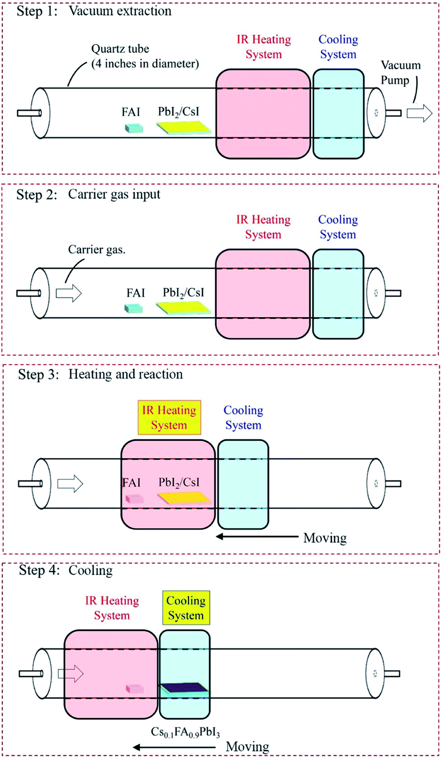 | ||
| Fig. 1 Schematic illustrations showing the steps and major features for fabricating perovskite films via the RHCVD method. Step 1: the loading of a crucible containing the organic compound and solar module substrate(s) with the pre-coated inorganic layer into a single-zone quartz tube. Step 2: flowing of the carrier gas (e.g., dry N2, Ar, air, etc.), keeping the vacuum at a pressure of 10 Torr. Step 3: sliding the IR heating system to enclose both the organic powder and substrate and followed by the starting the IR heating system. Step 4: after the heating process is finished, the IR heating system is turned off and the cooling system is turned on. The cooling system is slid to the substrate position. | ||
Results and discussion
In this work, we used an n–i–p planar PSC structure with the perovskite layer sandwiched between the ETL and HTL, which is a simple structure without the mesoporous structures.21 This structure also eliminates the high-temperature step needed to process mesoporous structures, which helps reduce cost. Fig. 2a displays the structure of the PSC with the configuration of ITO/SnO2/perovskite/spiro-MeOTAD/Au, in which the perovskite layer is deposited by RHCVD with a composition of Cs0.1FA0.9PbI3. A small amount of Cs cations is added to improve the phase stability of FAPbI3.22,23 Similar to the regular HCVD process, the RHCVD process is a two-step process with the first step consisting of co-evaporation of CsI and PbI2 by optimizing the deposition rates to realize the desired composition.5,15 In the second step, the substrates pre-coated with the mixture film of CsI and PbI2 are placed in a CVD tube furnace to react with FAI to form perovskite. On the basis of the temperature profile (for the heating zone containing the substrates) as a function of time shown in Fig. 2b, in a regular HCVD process the total deposition time of FAI is approximately 230 min (the temperature ramping time is 65 min and the deposition time is 160 min, with about 5 min of cooling down when the furnace cap is opened to speed up dropping of the temperature to below 100 °C) to ensure the complete conversion of PbI2 to perovskite.15,19,20 The temperature profile for the heating zone containing the organic precursor is shown in Fig. S1.† The temperature ramping rate is slow, e.g., 2.3 °C min−1 to obtain stable ramping for a relatively low annealing temperature. Setting higher ramping rates (e.g., 5 °C min−1) can lead to uncontrollable temperature fluctuations. For example, when a fast temperature ramping is used, the actual temperature in the CVD tube can reach much higher temperatures than the programmed temperature (Fig. S2†), which may lead to damage of the perovskite layer. We developed a single zone RHCVD process using a rapid-thermal annealing (RTA) tube furnace. The RTA tube furnace uses an infrared (IR) heating component to achieve ultrafast temperature ramping. The IR heating component is mechanically movable along the furnace tube, which enables fast heating and cooling. The RHCVD process for the deposition of perovskite is less than 10 min (Fig. 2b). Detailed steps of the RHCVD process for the deposition of perovskite films are depicted in Fig. 1. Although a similar process was reported previously for the growth of graphene,24 our work is the first report to apply this process for the fabrication of PSCs. | ||
| Fig. 2 (a) A schematic drawing showing the PSC structure. (b) The programmed temperature profile as a function of time during RHCVD and the regular HCVD process for the heating zone containing the substrates. (c) SEM micrograph of the perovskite film prepared by RHCVD. (d) XRD patterns of the perovskite films prepared by RHCVD and regular HCVD. | ||
The as-deposited Cs0.1FA0.9PbI3 film shows a smooth surface and grain sizes in the range of 300–500 nm (Fig. 2c). SEM micrographs confirm the good uniformity of the surface morphology of the RHCVD deposited perovskite films across a relatively large area (20 μm × 13 μm) (Fig. S3†). The XRD result confirms the full conversion of PbI2 to perovskite, as there is a strong peak at 14.0° and no observable peak at 12.7° (Fig. 2d). The smooth baseline and the absence of the peak at around 11.6° indicate that the formed perovskite film is mainly pure α-phase. High resolution Cs 3d core-level X-ray photoelectron spectroscopy (XPS) data verify the incorporation of Cs cations into the perovskite (Fig. S4†), which agrees well with our previous study on the Cs0.1FA0.9PbI2.9Br0.1 perovskite film prepared by the regular HCVD method.15 The composition ratio between Cs and Pb is determined by XPS to be approximately 1![[thin space (1/6-em)]](https://www.rsc.org/images/entities/char_2009.gif) :10, which agrees well with the desired ratio. Our previous studies suggest that iodide (I−) can easily desorb from iodide-based perovskite films leading to generation of iodine (I2) gas under vacuum conditions and subsequently being pumped out.25,26 During the HCVD or RHCVD processes, the large amount of the organic precursor FAI in the crucible (0.1 g) provides sufficient supply of I−, minimizing the deterioration of the perovskite films during the RHCVD process. Furthermore, the fact that perovskite films prepared by RHCVD show high quality and uniformity over a large area (even without additional annealing as compared to most solution processed perovskite films) indicates that RHCVD is an efficient way to form perovskite films, possibly thanks to the dual function of IR heating in promoting perovskite formation, as well as uniformly heating the converted perovskite films to enhance the film crystallinity. The electronic structures of the deposited perovskite Cs0.1FA0.9PbI3 film has been further investigated by UPS (Fig. S5†). The deposited perovskite showed an n-type nature with a work function of 3.92 eV and valence band maximum of 1.50 eV below the Fermi level. The absorbance of the perovskite film has been characterized by UV-vis absorption measurements and the optical band gap of 1.56 eV is determined on the basis of the Tauc-plot (Fig. S6†).
:10, which agrees well with the desired ratio. Our previous studies suggest that iodide (I−) can easily desorb from iodide-based perovskite films leading to generation of iodine (I2) gas under vacuum conditions and subsequently being pumped out.25,26 During the HCVD or RHCVD processes, the large amount of the organic precursor FAI in the crucible (0.1 g) provides sufficient supply of I−, minimizing the deterioration of the perovskite films during the RHCVD process. Furthermore, the fact that perovskite films prepared by RHCVD show high quality and uniformity over a large area (even without additional annealing as compared to most solution processed perovskite films) indicates that RHCVD is an efficient way to form perovskite films, possibly thanks to the dual function of IR heating in promoting perovskite formation, as well as uniformly heating the converted perovskite films to enhance the film crystallinity. The electronic structures of the deposited perovskite Cs0.1FA0.9PbI3 film has been further investigated by UPS (Fig. S5†). The deposited perovskite showed an n-type nature with a work function of 3.92 eV and valence band maximum of 1.50 eV below the Fermi level. The absorbance of the perovskite film has been characterized by UV-vis absorption measurements and the optical band gap of 1.56 eV is determined on the basis of the Tauc-plot (Fig. S6†).
Our solar cells are based on the perovskite films deposited by RHCVD and the SnO2 ETL. In our previous work, the SnO2 ETL was fabricated by sputtering at room temperature.27 The crystallinity of the sputtered SnO2 films was studied as a function of the post-annealing temperature in the range of 100–500 °C. The room temperature deposited SnO2 film showed an amorphous structure, and the crystallinity was only observed after post-annealing at temperatures over 300 °C.27 However, the post-annealing process also deteriorated the quality of the SnO2 films.27 Similar to the reports of Park and coworkers, annealing of the amorphous SnO2 ETL at 500 °C crystallizes SnO2. However, the enhanced crystallinity reduces the device performance and leads to large hysteresis, due to the increased interface capacitance.28 Furthermore, the vacuum annealing process during the regular HCVD process not only damages the deposited SnO2 films, but also increases the density of gap states located between the valence band and Fermi level, which might further decrease the performance of the as-prepared solar cell devices.15 On the other hand, the solution processed films using SnO2 nanocrystal solutions exhibit a higher quality compared with sputtered amorphous SnO2 films after a similar vacuum annealing process in a CVD tube furnace.15 In this work, we performed a detailed study to investigate the influence of the sputtered amorphous SnO2 (i.e., without post-annealing to avoid damage) and solution-processed SnO2 films on the PSC device performance.29,30 First, a nanocrystal SnO2 layer was prepared by spin coating, or alternatively, an amorphous SnO2 layer was prepared by sputter coating on the ITO/glass substrates. The surface morphology of the SnO2 film was first characterized by atomic force microscopy (AFM). As can be seen in Fig. S7,† the solution processed nanocrystal SnO2 film shows a smoother morphology compared with the sputtered SnO2 film. The surface roughness (RMS) for the sputtered SnO2 and solution coated nanocrystal SnO2 films is 2.79 and 0.88 nm, respectively (Fig. S7†). The RMS of the sputtered amorphous SnO2 layer is similar to that of the ITO substrate (2.45 nm) due to a conformal coating, while the SnO2 nanocrystals help reduce the surface roughness of the substrate.27
The PCE for the PSC device based on the spin coated SnO2 nanocrystal ETL is 15.0% in the reverse scan and 14.1% in the forward scan (Fig. S8†). Comparing the PCEs from the reverse scans, the PSC devices have negligible differences based on solution coated SnO2 and sputter deposited SnO2. However, the PSC devices with a sputter-deposited SnO2 ETL showed 7 times higher hysteresis index (0.06 versus 0.41; hysteresis index = (PCEreverse − PCEforward)/PCEreverse) and 57.4% lower forward scan efficiency. The severe hysteresis issue in the PSC devices can be attributed to the sputtered SnO2 ETL that has a combination of an amorphous structure, high surface roughness and a large defect density.27–29 Hence, we selected solution coated SnO2 nanocrystal films as the ETL to fabricate subsequent PSC devices.
We have further studied the advantages of RHCVD compared with the regular HCVD process. The most significant advantage is the much shorter deposition time thanks to the rapid thermal process. RHCVD can lead to increased throughput and hence lower cost. It also helps reduce the vacuum annealing effect on the SnO2 ETL.15Fig. 3a compares the representative J–V curves for the PSC devices fabricated based on RHCVD and regular HCVD. Similar to our previous study, the longer vacuum annealing process in the regular HCVD process deteriorates the quality of the SnO2 ETL, and the PSC device performance is much lower. The photovoltaic parameters are summarized in Table 1. For RHCVD, the champion PSC device shows a PCE of 15.5%. In contrast, for regular HCVD, the PCE is only approximately 7.6%. Although the addition of a thin layer of C60 and formation of a SnO2/C60 double-layer ETL could help improve the PSC performance as reported in our previous work,15 this additional step of vacuum deposition of C60 will increase the complexity of the fabrication and increase the LCOE. For RHCVD, because the high-quality of the SnO2 ETL is maintained during the much shorter vacuum annealing process, the PSC device performance is much higher. PSC devices fabricated via a regular HCVD process show a lower current density, and the incident-photon-to-current-efficiency (IPCE) spectra (Fig. 3b) confirm the results obtained from the J–V curves (Table 1). The current density of the PSC fabricated by the RHCVD process was determined to be 22.3 mA cm−2 from the J–V curve and 21.2 mA cm−2 from the EQE curve (4.93% difference), and the current density of the PSC fabricated by regular HCVD was determined to be 18.8 mA cm−2 from the J–V curve and 18.0 mA cm−2 from the EQE curve (4.26% difference). Although these differences are not negligible, they are within a relatively low level (i.e., below 5% of the current density) (see Table S1†), which suggests that our measurements were reasonably accurate.31 The optical properties of the SnO2 films after the RHCVD process and the regular HCVD process have been characterized (Fig. S9†). As shown in Fig. S9,† the transmittances of both SnO2 films on a quartz substrate are similar to each other, and the optical band gap of both films determined based on the Tauc-plot is 3.85 eV. This large band gap is expected to show a deep valence band and suitable hole blocking properties.
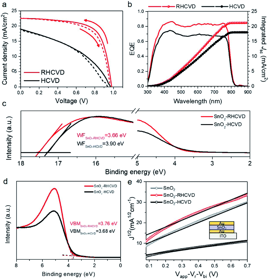 | ||
| Fig. 3 (a) J–V curves of the champion PSCs based on RHCVD and the regular HCVD process with forward and reverse scans. (b) IPCE spectra of the champion PSCs based on RHCVD and the regular HCVD process. (c) UPS spectra of the SnO2 films treated via the RHCVD process and the regular HCVD process. (d) Enlarged UPS valence features of the SnO2 films based on the RHCVD process and the regular HCVD process. (e) Electron mobilities for the as-prepared SnO2 film, and the SnO2 film after the RHCVD process and the regular HCVD process using the SCLC method. The device structure of ITO/Au/SnO2/Au is shown as the inset. | ||
| Scan direction | V OC (V) | J SC (mA cm−2) | FF (%) | PCE (%) | ||
|---|---|---|---|---|---|---|
| RHCVD | Champion | Reverse | 0.99 | 22.3 | 70.2 | 15.5 |
| Forward | 0.97 | 22.6 | 64.5 | 14.1 | ||
| Average | Reverse | 0.98 ± 0.01 | 22.2 + 0.4 | 65.8 ± 3.5 | 14.3 ± 0.8 | |
| Forward | 0.96 ± 0.02 | 22.3 + 0.4 | 63.9 ± 1.9 | 13.9 ± 0.6 | ||
| Regular HCVD | Champion | Reverse | 0.96 | 19.0 | 42.1 | 7.6 |
| Forward | 0.93 | 18.8 | 40.0 | 7.0 | ||
| Average | Reverse | 0.91 ± 0.05 | 17.5 + 1.0 | 43.9 ± 1.4 | 7.0 ± 0.3 | |
| Forward | 0.93 ± 0.04 | 17.5 + 1.2 | 42.4 ± 1.7 | 6.8 ± 0.3 |
We further studied the defect density of the SnO2 films that experienced different vacuum annealing processes to understand their influence on the PSC device performance. Ultraviolet photoemission spectroscopy (UPS) and XPS measurements were carried out to characterize the surface properties of the SnO2 films after the vacuum annealing process. To understand the surface properties, SnO2 films coated on ITO substrates were placed into the CVD tube furnace to simulate the vacuum annealing process during RHCVD and regular HCVD. No organic precursors were loaded into the CVD furnace for the study on the effects of temperature and vacuum conditions. As shown in Fig. 3c, the SnO2 film that experienced the RHCVD vacuum annealing process shows a lower work function (WF) of 3.66 eV, while for the SnO2 film that experienced the regular HCVD vacuum annealing process the WF is much higher (3.90 eV). As for the ETL layer, a lower WF is expected to better facilitate electron extraction.32,33 This explains why the PSC devices based on the SnO2 ETL that experienced long vacuum annealing showed poorer performance. The gap state density between the valence band minimum and the Fermi level also increases for the longer vacuum annealing process (Fig. 3c).15 The enlarged UPS valence features (Fig. 3d) and high resolution XPS valence features (Fig. S10†) further confirm the increased gap states between the valence band and the Fermi level. These gap states lower the hole blocking barrier and increase recombination, hence lowering the VOC and the PCE of the PSCs.27 We used the space-charge limited-current (SCLC) technique to characterize the electronic properties of the devices based on the symmetric sandwich structure (see the inset in Fig. 3e). The mobility was calculated using the Mott–Gurney law.34 The mobility for the freshly coated SnO2 film was 5.0 × 10⁻⁴ cm2 V−1 s−1. After the shorter vacuum annealing process (10 min) to simulate the RHCVD process, the mobility of the SnO2 film became 5.1 × 10⁻⁴ cm2 V−1 s−1, which was almost the same as before. However, the mobility for the SnO2 film that experienced a longer vacuum annealing process of 230 min showed a much lower mobility of 1.7 × 10⁻⁴ cm2 V−1 s−1, which is likely the result of the increased gap states acting as scattering/trapping centers. These observations strongly suggest that RHCVD not only significantly reduces the deposition time, but also maintains the high quality of the SnO2 nanocrystal ETL, which is the main reason for the improvement of PCE up to 15.5%.
To help understand the main reason responsible for the current density reduction, we studied the energy level alignment based on perovskite and SnO2 for the case of RHCVD versus regular HCVD (Fig. S11†). Similar to the previous reports on planar PSCs based on the SnO2 and TiO2 ETL, the energy level mismatch at the perovskite/TiO2 interface prevents efficient charge extraction and therefore leads to reduced current density.35–39 Here in this work, the conduction band of the SnO2 film that experienced the regular HCVD process shows an upward shift, and the work function also increases by 0.24 eV. There is an energy barrier for electron extraction from the perovskite film to SnO2. For the SnO2 film that experienced the RHCVD process, the energy level alignment between the perovskite and SnO2 is better (Fig. S11†). The low work function helps facilitate electron extraction. Furthermore, with a longer vacuum annealing during the regular HCVD process, more gap states are formed above the valence band of the SnO2 film, which lowers the hole blocking properties of this interface and increases charge carrier recombination (Fig. S11†).27
To further verify that vacuum annealing deteriorates charge carrier extraction and increases charge carrier recombination, we fabricated PSCs based on solution-coated perovskite films deposited on a SnO2 ETL with and without vacuum annealing, and the results are shown in Fig. S12.† As we can see, the PSC device based on the SnO2 ETL film after a long time of vacuum annealing shows lower performance with reduced open circuit voltage, short circuit current density and fill factor, which agrees with our previous results.15 On the other hand, the PSC device based on the SnO2 ETL film after a short time of vacuum annealing as in the RHCVD process does not show much difference between the control sample case and the RHCVD-treated SnO2 case. The faster carrier extraction from the perovskite film to the SnO2 ETL after the RHCVD process is further verified by the time resolved photoluminescence (TRPL) spectra (Fig. S13 and Table S2†). The resulting curves are fitted by a double exponential model with fast and slow decay time constants (τ1 and τ2).36 The fast decay time constant τ1 corresponds to the quenching of charge carriers by electron extraction from CH3NH3PbI3 to SnO2.27 With the reduced vacuum annealing process time, the fast time constant τ1 decreased from 17.8 ns for CH3NH3PbI3 on SnO2-HCVD to 10.9 ns for CH3NH3PbI3 on SnO2-RHCVD. This observation also implies that a longer vacuum annealing process may increase the gap states and deteriorate the quality of the SnO2 layer.
In the case of regular HCVD, the combination of mismatched energy levels between the SnO2 ETL and the perovskite film, increased gap states in the SnO2 ETL, and reduced mobility of the SnO2 film contributed to the decreased solar cell performance. The major differences between the regular HCVD and RHCVD are summarized in Table 2.
| J. Mater. Chem. A, 2019, 7, 6920–6929 | This work | |
|---|---|---|
| Deposition time | A total of 230 min (including ramping, deposition, and cooling) | Less than 10 min with a rapid ramping and deposition process |
| The heating component | In the regular HCVD process, the tube furnace is heated by resistive heating (i.e., using filaments); the ramping of the temperature is slow and temperature fluctuation is large | For the RHCVD process, we use a rapid thermal annealing tube furnace, which uses an infrared (IR) heating component with stable control of temperature. The IR heating component is mechanically movable along the furnace tube, which enables fast heating and cooling. This is the first report to apply this rapid thermal annealing process for the fabrication of PSCs and PSMs |
| ETL structure | The SnO2 ETL was deposited by a sputtering process at room temperature and it is amorphous in structure. Due to the prolonged vacuum annealing process, the SnO2 quality has been reduced with increased gap states. A thin layer of C60 has been incorporated to maintain the electron extraction and transport properties. However, this complicated the deposition process with one more vacuum deposition step | In this work, the SnO2 ETL was prepared using a solution of SnO2 nanocrystals |
| Hysteresis and device performance | Due to the prolonged vacuum annealing process and induced gap states in the SnO2 ETL, the solar cells and modules showed hysteresis. And a module with a 22.4 cm2 designated area showed a PCE of 10%, and that with a 91.8 cm2 designated area showed a PCE of 9.34% | In the case of RHCVD, the solar cells and modules showed substantially reduced hysteresis with high-quality SnO2. PSMs with a designated area of 22.4 cm2 showed a PCE of 12.3% |
| Operational stability | The T80 lifetime is around 500 h | The T90 lifetime is over 800 h. The much better operation stability is most likely due to the higher quality of the SnO2 ETL, i.e., the new RHCVD method leads to a lower density of gap states in the SnO2 ETL |
The balance between the temperature ramping time, deposition time and perovskite layer thickness has been studied to further optimize the RHCVD process. Higher temperatures can shorten the deposition time. However, the deposition rate of FAI and the reaction between deposited FAI and PbI2 need to be balanced. If FAI is deposited faster than its reaction with PbI2, there will be excess FAI on top of the perovskite film. When FAI is deposited substantially slower than its reaction with PbI2, the feeding of FAI will be the time limiting factor and a longer time is needed for the complete conversion of PbI2 to perovskite. The optimized condition for RHCVD corresponds to a balanced condition required for vaporization of FAI, diffusion into PbI2 and reaction with PbI2.15,40 Upon temperature increase, both the FAI deposition rate and the reaction rate with PbI2 increase. As the temperature increased to 170 °C (RHCVD-2 in Fig. 4a), the device performance started to decrease (Fig. 4b), which indicates a faster increase of the FAI deposition rate compared with its reaction rate with PbI2, and a pale surface on the top of the perovskite film was observed after being taken out from the tube. On the other hand, with a slower ramping rate (RHCVD-3 in Fig. 4a), the total vacuum annealing time will increase, and the WF of the SnO2 ETL prepared from the SnO2 nanocrystal rises slightly (Fig. 4c). Based on these observation, a shorter reaction time and higher ramping rate benefit the formation of high-quality perovskite films and SnO2 film. The thickness of the PbI2 film also influences the deposition time because a thicker PbI2 film would need more FAI for the conversion to perovskite. To ensure sufficient light absorbance, a film thickness of 370 nm for the perovskite was chosen in this work (Fig. S14†).5
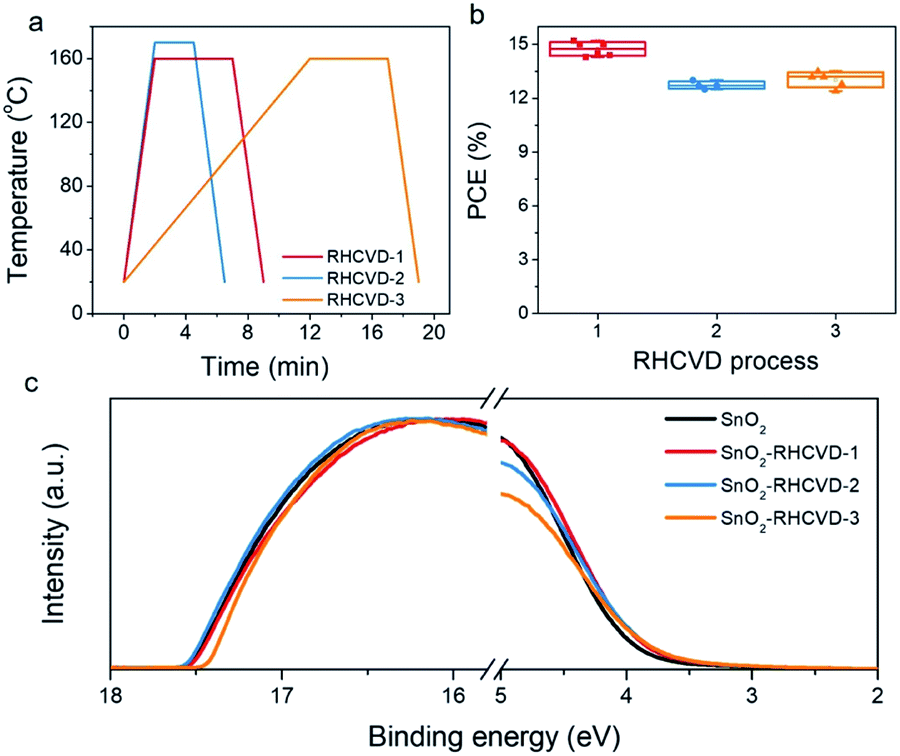 | ||
| Fig. 4 (a) Temperature profiles as a function of time during different RHCVD processes. The RHCVD-2 process has a higher temperature and a shorter treatment time compared with the RHCVD-1 process. The RHCVD-3 process has a slower ramping rate during the temperature increase step compared with the RHCVD-1 process. (b) The dependence of PCE on the different RHCVD processes. (c) UPS spectra of the SnO2 films treated with different RHCVD processes. | ||
HCVD is promising for upscalable fabrication of PSCs. 10 cm × 10 cm PSMs have been demonstrated for the regular HCVD process and the upscaling of the size from 0.1 cm2 to 91.8 cm2 shows a small absolute PCE decay rate of 1.3% per decade of the area increase.15 Similarly, in this work we also tested upscalable capability of RHCVD. Here the CVD tube furnace used for the RHCVD process has an inner diameter of 96 mm, which is the only limitation for the size of the substrates to be used. We fabricated a PSM on a 5 cm × 5 cm substrate using the RHCVD process. The PSM has a designated area of 22.4 cm2 with 7 cells connected in series. For each subcell the ITO stripe width is 6.6 mm, and there is a 0.1 mm P1 patterning line between each sub stripe. The length of each sub-cell is 4.8 cm, with 1 mm space at the edges that are perpendicular to the patterning lines. The edges that are parallel to the patterning line have a space of 1.5 mm and are used for wiring of the electrodes (Fig. S15†). The typical geometric fill factor for the module is approximately 90%.15,27 The champion PSM has a PCE of 12.3% and almost no hysteresis (Fig. 5a and b). Furthermore, the continuous operation of the PSM under continuous light illumination in a dry N2 box was measured by recording the PSM power output under a steady voltage output, which corresponded to the initial maximum power point voltage. As shown in Fig. 5c, the power output of the PSM maintained 90% of its initial value after continuous working under light illumination after 800 h. The RHCVD process shows a significantly shorter processing time and longer operation stability and is a promising method for upscalable fabrication of PSMs with larger areas, smaller PCE decay and longer operational lifetime (Table S3†).
 | ||
| Fig. 5 PSMs fabricated via the RHCVD process. (a) A photograph of a 5 cm × 5 cm PSM. (b) A forward scan and reverse scan from the PSM with the best performance of 12.3%. (c) The continuous operation of PSMs under continuous light illumination. | ||
Experimental
Materials
All the commercial materials were used as received without further purification, including SnO2 (Alfa Aesar, tin(IV) oxide, 15% in H2O colloidal dispersion), PbI2 (99.99%, TCI), CsI (99.99% Sigma), formamidinium iodide (FAI, greatcell solar), isopropanol (Wako), and 2,2′,7,7′-tetrakis(N,N-di-p-methoxyphenylamine)-9,9′-spirobifluorene (spiro-MeOTAD, Merck).Solar cell device fabrication
Indium-doped tin oxide (ITO) substrates were washed with distilled water, acetone and isopropanol in sequence, and dried with N2 gas. Before the usage of the ITO substrates, they were pre-treated under UV/O3 for 30 min. The SnO2 layer was coated on the ITO surface by spin coating of the SnO2 nanocrystal solution (2.5% in distilled water) at 3000 rpm for 30 s, followed by drying at 150 °C for 30 min. The perovskite precursor layer was deposited by a thermal co-evaporation process of PbI2 and CsI, which was reported in our previous work.15 Here the evaporation rate of PbI2 and CsI was controlled to be 0.10 nm s−1 and 0.01 nm s−1, respectively. Then the PbI2/CsI-coated substrate was transferred to a single-zone tube or a multi-zone tube furnace to conduct the RHCVD process or the regular HCVD process. After reaction and cooling, the resultant perovskite film was washed with IPA solution, followed by heating at 100 °C for 20 min to remove the residual FAI on the surface of the perovskite. A hole transport material solution was spin-coated on top of the perovskite layer at the rotation speed of 3000 rpm for 30 s. The hole transport material solution contained 29 mg of spiro-MeOTAD, 11.5 μL of TBP and 7 μL of Li-TFSI solution in 0.4 mL chlorobenzene. Finally, a layer of 100 nm thickness of gold was evaporated as the back-contact electrode. For module fabrication, the Au electrode thickness was 120 nm.RHCVD
Detailed steps of the RHCVD process for the deposition of perovskite films are depicted in Fig. 1. In brief, the RHCVD process is performed in a single-zone tube furnace with FAI powder as the precursor. At one end of the tube furnace a vacuum pump is connected, and at the other end a vacuum gauge is connected and controls the vacuum level of the furnace to 10 Torr. During the RHCVD process, a sufficient amount of FAI powder (0.1 g) is placed in the upstream zone of the furnace close to the pre-deposited CsI/PbI2 substrate. After the reaction, the furnace is moved and the heating zone is cooled with a fan to accelerate the cooling speed of the tube.Characterization
Surface morphology was observed using an SEM (FEI Quanta 250 FEG). The UPS and XPS spectra were recorded using an XPS-AXIS Ultra HAS (Kratos) with monochromatic Al-Kα = 1486.6 eV and non-monochromatic He-Iα = 21.22 eV sources. The crystal structure of the perovskite was analysed using XRD (Bruker D8 Discover). J–V curves of the solar cells were measured using a Keithley 2420 Source Meter under AM1.5 illumination generated from a solar simulator (Oriel-Sol3A). The illumination intensity of 100 mW cm−2 was adjusted by using a reference silicon solar cell before the measurements of the PSCs and PSMs.Conclusions
In this work, we report a RHCVD method, which can help maintain a high-quality SnO2 ETL and enable the deposition of high-quality perovskite layers. The significant reduction in the processing time from several hours to less than 10 minutes can substantially increase the perovskite solar cell production throughput. After optimization of the various parameters for the RHCVD fabrication (e.g., process temperature, perovskite layer thickness, SnO2 ETL, etc.), we obtained PSCs with PCEs up to 15.5% and PSMs with a PCE of 12.3%. The fabrication of PSMs shows the upscalable capabilities of this RHCVD method. Furthermore, the fabricated PSM shows a high operational stability and maintains 90% of its initial PCE value after 800 hours of continuous operation under light illumination.Conflicts of interest
Yabing Qi, Longbin Qiu, Sisi He, and Luis K. Ono are named inventors on the patent application 63036068 (filing date: June 8, 2020), which is related to the techniques described in this article.Acknowledgements
This work was supported by funding from the Energy Materials and Surface Sciences Unit of the Okinawa Institute of Science and Technology Graduate University, the OIST Proof of Concept (POC) Program, and the OIST R&D Cluster Research Program. We thank the OIST Mech. Eng. & Microfabrication Support Section for maintenance of the cleanroom and the OIST Imaging Section for support.References
- M. A. Green, E. D. Dunlop, J. Hohl-Ebinger, M. Yoshita, N. Kopidakis and X. Hao, Solar cell efficiency tables (Version 55), Prog. Photovolt: Res. Appl., 2020, 28, 629–638 CrossRef.
- M. Cai, Y. Wu, H. Chen, X. Yang, Y. Qiang and L. Han, Cost-Performance Analysis of Perovskite Solar Modules, Adv. Sci., 2017, 4, 1600269 CrossRef.
- S. He, L. Qiu, L. K. Ono and Y. B. Qi, How far are we from attaining 10-year lifetime for metal halide perovskite solar cells?, Mater. Sci. Eng., R, 2020, 140, 100545 CrossRef.
- S. Chu, Y. Cui and N. Liu, The path towards sustainable energy, Nat. Mater., 2017, 16, 16–22 CrossRef.
- L. Qiu, S. He, L. K. Ono, S. Liu and Y. B. Qi, Scalable Fabrication of Metal Halide Perovskite Solar Cells and Modules, ACS Energy Lett., 2019, 4, 2147–2167 CrossRef CAS.
- Z. Li, T. R. Klein, D. H. Kim, M. Yang, J. J. Berry, M. F. A. M. van Hest and K. Zhu, Scalable fabrication of perovskite solar cells, Nat. Rev. Mater., 2018, 3, 18017 CrossRef CAS.
- N.-G. Park and K. Zhu, Scalable fabrication and coating methods for perovskite solar cells and solar modules, Nat. Rev. Mater., 2020, 5, 333–350 CrossRef CAS.
- X. Dai, Y. Deng, C. H. Van Brackle, S. Chen, P. N. Rudd, X. Xiao, Y. Lin, B. Chen and J. Huang, Scalable Fabrication of Efficient Perovskite Solar Modules on Flexible Glass Substrates, Adv. Energy Mater., 2020, 10, 1903108 CrossRef CAS.
- M. Yang, D. H. Kim, T. R. Klein, Z. Li, M. O. Reese, B. J. Tremolet de Villers, J. J. Berry, M. F. A. M. van Hest and K. Zhu, Highly Efficient Perovskite Solar Modules by Scalable Fabrication and Interconnection Optimization, ACS Energy Lett., 2018, 3, 322–328 CrossRef CAS.
- R. Patidar, D. Burkitt, K. Hooper, D. Richards and T. Watson, Slot-die coating of perovskite solar cells: an overview, Mater. Today Commun., 2020, 22, 100808 CrossRef CAS.
- M. Remeika, S. R. Raga, S. Zhang and Y. B. Qi, Transferrable optimization of spray-coated PbI2 films for perovskite solar cell fabrication, J. Mater. Chem. A, 2017, 5, 5709–5718 RSC.
- L. Gil-Escrig, C. Momblona, M.-G. La-Placa, P. P. Boix, M. Sessolo and H. J. Bolink, Vacuum Deposited Triple-Cation Mixed-Halide Perovskite Solar Cells, Adv. Energy Mater., 2018, 8, 1703506 CrossRef.
- Y. Jiang, M. Remeika, Z. Hu, E. J. Juarez-Perez, L. Qiu, Z. Liu, T. Kim, L. K. Ono, D.-Y. Son, Z. Hawash, M. R. Leyden, Z. Wu, L. Meng, J. Hu and Y. B. Qi, Negligible-Pb-Waste and Upscalable Perovskite Deposition Technology for High-Operational-Stability Perovskite Solar Modules, Adv. Energy Mater., 2019, 9, 1803047 CrossRef.
- M. R. Leyden, L. K. Ono, S. R. Raga, Y. Kato, S. Wang and Y. B. Qi, High performance perovskite solar cells by hybrid chemical vapor deposition, J. Mater. Chem. A, 2014, 2, 18742–18745 RSC.
- L. Qiu, S. He, Y. Jiang, D.-Y. Son, L. K. Ono, Z. Liu, T. Kim, T. Bouloumis, S. Kazaoui and Y. B. Qi, Hybrid chemical vapor deposition enables scalable and stable Cs-FA mixed cation perovskite solar modules with a designated area of 91.8 cm2 approaching 10% efficiency, J. Mater. Chem. A, 2019, 7, 6920–6929 RSC.
- J. Yin, H. Qu, J. Cao, H. Tai, J. Li and N. Zheng, Vapor-assisted crystallization control toward high performance perovskite photovoltaics with over 18% efficiency in the ambient atmosphere, J. Mater. Chem. A, 2016, 4, 13203–13210 RSC.
- M. M. Tavakoli, S. M. Zakeeruddin, M. Grätzel and Z. Fan, Large-Grain Tin-Rich Perovskite Films for Efficient Solar Cells via Metal Alloying Technique, Adv. Mater., 2018, 30, 1705998 CrossRef.
- M. M. Tavakoli, L. Gu, Y. Gao, C. Reckmeier, J. He, A. L. Rogach, Y. Yao and Z. Fan, Fabrication of efficient planar perovskite solar cells using a one-step chemical vapor deposition method, Sci. Rep., 2015, 5, 14083 CrossRef.
- M.-H. Li, H.-H. Yeh, Y.-H. Chiang, U.-S. Jeng, C.-J. Su, H.-W. Shiu, Y.-J. Hsu, N. Kosugi, T. Ohigashi, Y.-A. Chen, P.-S. Shen, P. Chen and T.-F. Guo, Highly Efficient 2D/3D Hybrid Perovskite Solar Cells via Low-Pressure Vapor-Assisted Solution Process, Adv. Mater., 2018, 30, 1801401 CrossRef.
- L. Luo, Y. Zhang, N. Chai, X. Deng, J. Zhong, F. Huang, Y. Peng, Z. Ku and Y.-B. Cheng, Large-area perovskite solar cells with CsxFA1−xPbI3−yBry thin films deposited by a vapor–solid reaction method, J. Mater. Chem. A, 2018, 6, 21143–21148 RSC.
- J. H. Kim, P.-W. Liang, S. T. Williams, N. Cho, C.-C. Chueh, M. S. Glaz, D. S. Ginger and A. K.-Y. Jen, High-Performance and Environmentally Stable Planar Heterojunction Perovskite Solar Cells Based on a Solution-Processed Copper-Doped Nickel Oxide Hole-Transporting Layer, Adv. Mater., 2015, 27, 695–701 CrossRef CAS.
- S.-H. Turren-Cruz, A. Hagfeldt and M. Saliba, Methylammonium-free, high-performance, and stable perovskite solar cells on a planar architecture, Science, 2018, 362, 449–453 CrossRef CAS.
- Y. Jiang, M. R. Leyden, L. Qiu, S. Wang, L. K. Ono, Z. Wu, E. J. Juarez-Perez and Y. B. Qi, Combination of Hybrid CVD and Cation Exchange for Upscaling Cs-Substituted Mixed Cation Perovskite Solar Cells with High Efficiency and Stability, Adv. Funct. Mater., 2018, 28, 1703835 CrossRef.
- W. Xiong, Y. S. Zhou, L. J. Jiang, A. Sarkar, M. Mahjouri-Samani, Z. Q. Xie, Y. Gao, N. J. Ianno, L. Jiang and Y. F. Lu, Single-Step Formation of Graphene on Dielectric Surfaces, Adv. Mater., 2013, 25, 630–634 CrossRef CAS.
- E. J. Juarez-Perez, Z. Hawash, S. R. Raga, L. K. Ono and Y. B. Qi, Thermal degradation of CH3NH3PbI3 perovskite into NH3 and CH3I gases observed by coupled thermogravimetry-mass spectrometry analysis, Energy Environ. Sci., 2016, 9, 3406–3410 RSC.
- E. J. Juarez-Perez, L. K. Ono, M. Maeda, Y. Jiang, Z. Hawash and Y. B. Qi, Photodecomposition and thermal decomposition in methylammonium halide lead perovskites and inferred design principles to increase photovoltaic device stability, J. Mater. Chem. A, 2018, 6, 9604–9612 RSC.
- L. Qiu, Z. Liu, L. K. Ono, Y. Jiang, D.-Y. Son, Z. Hawash, S. He and Y. B. Qi, Scalable Fabrication of Stable High Efficiency Perovskite Solar Cells and Modules Utilizing Room Temperature Sputtered SnO2 Electron Transport Layer, Adv. Funct. Mater., 2019, 29, 1806779 CrossRef CAS.
- K.-H. Jung, J.-Y. Seo, S. Lee, H. Shin and N.-G. Park, Solution-processed SnO2 thin film for a hysteresis-free planar perovskite solar cell with a power conversion efficiency of 19.2%, J. Mater. Chem. A, 2017, 5, 24790–24803 RSC.
- Q. Jiang, L. Zhang, H. Wang, X. Yang, J. Meng, H. Liu, Z. Yin, J. Wu, X. Zhang and J. You, Enhanced electron extraction using SnO2 for high-efficiency planar-structure HC(NH2)2PbI3-based perovskite solar cells, Nat. Energy, 2016, 2, 16177 CrossRef.
- Q. Jiang, X. Zhang and J. You, SnO2: A Wonderful Electron Transport Layer for Perovskite Solar Cells, Small, 2018, 14, 1801154 CrossRef.
- M. Saliba and L. Etgar, Current Density Mismatch in Perovskite Solar Cells, ACS Energy Lett., 2020, 5, 2886–2888 CrossRef CAS.
- Y. Zhou, C. Fuentes-Hernandez, J. Shim, J. Meyer, A. J. Giordano, H. Li, P. Winget, T. Papadopoulos, H. Cheun, J. Kim, M. Fenoll, A. Dindar, W. Haske, E. Najafabadi, T. M. Khan, H. Sojoudi, S. Barlow, S. Graham, J.-L. Brédas, S. R. Marder, A. Kahn and B. Kippelen, A Universal Method to Produce Low-Work Function Electrodes for Organic Electronics, Science, 2012, 336, 327–332 CrossRef CAS.
- L. Qiu, L. K. Ono, Y. Jiang, M. R. Leyden, S. R. Raga, S. Wang and Y. B. Qi, Engineering Interface Structure to Improve Efficiency and Stability of Organometal Halide Perovskite Solar Cells, J. Phys. Chem. B, 2018, 122, 511–520 CrossRef CAS.
- D. Yang, R. Yang, K. Wang, C. Wu, X. Zhu, J. Feng, X. Ren, G. Fang, S. Priya and S. Liu, High efficiency planar-type perovskite solar cells with negligible hysteresis using EDTA-complexed SnO2, Nat. Commun., 2018, 9, 3239 CrossRef.
- J. P. Correa Baena, L. Steier, W. Tress, M. Saliba, S. Neutzner, T. Matsui, F. Giordano, T. J. Jacobsson, A. R. Srimath Kandada, S. M. Zakeeruddin, A. Petrozza, A. Abate, M. K. Nazeeruddin, M. Grätzel and A. Hagfeldt, Highly efficient planar perovskite solar cells through band alignment engineering, Energy Environ. Sci., 2015, 8, 2928–2934 RSC.
- H. Yu, H.-I. Yeom, J. W. Lee, K. Lee, D. Hwang, J. Yun, J. Ryu, J. Lee, S. Bae, S. K. Kim and J. Jang, Superfast Room-Temperature Activation of SnO2 Thin Films via Atmospheric Plasma Oxidation and their Application in Planar Perovskite Photovoltaics, Adv. Mater., 2018, 30, 1704825 CrossRef.
- D. Yang, X. Zhou, R. Yang, Z. Yang, W. Yu, X. Wang, C. Li, S. Liu and R. P. H. Chang, Surface optimization to eliminate hysteresis for record efficiency planar perovskite solar cells, Energy Environ. Sci., 2016, 9, 3071–3078 RSC.
- D. Yang, R. Yang, K. Wang, C. Wu, X. Zhu, J. Feng, X. Ren, G. Fang, S. Priya and S. F. Liu, High efficiency planar-type perovskite solar cells with negligible hysteresis using EDTA-complexed SnO2, Nat. Commun., 2018, 9, 3239 CrossRef.
- Z. Liu, L. Qiu, L. K. Ono, S. He, Z. Hu, M. Jiang, G. Tong, Z. Wu, Y. Jiang, D.-Y. Son, Y. Dang, S. Kazaoui and Y. B. Qi, A holistic approach to interface stabilization for efficient perovskite solar modules with over 2000-hour operational stability, Nat. Energy, 2020, 5, 596–604 CrossRef CAS.
- M. R. Leyden, M. V. Lee, S. R. Raga and Y. B. Qi, Large formamidinium lead trihalide perovskite solar cells using chemical vapor deposition with high reproducibility and tunable chlorine concentrations, J. Mater. Chem. A, 2015, 3, 16097–16103 RSC.
Footnotes |
| † Electronic supplementary information (ESI) available. See DOI: 10.1039/d0ta09007g |
| ‡ L. Qiu and S. He contributed equally to this work. |
| This journal is © The Royal Society of Chemistry 2020 |