DOI:
10.1039/D0TA08839K
(Paper)
J. Mater. Chem. A, 2020,
8, 25245-25254
Prediction of higher thermoelectric performance in BiCuSeO by weakening electron–polar optical phonon scattering†
Received
8th September 2020
, Accepted 12th November 2020
First published on 19th November 2020
Abstract
BiCuSeO is a promising thermoelectric material, but its applications are hindered by low carrier mobility. We use first-principles calculations to analyse electron–phonon scattering mechanisms and evaluate their contributions to the thermoelectric figure of merit ZT. The combined scattering of carriers by polar optical (PO) and longitudinal acoustic (LA) phonons yields an intrinsic hole mobility of 32 cm2 V−1 s−1 at room temperature and a temperature power law of T−1.5 between 100–875 K, which agree well with experiments. We demonstrate that electron–phonon scattering in the Cu–Se layer dominates at low T (< 500 K), while contributions from the Bi–O layer become increasingly significant at higher T. At room temperature, ZT is calculated to be 0.48 and can be improved by 30% through weakening PO phonon scattering in the Cu–Se layer. This finding agrees with the experimental observation that weakening the electron–phonon interaction by Te substitution in the Cu–Se layer improves mobility and ZT. At high T, the figure of merit is improved by weakening the electron–PO phonon scattering in the Bi–O layer instead. The theoretical ZT limit of BiCuSeO is calculated to be 2.5 at 875 K.
Introduction
Thermoelectric materials are attracting increasing attention in applications such as waste heat recovery and solid-state cooling.1–3 The thermoelectric performance of materials is evaluated by the dimensionless thermoelectric figure of merit ZT, which is determined by the interplay of Seebeck coefficient S, electrical conductivity σ, thermal conductivity κ, and absolute temperature T through the equation ZT = S2σT/κ. The combined quantity S2σ is called thermoelectric power factor, and κ is composed of electrical thermal conductivity κe and lattice thermal conductivity κL, i.e. κ = κe + κL. Oxides were once believed to be poor thermoelectric materials due to their high thermal conductivity and low carrier mobility.3 However, practical high temperature thermoelectric applications call for oxides because of their high thermal and chemical stability. Currently, several families of promising thermoelectric oxides have been discovered,3–5 among which NaxCoO2 and SrTiO3 based materials possess relatively high thermoelectric power factor.6,7 Mixed anion compounds, such as the layered BiCuSeO which combines characteristics of both oxide and chalcogenide materials, are advantageous in thermoelectric applications because of their intrinsically low thermal conductivity (∼1 W m−1 K−1 at room temperature) and high thermal stability.8,9 BiCuSeO-based materials have emerged as state-of-the-art thermoelectric oxychalcogenides since 2010.8–10 Various doping strategies, such as substitution of Bi with alkali,11,12 alkaline earth,9,13–16 and post-transition metals such as lead,17–20 have been successfully demonstrated to obtain ZT values close to or beyond unity at high temperatures. The highest p-type ZT has reached 1.5 at 873 K by employing a dual-doping method at the Bi site in Bi0.88Ca0.06Pb0.06OCuSe.21 However, the low carrier mobility of BiCuSeO (∼20 cm2 V−1 s−1vs. 525 cm2 V−1 s−1 of Bi2Te3 at room temperature) limits further optimisation of its thermoelectric performance.1,20,22
Up to now, much theoretical efforts have been devoted to investigating the phonon transport properties of BiCuSeO in order to unravel the reason behind the ultralow thermal conductivity, which has been attributed to high Grüneisen parameter,23 acoustic–optical phonon hybridization at low frequency range,24 low frequency vibrations arising from weak bonding of Cu atoms,25 and also a remarkable contribution from high frequency optical phonons due to O vibrations.26 On the other hand, computational analysis that applies deformation potential (DP) theory has been used to explain the charge transport properties of BiCuSeO by assuming that scattering from the longitudinal acoustic (LA) phonon dominates charge transport,27–29 which is based on the fact that the measured mobility obeys the temperature power law of T−1.5.15,30 This power law is normally observed when the band edges can be represented by the single parabolic band (SPB) approximation.22,28,31 However, there is an eight-fold valley degeneracy near the valence band maxima of BiCuSeO as revealed in previous work,27 so the assumption of SPB in BiCuSeO is debatable. In addition, past computational studies have neglected electron–polar optical (PO) phonon scattering. This mechanism, accounting for the interaction between charge carriers and the electric field generated by vibrations of atoms with opposite charge, is important for semiconductors such as SrTiO3 and CH3NH3PbI3,32–34 because of the large electronegativity difference between different elements. Recent experimental research hints at the importance of electron–optical phonon scattering in determining the charge transport properties of BiCuSeO.22,35 For example, Te-doping is found to increase the bond covalency in the Cu–Se layer and thus might improve the carrier mobility of BiCuSeO through affecting electron–PO phonon scattering.22 A large temperature dependence of carrier mobility (μ ∼ T−2.28) is found in BiCuSeO single crystals between 50–300 K, which might be due to electron–optical phonon scattering.35 Therefore, electron–PO phonon coupling may be expected to play an important role in BiCuSeO. However, its effect on charge transport and thermoelectric properties of BiCuSeO has not yet been investigated explicitly. Here, by performing first-principles calculations we demonstrate that electron–PO phonon scattering plays a more fundamental role than electron–LA phonon scattering in the charge transport properties of BiCuSeO, particularly at temperatures below 500 K. This is due to a combination of multiple valley effects in the electronic band structure and low-lying optical phonons in the phonon band structure. Our results further highlight that contributions from Cu–Se and Bi–O layers dominate in different temperature ranges and carrier concentrations, and thus suggest ways for rational optimisation of the thermoelectric performance of BiCuSeO.
Computational details
Accurate calculation of the crystal structure of BiCuSeO requires careful account of dispersion contributions in the interlayer interaction. The electronic structure necessitates a proper description of the strongly correlated d orbitals on Cu, and the relativistic effects for the heavy Bi ions. In addition, charge transport calculations need very fine sampling of the band structure in reciprocal space, and the phonon dispersion requires calculation through supercell expansions or perturbation theory. The combinations of all the above features make calculating the thermoelectric figure of merit of BiCuSeO a formidable computational task. To make the solution feasible, without loss of accuracy, we have employed different formulations of density functional theory (DFT) for individual components of the analysis. An in-depth analysis of how the choice of DFT functional affects structural and electronic properties of BiCuSeO is provided in the ESI (Tables S1–S4 and Fig. S1–S6).†
All calculations employed the Vienna ab initio simulation package (VASP).36,37 All structural observables, including geometry optimisations, elastic constants, and phonon dispersion have been calculated using the optB86b-vdW functional38 that accounts for the van der Waals interactions between layers. The cut-off energy of the plane wave basis set was 550 eV. The k-mesh in optimisation was 11 × 11 × 5. The energy and force convergence criteria were 1 × 10⁻⁵ eV and 1 × 10⁻² eV Å−1, respectively. The optimised lattice parameters compare well with experiment (Table S1†). The calculated Brillouin zone centre phonon frequencies for the polar optical phonon modes are in very close agreement to experiment and previous calculation (see Table S2†). Phonon band structure and phonon density of states (DOS) were obtained by combining VASP with phonopy39 using a 4 × 4 × 4 supercell (512 atoms). The longitudinal optical and transverse optical (LO–TO) splitting was included. Born effective charges are shown in Table S3.† Our analysis in ESI indicates the inclusion of spin–orbit coupling (SOC) and orbital dependent parameters are vital for obtaining accurate electronic band structure. In addition, the comparison of band structure calculated by using optB86b-vdW and PBE (Fig. S2 and S3, ESI†) show that the exclusion of van der Waals interaction and the transit of exchange functional from optB86b to PBE have negligible effect on electronic states at band edges. Furthermore, Table S1† shows that inclusion of SOC and orbital dependent parameters has a minimal effect on the lattice parameters, comparing a and c optimised by using PBE, PBE+U, PBE+SOC and PBE+U+SOC functionals. The PBE+U+SOC functional alone, however, overestimates the lattice parameters (Table S1†), underestimates PO phonon frequency and elastic constants (Tables S2 and S4†), as the van der Waals interaction is vital for structural properties. Therefore, for feasibility and avoiding loss of accuracy, all electronic properties, including the electronic band structure and all observables derived from analysis of the band structure, have been calculated using the PBE+U+SOC functional, based upon the optB86b-vdW optimised crystal structure. Spin–orbit coupling (SOC) was treated self-consistently via perturbational methods. Two-component treatment was used through non-collinear magnetic structure calculation. The SOC operator was expressed using the zeroth-order-regular approximation (ZORA).40 A Hubbard U value of 4 eV was added to the Cu 3d orbitals, as validated for Cu-based multinary semiconductors.41 The same setting has also been adopted in earlier band structure calculations of BiCuSeO in literature.42,43 Band structures calculated with PBE+U+SOC and the hybrid exchange HSE06+SOC functionals are compared in Fig. S6.† They show very similar dispersion in reciprocal space; for instance, the effective mass of hole at the valence band maximum along the Γ–M direction is 0.21m0 in both setups. Further comparisons are discussed in the Results section. Uncorrelated PBE+SOC calculations yield instead a metallic solution with zero band gap (Fig. S3†). A rigid shift of 0.44 eV of the conduction band levels (scissor operator) to reproduce the experimental band gap of 0.8 eV (ref. 44) has been applied to the PBE+U+SOC results for calculations of the transport properties.
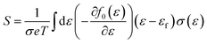
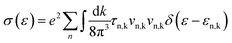
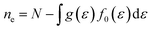
Boltzmann transport theory in relaxation time approximation as implemented in the BoltzTraP code45 was employed to calculate the charge carrier mobility and thermoelectric coefficients of BiCuSeO. The electrical conductivity σ, Seebeck coefficient S, electrical thermal conductivity κe, carrier concentration ne, and charge carrier mobility μ are calculated as
| |  | (1) |
| |  | (2) |
| |  | (3) |
| |  | (4) |
| |  | (5) |
where
εn,k is the electron energy,
vn,k is the group velocity,
τn,k is the relaxation time,
e is the elementary charge,
T is the absolute temperature,
f0 is the Fermi–Dirac distribution function,
εf is the Fermi energy,
n is the notation of bands,
g is the electron density of states, and
N is the number of electrons within a unit cell. A fine
k-mesh of 31 × 31 × 11 was adopted to calculate electron energy, which was further interpolated 15 times in BoltzTraP in order to converge the calculation of the above charge transport coefficients.
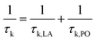
We implemented relaxation time calculation in BoltzTraP to investigate the LA and PO phonon scattering mechanisms. The total relaxation time is calculated according to Matthiessen's rule by:
| |  | (7) |
Deformation potential theory is used to calculate the LA phonon scattering limited relaxation time by:31
| |  | (8) |
where ℏ is the reduced Planck constant,
θ is the scattering angle between
k and
k′, |
M(
k,
k′)| is the scattering matrix calculated as
| |  | (9) |
where
E1,i is the deformation potential constant in three normal directions,
Cii is the corresponding elastic constant,
kB is the Boltzmann constant. The elastic constant
Cii was calculated by using the DFPT formalism in VASP. The deformation potential constant
E1,i was calculated by firstly applying a small strain on the unit cell and then performing a linear fitting of the variation of the energy of valence band maximum (VBM) with strain in three normal directions. The deformation potential constants were calibrated by the Cu 3p core level energy at the
Γ point. Since relaxation time is a scalar quantity, and charge carriers are scattered by acoustic phonons in all directions simultaneously between two scattering events in real materials, the scattering matrix is averaged over three normal directions.
The relaxation time due to PO phonon scattering is calculated by:34,46
| |  | (10) |
when
E > ℏ
ωPO, and
| |  | (11) |
when
E < ℏ
ωPO, where is
E the electron energy,
m* is the effective mass,
ε0 is the vacuum permittivity,
k0 is the static and
k∞ the high-frequency dielectric constant,
ωPO is the frequency of the PO phonon modes,
nq is the Bose–Einstein distribution function of phonons.
E is calculated with respect to VBM for holes. The parameter
m* is obtained by fitting a parabola near the band edges. Since usually
k0 ≫
k∞, 1/
k0 is omitted.
k∞ of BiCuSeO is calculated to be 17.61 and 13.25 for in-plane and out-of-plane directions, respectively, which agree well with previous calculations (18.01 and 13.79 in
ref. 24; 15.3 and 12.0 in
ref. 43). The relaxation time due to multiple PO phonon modes was also added by using the Matthiessen's rule.
While more accurate first principles techniques exist to calculate electron–phonon couplings (EPC), such as density functional perturbation theory (DFPT) and Wannier interpolation,47 these are not yet available in conjunction with orbital dependent functionals (DFT+U or HSE06) that are required to reproduce electronic and phonon band structures of BiCuSeO. Our choice that focuses on the two most important and physically different electron–phonon scattering mechanisms in BiCuSeO is therefore a pragmatic solution to further our understanding of this and related mixed-anion thermoelectrics.
Results and discussion
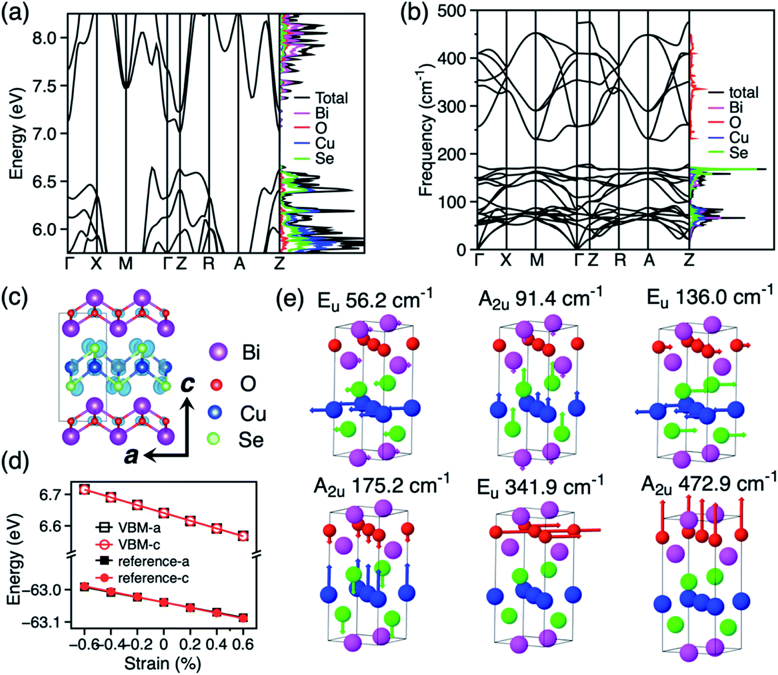
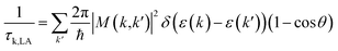
BiCuSeO is formed by ionic layers of composition [Bi2O2]2+ and [Cu2Se2]2−, and adopts a tetragonal cell with space group P4/nmm (Fig. 1c). The optimised lattice constants in our calculation (a = 3.926 Å, c = 8.957 Å) show excellent agreement with experimental values (a = 3.930 Å, c = 8.927 Å).9 As the electronic and phonon band structure are well documented in literature,24,26,27,42 we present our results for band and phonon band structure in the following and compare the key features that determine the charge transport properties of BiCuSeO. The electronic band structures and density of states (DOS) calculated with the PBE+U+SOC functional are shown in Fig. 1a. The calculated band gap is 0.36 eV. The HSE06+SOC calculation shows a band gap of 0.93 eV (Fig. S5†), which is closer to the experimental measure of 0.8 eV.44 The PBE+U+SOC band structure compares well with the more expensive HSE06+SOC result after a rigid band shift (Fig. S6†). The top of the valence band of BiCuSeO is composed of Se and Cu orbitals and the bottom of the conduction band is constituted of Bi orbitals. The valence band maximum (VBM) is located along the Γ–M direction. The charge density at the VBM is shown in Fig. 1c. There are three valence band maxima, one along Γ–M, one at Z and one along Z–R with only a minor energy difference (15 meV between the valence band maxima along Γ–M and at Z, 51 meV between valence band maxima along Γ–M and Z–R). The hole effective mass around the three valence band maxima is calculated to be 0.21m0, 0.68m0, and 4.60m0, (where m0 is the electron mass), respectively, which agree with previous theoretical results (Γ–M: 0.21m0, Z–Γ: 0.47m0, and R–Z: 4.53m0) obtained at the HSE06+SOC level of DFT calculation.27 This warrants the reliability of our chosen PBE+U+SOC setup for further calculation of thermoelectric coefficients of BiCuSeO, as a scissor operator can be applied to reproduce the accurate band dispersion and band gap. The phonon band structure and phonon DOS of BiCuSeO are shown in Fig. 1b. The phonons with frequencies above 200 cm−1 are mainly projected to oxygen and those below 200 cm−1 are mostly due to the heavier atoms. The Γ point has D4h point group symmetry, with phonons belonging to the following irreducible representations: Γ = 4A2u + 2A1g + 2B1g + 4Eu + 4Eg. For the doubly degenerate Eu and Eg modes, atoms vibrate in plane, while for A2u, A1g, and B1g modes, atoms vibrate out of plane. Fig. 1e shows the six PO modes of BiCuSeO. The calculated frequencies of the PO modes compare well with experiment and previous calculation (Table S2†).24 The lower four PO phonon modes with frequencies below 200 cm−1 are mainly due to atomic displacements in the Cu–Se layer, while the two PO modes with frequencies above 200 cm−1 are due to oxygen vibrations in the Bi–O layer.
 |
| | Fig. 1 (a) Electronic band structure and density of states (DOS) of BiCuSeO. (b) Phonon band structure and phonon DOS. (c) Crystal structure of BiCuSeO, and charge distribution for the eigenstate at the VBM. (d) Variation of VBM energy with strain in a and c directions. The reference energy of the Cu-3p core level used to obtain the deformation constants is also shown. (e) Symmetry, frequency and atomic displacements for the PO phonon modes at Γ. | |
In order to discriminate the relative importance of LA and PO phonon scattering on charge transport in BiCuSeO, the electron–LA phonon scattering is calculated by using deformation potential (DP) theory30,31 and the electron–PO phonon scattering is calculated by accounting for the Fröhlich interaction.33 The DP constants are calculated by monitoring the variation of the energy of VBM with strain (Fig. 1d). Although this method is approximate,48 it has previously been successfully applied to describe the electron–LA phonon scattering in CH3NH3PbI3, and the calculated DP constants (4.3 eV for electrons and 1.5 eV for holes)49 are comparable to experimental results (2.93 eV for electrons and 2.2 eV for holes).50 The DP constants for holes in BiCuSeO are calculated to be 4.5 and 4.1 eV in the a and c directions, respectively (Table 1) with PBE+U+SOC functional. We also compared the DP constants calculated with PBE+U (4.8 eV in a and 4.0 eV in c direction, Fig. S7†), which indicates the SOC has a minor effect on DP constants. A deformation potential constant of 24 eV is available in the literature, fitted from experimental data by assuming that LA phonon scattering dominates the charge transport properties of BiCuSeO and the valence band can be represented by a simple parabolic band (SPB) structure.27,28 However, these assumptions are questionable given the multiple maxima present in the band structure,27 such that the deformation potential as high as 24 eV should be taken with caution. We calculated DP constants from first-principles in order to evaluate the relative importance of LA and PO scattering. The elastic constants of BiCuSeO are calculated to be 155.1 and 103.7 GPa in a and c directions, respectively. The calculated Young's modulus is 104.1 and 63.5 GPa in the a and c directions, respectively. The isotropic Young's modulus for polycrystalline samples is calculated to be 98.4 GPa by using the Voigt–Reuss–Hill scheme,51 which agrees well with previous theoretical calculations (93 GPa in ref. 24; 109.3 GPa in ref. 52), but has an overestimation over the experimental value of 76.5 GPa measured on polycrystalline samples.23 The reason of the overestimation might be that theoretical values correspond to 0 K, while experimental measurement is performed at room temperature.
Table 1 Deformation potential constant E1, elastic constant Cii, Young's modulus E, LA phonon scattering limited mobility μLA and average relaxation time τLA, PO phonon scattering limited mobility μPO, and average relaxation time τPO, and the total carrier mobility limited by LA and PO phonon scattering μTotal for holes in BiCuSeO at 300 K
| Direction |
This work |
Experiment |
|
a
|
c
|
|
E
1 (eV) |
4.5 |
4.1 |
|
|
C
ii
(GPa) |
155.1 |
103.7 |
|
|
E (GPa) |
104.1 |
63.5 |
76.5 (ref. 23) |
|
τ
LA (fs) |
80 |
|
|
τ
PO (fs) |
15 |
|
|
μ
LA (cm2 V−1 s−1) |
168 |
64.7 |
|
|
μ
PO (cm2 V−1 s−1) |
45.1 |
17.7 |
|
|
μ
Total (cm2 V−1 s−1) |
31.6 |
12.4 |
20 (ref. 15) |
The temperature dependence of the mobility is strong evidence for revealing the dominant electron scattering mechanisms. Fig. 2a and b show the temperature dependence of hole mobility calculated by considering both LA and PO phonon scattering, and the limiting contribution when only one of the two terms is accounted for, in the in-plane (a) and out-of-plane (c) direction, respectively. The calculated room temperature mobilities in the a and c direction are 31.6 and 12.4 cm2 V−1 s−1, respectively, which shows an excellent agreement with the experimental value (∼20 cm2 V−1 s−1) for pristine BiCuSeO measured on polycrystalline samples that is thus reported as isotropic.15 The difference between theoretical and other experimental data in Fig. 2a is due to the fact that other samples are doped; scattering from point defects is expected to reduce the mobility. We attribute the mobility anisotropy between in-plane and out-of-plane directions to the anisotropy of effective mass (0.21m0 in-plane vs. 0.68m0 out-of-plane), clearly linked with the layered structure of the compound. Our results indicate that the PO dominates over the LA phonon scattering along both in-plane and out-of-plane direction, in particular at temperatures <500 K; only for temperatures above ∼600 K does the electron–LA phonon scattering become the predominant mobility-limiting mechanism. We note here that although the specific transition temperature for the dominance between LA and PO might change accounting for the thermal effect on the elastic constants (the Cii usually decrease with increasing temperature),53 our conclusion in the low temperature range will not be affected since the LA phonon scattering becomes comparable to the PO scattering only for T > 500 K. The combined scattering of LA and PO phonons results in the power law of T−1.5 and T−1.6 in a and c directions, respectively, in good agreement with the power law from experiment (T−1.4).15 The LA phonon scattering limited mobility (i.e. the mobility obtained neglecting PO phonon scattering) follows a power law of T−2.4. The assumption made until now when investigating mobility in BiCuSeO that LA phonon scattering follows a power law of ∼T−1.5,15,20,28 is therefore debatable, as is explained in the following. Firstly, the simple assumption of the dominant role of LA in the charge transport properties of BiCuSeO ignores the important effect of electron–PO phonon scattering. As shown in Fig. 1e, the PO phonon frequencies due to Cu–Se layer are smaller than 200 cm−1: 56.2, 91.4, 136.0, and 175.2 cm−1, which correspond to temperatures of 81, 131, 195, and 250 K, respectively. This means that these PO phonon modes with low frequencies can be excited from at least 100 K, as shown in Fig. 2a and b. Mobility due to PO scattering only has a weaker temperature dependence and stronger scattering magnitude than that from LA modes, which results in stronger electron–PO phonon scattering than electron–LA phonon scattering between 100–600 K. The energy dependence of the relaxation time has been plotted in Fig. S8,† which indicates PO phonon scattering dominates LA for holes with energy between −0.1 to 0 eV (with respect to VBM); PO and LA scattering have similar magnitude below −0.1 eV. When εf = −0.1 eV, the hole density is 1.4 × 1021 cm−3 at 300 K (Fig. S9, ESI†), which implies the LA phonon scattering dominates PO phonon only in very heavily doped samples. Secondly, the association of a T−1.5 dependence with acoustic phonon scattering as the dominant mechanism is commonly made in the literature,1,54 but it is not necessarily correct for semiconductors with high band degeneracy (Nv, number of valleys). It has been demonstrated that in PbTe (Nv = 12) the polar optical phonon scattering dominates acoustic phonon scattering.55 First-principles calculation also indicates that polar optical phonon scattering is comparable with acoustic phonon, and thus also important in Bi2Te3 (Nv = 6).56 The μ ∼ T−1.5 power law of electron–LA phonon scattering is expected in deformation potential theory only under the simple parabolic band (SPB) approximation; in this case30,31
| |  | (12) |
where
E1 is the deformation potential constant,
Cii is the elastic constant,
kB is the Boltzmann constant, ℏ is the reduced Planck constant,
m* is the effective mass. The deviation from the
T−1.5 power law, associated with a single parabolic band, arises from the temperature dependence of the effective mass observed for systems with multiple valleys.
57 For example, LA phonon scattering coupled with intervalley scattering results in a power law of
T−2.01 in InTe.
58 A valley degeneracy of eight is found in previous work and confirmed by our band structure calculations shown in
Fig. 1a: four valence valleys along
Γ–
M and another four along
Z–
R.
27 In our analysis, the multiple valley scattering effects are included by calculating the scattering between electron states with the same energy in different valleys. The effective hole mass for BiCuSeO has been calculated by applying a Fermi–Dirac distribution to the calculated band structure (Fig. S10
†), and shows a temperature power law of
T0.8. A recent experimental work has inferred the dominant role of electron–optical phonon scattering to explain the measured mobility power law of ∼
T−2.28 between 50–300 K (as is reproduced to be
T−2.1 between 100–300 K in
Fig. 2a).
35 However, this work does not discuss electron–PO phonon scattering explicitly, but rather electron–optical phonon scattering in general. The BiCuSeO single crystal samples reported in this experimental work show high carrier density (∼2.5 × 10
20 cm
−3),
35 while several other experimental results show a carrier density only on the order of 10
18 cm
−3 for pristine BiCuSeO.
14–16,19 The room temperature hole mobility of BiCuSeO reported in this work (6 cm
2 V
−1 s
−1)
35 is considerably lower than the widely accepted value of 20 cm
2 V
−1 s
−1 for pristine BiCuSeO.
15,16,22 These results may indicate that the samples employed in
ref. 35 contain a large number of defects and thus the discussion of electron–phonon interaction and the measured mobility dependence of
T−2.28 are affected by defect scattering.
 |
| | Fig. 2 Hole mobility μ of BiCuSeO as a function of temperature: LA, PO, and total scattering limited mobility in (a) a direction and (b) c direction. Experimental results are shown for comparison. Hole mobility calculated by considering PO scattering only, and separate contributions from the PO modes with frequency >200 cm−1 and <200 cm−1, respectively, in (c) a direction and (d) c direction. | |
As the phonon DOS contains a gap around 200 cm−1, this feature can be used to separate the effects of PO modes above and below 200 cm−1 and discriminate their relative contribution to hole mobility. As shown in Fig. 2c and d, the heavier atoms in the Cu–Se layer (modes below 200 cm−1) play a dominant role at T below ∼500 K, while oxygen vibrations in the Bi–O layer become more important on increasing T above ∼500 K. It is interesting to note that increased carrier mobility has been reported experimentally upon Te doping into the Cu–Se layer, which might weakens the electron–PO phonon scattering through higher bond covalency.22 A temperature power law of T−1.9 is obtained for Te doped samples.22 This is consistent with our simulation, because when the PO phonon scattering from the Cu–Se layer is weakened, the power law will increase towards that of LA phonons (T−2.4). Te doping also effects the LA phonon scattering as the both electron and phonon dispersions are determined by Cu–Se layer, but this contribution is expected to be compensated by two converse effects. On the one hand, the effect of acoustic phonon on carrier scattering is mainly due to the change of density during lattice vibrations. The elastic constant reduces ∼16% when x changes from 0 to 0.1 in Bi0.96Pb0.04CuSe1−xTexO, estimating from sound velocity and the mass density changes reported in literature.22 This will result in smaller mobility limited by LA phonon. On the other hand, first-principles calculations show that Te doping results in higher mobility due to decreased band gap and decreased density of states at the band edge.59 Therefore, these two effects acting in opposite directions are likely to compensate each other to a large extent.
Fig. 3 shows the dependence of the thermoelectric coefficients of BiCuSeO on carrier concentration at 300 K in the in-plane direction. Results for the out-of-plane direction are shown in Fig. S11.† Both electron–LA and electron–PO scattering mechanisms are included. The Seebeck coefficients S is strongly affected by the band gap size due to the possible bipolar effect. Therefore, we applied a rigid band shift (0.44 eV) on the conduction bands to match the gap of 0.8 eV in experiment.44Fig. 3a shows that S decreases with increasing carrier concentration and has excellent quantitative match with experimental results, especially at higher carrier concentrations. Fig. 3b and c show that both electrical conductivity σ and electrical thermal conductivity κe increases linearly with carrier concentration, and again agree exceptionally with experiments at low carrier concentrations <1019 cm−3. However, σ and κe are overestimated at elevated carrier concentration due to the exclusion of extrinsic scattering mechanisms such as defect and boundary scattering in our simulations. This might cause discrepancy when we compare the calculated values with experimental results, especially with samples with high dopant concentrations. However, the purpose of our calculation is to predict power factor and ZT values owing to phonon scattering only, which can be seen as the theoretical upper limit of the power factor and ZT. The Wiedemann–Franz law connects σ and κe by κe = LσT, where L is the Lorenz number. The Lorenz number ranges between (1.53–2.38) × 10−8 W Ω K−2 when carrier concentration changes from 1 × 10¹⁸ to 1 × 1021 cm−3, and compares well with the Mg doped BiCuSeO at low carrier concentration (Fig. 3d). It becomes closer to the theoretical value for metals (2.44 × 10⁻⁸ W Ω K−2) at high carrier concentrations. As shown in Fig. 3e, the theoretical limit of the power factor is 21.3 μW cm−1 K−2 at a carrier concentration of 2.0 × 1020 cm−3, which is approximately double the values currently achieved experimentally in various doped systems. The experimental lattice thermal conductivity of polycrystalline BiCuSeO samples (as reproduced from ref. 18 in Fig. S12, ESI†) is used to calculate the thermoelectric figure of merit of BiCuSeO.18 The optimal room temperature ZT is calculated to be 0.48 at 1.0 × 1020 cm−3. As shown in Fig. 3f, most of the experimental ZT values are below the theoretical values presented in this study. Some, however, become larger than the theoretical value at higher carrier concentrations. The possible reason can partially be due to our overestimation of the electrical thermal conductivity, as well as the fact that microstructural effects, such as creation of nanodots19 and all-scale structural optimisation21 are employed in experiments to reduce the lattice thermal conductivity below the polycrystalline value used here.18
 |
| | Fig. 3 Thermoelectric observables as a function of carrier concentration in the in-plane direction of BiCuSeO at 300 K: (a) Seebeck coefficient S, (b) electrical conductivity σ, (c) electrical thermal conductivity κe, (d) Lorenz number L, (e) thermoelectric power factor S2σ, and (f) thermoelectric figure of merit ZT. Experimental values under various doping methods are shown for comparison. | |
Our analysis on the effects of different phonon scattering mechanisms on the carrier mobility in BiCuSeO has shown that LA and PO phonon modes dominate charge transport at different temperatures; the PO contributions can be further partitioned into modes from the Cu–Se layer below 200 cm−1 and from the Bi–O layer above 200 cm−1, each becoming the mobility-limiting mechanism under different conditions. Here we investigate whether the different phonons also show a different effect and power factor and figure of merit ZT, by excluding from the calculations the contribution of PO phonons with frequencies <200 cm−1 and >200 cm−1, respectively. Fig. 3e shows that the optimal power factor can indeed be significantly improved by suppressing specific types of phonons: in particular at low carrier concentrations by suppressing Cu–Se phonons, while high carrier concentrations benefit particularly by the suppression of Bi–O phonons. The optimal power factor raised to ∼30 μW cm−1 K−2 at the carrier concentration of 8.0 × 1019 cm−3 when Cu–Se phonons are excluded. This is mainly due to the increase in electrical conductivity (Fig. S13, ESI†). A similar increase in the optimal ZT is observed, with maximum of 0.71 at the carrier concentration of 5.0 × 1019 cm−3 when Cu–Se phonons are excluded.
Fig. 4a and b show the variation of power factor and ZT with carrier concentration and temperature, respectively in the in-plane direction. The results in the out-of-plane are shown in Fig. S14.† The corresponding results when the charge scattering effects of the two groups of PO phonon modes are explicitly excluded are shown in Fig. S15 and S16.† It is seen in Fig. 4a that the power factor does not peak even at high carrier concentration of 2.0 × 1020 cm−3 when the temperature is above 450 K. This can be attributed to the multiple valley feature of the valence band since the Seebeck coefficient decreases slowly at elevated carrier concentration when there is sharp increase in the density of states, according to the theory of Mahan.60,61 Indeed, three maxima of power factor are recently observed in Pb-doped BiCuSeO samples, containing PbSe precipitates.20Fig. 4 further shows the maximum ZT in the 300–873 K temperature range (4d), and the corresponding value of the power factor (4c). The highest effect for improving power factor and ZT of BiCuSeO around room temperature is achieved by doping in the Cu–Se layer, while the largest enhancement at high T > 500 K require modifications of the Bi–O layer. A 13% increase in power factor is retained even at 875 K when Bi–O phonons are excluded. The optimal ZT increases monotonically with temperature and reaches 2.5 at 875 K, which is much higher than the currently highest ZT obtained in experiment of 1.5 at 873 K in the Pb–Ca dual doped BiCuSeO sample Bi0.88Ca0.06Pb0.06OCuSe.21ZT can be improved by 30% both through weakening Cu–Se or Bi–O phonons at room temperature (Fig. 4d). At higher temperatures, the increase of ZT by excluding both PO phonon <200 cm−1 and >200 cm−1 is smaller than the magnitude of increase in power factor. This is due to the overestimation of electrical thermal conductivity at higher temperatures in our calculation. The theoretical limit of ZT can be improved to 2.7 at 875 K when Bi–O phonons are excluded. It is intriguing to note that experimentally ∼35% improvement in ZT can be achieved by introducing Te into Cu–Se layer at 873 K,22 weakening electron–phonon scattering. Our results suggest that weakening the coupling between carriers and Bi–O phonons can also improve ZT in BiCuSeO-based materials, which might be achieved by substituting Bi with atoms with higher electronegativity than Bi (2.02), such as Pb (2.33) and Sb (2.05), or lower formal charge than Bi3+, including vacancies. Indeed, Pb doping is found to retain higher electrical conductivity compared to doping with alkaline earth metals (electronegativity in the range of 0.89–1.31).21 Overall, due to the layered structure and the presence of different anions in each sub-block, BiCuSeO has phonon bands well separated in frequency space that can be engineered independently and optimised to yield best performance under specific T and carrier concentration conditions through targeting specific phonons.
 |
| | Fig. 4 Variation of (a) power factor S2σ and (b) thermoelectric figure of merit ZT with temperature and carrier concentration for p-type BiCuSeO. The circles denote the position of maximum ZT at different temperature. (c) Power factor and (d) optimal figure of merit ZT in the temperature range of 300–875 K. Data are shown for in-plane direction. Experimental values under various doping methods are shown for comparison. | |
Conclusions
In summary, by combining density functional theory calculations with electron–phonon scattering models we demonstrate the fundamental role of electron–PO phonon scattering in charge transport properties of BiCuSeO. An intrinsic hole mobility of ∼32 cm2 V−1 s−1 at room temperature is predicted under the combined scattering effects of PO and LA phonons, which compares well to the experimental value of ∼20 cm2 V−1 s−1.15 The calculated power law of μ ∼ T−1.5 also agrees well with experiments. Due to multiple valley effects, the LA phonon limited mobility in BiCuSeO follows a power law of μ ∼ T−2.4, rather than the commonly assumed μ ∼ T−1.5.15,27,28 The groups of PO phonon modes (four with frequency <200 cm−1 mainly due to atomic vibrations in the Cu–Se layer and two with frequency >200 cm−1 localised to oxygen vibration in the Bi–O layer) have comparable scattering effects between 300–875 K. This explains the experimental observation that improved carrier mobility can be obtained by doping Te into the Cu–Se layer,22 weakening electron–PO phonon interaction. The theoretical limit ZT of BiCuSeO is calculated to be 2.5 at 875 K. Weakening the coupling between carriers and PO phonons in the Bi–O layer is also a possible strategy for enhancing ZT. We acknowledge that considering the effect of doping only through inclusion or exclusion of PO phonons > and <200 cm−1 is a crude approximation. The modification of PO scattering effects due to specific doping mechanisms can be calculated, but this goes beyond this study and might deserve further elucidation from both theoretical and experimental research. Our work provides valuable new insights for further rational optimisation of charge transport and thermoelectric properties of BiCuSeO through targeting specific phonons. Beyond BiCuSeO, this approach is likely applicable to other materials composed of subunits with distinct characteristic phonon frequencies, such as other mixed anion compounds with light and heavy elements segregated in different structural units.62–64
Conflicts of interest
There are no conflicts to declare.
Acknowledgements
We thank EPSRC for funding under EP/N004884. We thank the UK Materials Chemistry Consortium funded by EPSRC (EP/R029431) for computational resources on ARCHER (http://www.archer.ac.uk) and the UK Materials and Molecular Modelling Hub (EP/P020194) for access to Thomas.
Notes and references
- I. T. Witting, T. C. Chasapis, F. Ricci, M. Peters, N. A. Heinz, G. Hautier and G. J. Snyder, Adv. Electron. Mater., 2019, 5, 1800904 CrossRef.
- L. Kütt, J. Millar, A. Karttunen, M. Lehtonen and M. Karppinen, Renewable Sustainable Energy Rev., 2018, 98, 519–544 CrossRef.
- J. He, Y. Liu and R. Funahashi, J. Mater. Res., 2011, 26, 1762–1772 CrossRef CAS.
- M. Ohtaki, J. Ceram. Soc. Jpn., 2011, 119, 770–775 CrossRef CAS.
- T. Wu and P. Gao, Materials, 2018, 11, 999 CrossRef.
- I. Terasaki, Y. Sasago and K. Uchinokura, Phys. Rev. B: Condens. Matter Mater. Phys., 1997, 56, R12685–R12687 CrossRef CAS.
- T. Okuda, K. Nakanishi, S. Miyasaka and Y. Tokura, Phys. Rev. B: Condens. Matter Mater. Phys., 2001, 63, 113104 CrossRef.
- R. Liu, X. Tan, Y.-C. Liu, G.-K. Ren, J.-L. Lan, Z.-F. Zhou, C.-W. Nan and Y.-H. Lin, Rare Met., 2018, 37, 259–273 CrossRef CAS.
- L. D. Zhao, D. Berardan, Y. L. Pei, C. Byl, L. Pinsard-Gaudart and N. Dragoe, Appl. Phys. Lett., 2010, 97, 092118 CrossRef.
- F. Li, J.-F. Li, L.-D. Zhao, K. Xiang, Y. Liu, B.-P. Zhang, Y.-H. Lin, C.-W. Nan and H.-M. Zhu, Energy Environ. Sci., 2012, 5, 7188 RSC.
- J. Li, J. Sui, Y. Pei, X. Meng, D. Berardan, N. Dragoe, W. Cai and L.-D. Zhao, J. Mater. Chem. A, 2014, 2, 4903 RSC.
- D. Sun Lee, T.-H. An, M. Jeong, H.-S. Choi, Y. Soo Lim, W.-S. Seo, C.-H. Park, C. Park and H.-H. Park, Appl. Phys. Lett., 2013, 103, 232110 CrossRef.
- J. Li, J. Sui, C. Barreteau, D. Berardan, N. Dragoe, W. Cai, Y. Pei and L.-D. Zhao, J. Alloys Compd., 2013, 551, 649–653 CrossRef CAS.
- F. Li, T.-R. Wei, F. Kang and J.-F. Li, J. Mater. Chem. A, 2013, 1, 11942 RSC.
- C. Barreteau, D. Bérardan, E. Amzallag, L. Zhao and N. Dragoe, Chem. Mater., 2012, 24, 3168–3178 CrossRef CAS.
- J. Li, J. Sui, Y. Pei, C. Barreteau, D. Berardan, N. Dragoe, W. Cai, J. He and L.-D. Zhao, Energy Environ. Sci., 2012, 5, 8543 RSC.
- L. Pan, D. Bérardan, L. Zhao, C. Barreteau and N. Dragoe, Appl. Phys. Lett., 2013, 102, 023902 CrossRef.
- G.-K. Ren, J.-l. Lan, S. Butt, K. J. Ventura, Y.-H. Lin and C.-W. Nan, RSC Adv., 2015, 5, 69878–69885 RSC.
- J.-L. Lan, Y.-C. Liu, B. Zhan, Y.-H. Lin, B. Zhang, X. Yuan, W. Zhang, W. Xu and C. W. Nan, Adv. Mater., 2013, 25, 5086–5090 CrossRef CAS.
- G.-K. Ren, S. Wang, Z. Zhou, X. Li, J. Yang, W. Zhang, Y.-H. Lin, J. Yang and C.-W. Nan, Nat. Commun., 2019, 10, 2814 CrossRef.
- Y. Liu, L.-D. Zhao, Y. Zhu, Y. Liu, F. Li, M. Yu, D.-B. Liu, W. Xu, Y.-H. Lin and C.-W. Nan, Adv. Energy Mater., 2016, 6, 1502423 CrossRef.
- G.-K. Ren, S.-Y. Wang, Y.-C. Zhu, K. J. Ventura, X. Tan, W. Xu, Y.-H. Lin, J. Yang and C.-W. Nan, Energy Environ. Sci., 2017, 10, 1590–1599 RSC.
- Y.-L. Pei, J. He, J.-F. Li, F. Li, Q. Liu, W. Pan, C. Barreteau, D. Berardan, N. Dragoe and L.-D. Zhao, NPG Asia Mater., 2013, 5, e47 CrossRef CAS.
- S. K. Saha, Phys. Rev. B: Condens. Matter Mater. Phys., 2015, 92, 041202 CrossRef.
- P. Vaqueiro, R. A. Al Orabi, S. D. N. Luu, G. Guelou, A. V. Powell, R. I. Smith, J.-P. Song, D. Wee and M. Fornari, Phys. Chem. Chem. Phys., 2015, 17, 31735–31740 RSC.
- H. Shao, X. Tan, G.-Q. Liu, J. Jiang and H. Jiang, Sci. Rep., 2016, 6, 21035 CrossRef CAS.
- D. D. Fan, H. J. Liu, L. Cheng, J. Zhang, P. H. Jiang, J. Wei, J. H. Liang and J. Shi, Phys. Chem. Chem. Phys., 2017, 19, 12913–12920 RSC.
- J.-L. Lan, B. Zhan, Y.-C. Liu, B. Zheng, Y. Liu, Y.-H. Lin and C.-W. Nan, Appl. Phys. Lett., 2013, 102, 123905 CrossRef.
- J. Liu, Q.-Y. Jiang, S.-D. Zhang and H. Zhang, Phys. Lett. A, 2019, 383, 125990 CrossRef CAS.
- J. Bardeen and W. Shockley, Phys. Rev., 1950, 80, 72–80 CrossRef CAS.
- J. Xi, M. Long, L. Tang, D. Wang and Z. Shuai, Nanoscale, 2012, 4, 4348–4369 RSC.
- J. J. Zhou, O. Hellman and M. Bernardi, Phys. Rev. Lett., 2018, 121, 226603 CrossRef CAS.
- B. Himmetoglu, A. Janotti, H. Peelaers, A. Alkauskas and C. G. Van de Walle, Phys. Rev. B: Condens. Matter Mater. Phys., 2014, 90, 241204 CrossRef.
- A. Filippetti, A. Mattoni, C. Caddeo, M. I. Saba and P. Delugas, Phys. Chem. Chem. Phys., 2016, 18, 15352–15362 RSC.
- S.-S. Chen, Y.-C. Luo, Y.-Y. Zhang, S.-T. Dong, Y.-Y. Lv, Y.-S. Cui, S.-H. Yao, J. Zhou and Y. B. Chen, J. Appl. Phys., 2019, 126, 055108 CrossRef.
- G. Kresse and J. Furthmüller, Phys. Rev. B: Condens. Matter Mater. Phys., 1996, 54, 11169–11186 CrossRef CAS.
- G. Kresse and J. Furthmüller, Comput. Mater. Sci., 1996, 6, 15–50 CrossRef CAS.
- J. Klimeš, D. R. Bowler and A. Michaelides, Phys. Rev. B: Condens. Matter Mater. Phys., 2011, 83, 195131 CrossRef.
- A. Togo and I. Tanaka, Scr. Mater., 2015, 108, 1–5 CrossRef CAS.
- S. Steiner, S. Khmelevskyi, M. Marsmann and G. Kresse, Phys. Rev. B, 2016, 93, 224425 CrossRef.
- Y. Zhang, X. Yuan, X. Sun, B.-C. Shih, P. Zhang and W. Zhang, Phys. Rev. B: Condens. Matter Mater. Phys., 2011, 84, 075127 CrossRef.
- D. Zou, S. Xie, Y. Liu, J. Lin and J. Li, J. Mater. Chem. A, 2013, 1, 8888–8896 RSC.
- S. Kumar and U. Schwingenschlögl, Phys. Chem. Chem. Phys., 2016, 18, 19158–19164 RSC.
- H. Hiramatsu, H. Yanagi, T. Kamiya, K. Ueda, M. Hirano and H. Hosono, Chem. Mater., 2008, 20, 326–334 CrossRef CAS.
- G. K. H. Madsen and D. J. Singh, Comput. Phys. Commun., 2006, 175, 67–71 CrossRef CAS.
- B. K. Ridley, J. Phys.: Condens. Matter, 1998, 10, 6717–6726 CrossRef CAS.
- S. Poncé, W. Li, S. Reichardt and F. Giustino, Rep. Prog. Phys., 2020, 83, 036501 CrossRef.
- Y.-H. Li, X. G. Gong and S.-H. Wei, Phys. Rev. B: Condens. Matter Mater. Phys., 2006, 73, 245206 CrossRef.
- T. Zhao, W. Shi, J. Xi, D. Wang and Z. Shuai, Sci. Rep., 2016, 6, 19968 CrossRef.
- P.-A. Mante, C. C. Stoumpos, M. G. Kanatzidis and A. Yartsev, Nat. Commun., 2017, 8, 14398 CrossRef CAS.
- M. S. Ali, M. A. Rahman and M. Z. Rahaman, Physica C, 2019, 561, 35–44 CrossRef CAS.
- H. S. Ji, A. Togo, M. Kaviany, I. Tanaka and J. H. Shim, Phys. Rev. B, 2016, 94, 115203 CrossRef.
- S. C. Lakkad, J. Appl. Phys., 1971, 42, 4277–4281 CrossRef CAS.
- A. D. LaLonde, Y. Pei, H. Wang and G. Jeffrey Snyder, Mater. Today, 2011, 14, 526–532 CrossRef CAS.
- J. Cao, J. D. Querales-Flores, A. R. Murphy, S. Fahy and I. Savić, Phys. Rev. B, 2018, 98, 205202 CrossRef.
- B.-L. Huang and M. Kaviany, Phys. Rev. B: Condens. Matter Mater. Phys., 2008, 77, 125209 CrossRef.
-
D. M. Rowe, Thermoelectrics and its energy harvesting. Materials, preparation, and characterization in thermoelectrics, CRC Press, Boca Raton, 2012 Search PubMed.
- H. Zhu, B. Zhang, G. Wang, K. Peng, Y. Yan, Q. Zhang, X. Han, G. Wang, X. Lu and X. Zhou, J. Mater. Chem. A, 2019, 7, 11690–11698 RSC.
- Y. Liu, J. Lan, W. Xu, Y. Liu, Y. L. Pei, B. Cheng, D. B. Liu, Y. H. Lin and L. D. Zhao, Chem. Commun., 2013, 49, 8075–8077 RSC.
- G. D. Mahan and J. O. Sofo, Proc. Natl. Acad. Sci. U. S. A., 1996, 93, 7436–7439 CrossRef CAS.
- J. P. Heremans, V. Jovovic, E. S. Toberer, A. Saramat, K. Kurosaki, A. Charoenphakdee, S. Yamanaka and G. J. Snyder, Science, 2008, 321, 554–557 CrossRef CAS.
- Q. D. Gibson, M. S. Dyer, C. Robertson, C. Delacotte, T. D. Manning, M. J. Pitcher, L. M. Daniels, M. Zanella, J. Alaria, J. B. Claridge and M. J. Rosseinsky, Inorg. Chem., 2018, 57, 12489–12500 CrossRef CAS.
- K. Morino, Y. Goto, A. Miura, C. Moriyoshi, Y. Kuroiwa and Y. Mizuguchi, Materials, 2020, 13, 2164 CrossRef CAS.
- A. Omachi, J. Kajitani, T. Hiroi, O. Miura and Y. Mizuguchi, J. Appl. Phys., 2014, 115, 083909 CrossRef.
Footnote |
| † Electronic supplementary information (ESI) available. See DOI: 10.1039/d0ta08839k |
|
| This journal is © The Royal Society of Chemistry 2020 |
Click here to see how this site uses Cookies. View our privacy policy here. 
 Open Access Article
 This Open Access Article is licensed under a
  *a,
Q. D.
Gibson
b,
L. M.
Daniels
*a,
Q. D.
Gibson
b,
L. M.
Daniels