
Elucidating the impact of molecular weight on morphology, charge transport, photophysics and performance of all-polymer solar cells†
Duyen K.
Tran‡
 a,
Amélie
Robitaille‡
b,
I. Jo
Hai
c,
Xiaomei
Ding
a,
Daiki
Kuzuhara
d,
Tomoyuki
Koganezawa
e,
Yu-Cheng
Chiu
c,
Mario
Leclerc
*b and
Samson A.
Jenekhe
*a
a,
Amélie
Robitaille‡
b,
I. Jo
Hai
c,
Xiaomei
Ding
a,
Daiki
Kuzuhara
d,
Tomoyuki
Koganezawa
e,
Yu-Cheng
Chiu
c,
Mario
Leclerc
*b and
Samson A.
Jenekhe
*a
aDepartment of Chemical Engineering and Department of Chemistry, University of Washington, Seattle, Washington 98195-1750, USA. E-mail: jenekhe@u.washington.edu
bDépartement de Chimie, Université Laval, Québec City, Québec G1V 0A6, Canada. E-mail: Mario.Leclerc@chm.ulaval.ca
cUniversity of Science and Technology (TAIWAN TECH), No. 43, Section 4, Keelung, Rd, Da'an District, Taipei City, 106, Taiwan
dFaculty of Science and Engineering, Iwate University, 4-3-5 Ueda, Morioka, Iwata, 020-8551, Japan
eIndustry Application Division, Japan Synchrotron Radiation Research Institute, Sayo, Hyogo, 679-5198, Japan
First published on 30th September 2020
Abstract
Understanding the influence of polymer molecular weight on the morphology, photophysics, and photovoltaic properties of polymer solar cells is central to further advances in the design, processing, performance and optimization of the materials and devices for large scale applications. We have synthesized six number-average molecular weight (Mn) values (21–127 kDa) of biselenophene–naphthalenediimide copolymer (PNDIBS) via direct heteroarylation polymerization and used them to investigate the effects of the acceptor polymer molecular weight on the charge transport, blend photophysics, blend morphology, and photovoltaic properties of all-polymer solar cells (all-PSCs) based on PNDIBS and the donor polymer PBDB-T. The short-circuit current and power conversion efficiency (PCE) of the PBDB-T:PNDIBS blend devices were found to increase with increasing Mn until reaching peaks at an optimal molecular weight of 55 kDa and then decreased with further increases in Mn. The maximum PCE of 10.2% observed at the optimal Mn value of 55 kDa coincided with optimal blend charge transport properties, blend photophysics, and blend morphology at this critical molecular weight. Compared to the bi-continuous network of ∼5.5–6.5 nm crystalline domains with predominantly face-on molecular orientations observed at 55 kDa, a relatively disordered microstructure with larger scale phase separation was evident at higher Mn while more finely packed crystalline domains were seen at 21 kDa. The sensitivity of the device efficiency to the active layer thickness was found to also depend on the PNDIBSMn value. These results highlight the importance of tuning the molecular weight of the polymer components to optimize the morphology, charge transport, photophysics and efficiency of all-polymer solar cells. The results also provide new insights on structure–property relationships for a promising n-type semiconducting copolymer.
Introduction
Advances in molecular design of materials and device engineering strategies have enabled substantial progress in raising the efficiency of organic photovoltaics (OPVs) over the past several years.1–36 Among the various OPV technologies, all-polymer solar cells (all-PSCs) where the photoactive layer is composed of a blend of an electron-donating (donor) conjugated polymer and an electron-accepting (acceptor) conjugated polymer – the so-called bulk heterojunction (BHJ) architecture – offer unique advantages, including the facile tuning of optoelectronic properties of polymers,1–36 their superior photochemical stability,33,37,38 their excellent durability under thermal and mechanical stresses,35,39–44 and their potential for large scale manufacture.30,40 These features of all-PSCs make them especially appealing candidates for commercial applications in many areas. Although the power conversion efficiency (PCE) of all-PSCs has recently exceeded 10–11% in several different binary blend systems,17,25,26,28,29,31–33,36 it lags behind the PCE of small-molecule non-fullerene acceptors (SM-NFAs) based solar cells where the PCEs has reached over 16%.45–47 From a device engineering perspective, the major bottlenecks hindering further advances in the photovoltaic performance of all-PSCs include the low photocurrent density (Jsc)1–4,12,13,15–17,21,30 and low fill factor (FF).1–4,19,21,30 The photocurrent is limited by the low electron mobility of the acceptor polymer component and the overall lack of greater complementary light-harvesting of the solar light by both blend components.1–4,12,13,15–17,21,30 The small fill factor is primarily due to the non-optimal blend morphology, which in turn is influenced by polymer molecular weight10,11,14,18,22 and polymer/polymer interchain interactions.9,13,19,26,30Advancing all-PSCs from a materials chemistry point of view, includes not only finding ways to harvest more of the solar spectrum,12,18,29,31,32 increase the carrier mobilities of the donor and acceptor conjugated polymers,18,25,31,32 and to control and fine-tune the blend morphology9,13,19,26,30,48 and blend photophysics31,34,43 but also to understand the underlying structure–property-performance relationships. A fundamental molecular parameter that can substantially influence the physical properties of the component materials, the thermodynamics of all-polymer blends, and the efficiency of all-PSCs is polymer molecular weight.1,10,11,14,18,22,49,50 Although several prior studies have been devoted to the effects of the molecular weights of the acceptor polymer and donor polymer on the photovoltaic properties of all-polymer solar cells, the results gave rise to divergent conclusions.10,11,14,18,22,49,50 It was found that increasing the molecular weight of either the donor polymer or the acceptor polymer led to significantly enhanced power conversion efficiency (PCE) of all-PSCs due to the synergistic improvement of the short-circuit current (Jsc) and the fill factor (FF) while the open-circuit voltage (Voc) remained relatively constant.10,11,18,49,50 In contrast, other reports have found simultaneous drop in both Jsc and FF, and thus the power conversion efficiency, with increasing polymer molecular weight.14,22 The decline of Jsc and FF with increasing molecular weight was attributed to non-optimal blend morphology featuring either coarser domains due to large liquid–liquid phase separations22 or greater molecular miscibility between the blend components,14 both of which led to increased charge recombination and poorer charge photogeneration and charge extraction rates. Among the limitations of these prior studies of the impact of the number-average molecular weight (Mn) on the performance of all-PSCs include the relatively narrow range of Mn of the polymers investigated. Very few of these studies reported Mn values measured at high temperature (>100 °C)14,22,49 and hence the effects of actual molecular weight of the conjugated polymer could not be delineated from those due to effects of chain aggregation.11,14,18,50 Nearly all prior studies, except one,22 were focused on the acceptor polymer poly([N,N′-bis(2-octyldodecyl)-naphthalene-1,4,5,8-bis(dicarboximide)-2,6-diyl]-alt-5,5′-(2,2′-bithiophene)) (PNDIOD-T2 or N2200) and various non-high performing donor polymers.10,14,49,50
Towards the resolution of the current conflicting views on how polymer molecular weight impacts the photovoltaic properties of all-PSCs,10,11,14,22,49,50 we aim to address this problem by employing an entirely new binary blend system whose components have not previously been involved in studies of the effects of Mn, including the well-known high-performance donor polymer, poly[(2,6-(4,8-bis(5-(2-ethylhexyl)thiophen-2-yl)-benzo[1,2-b:4,5-b′]dithiophene))-alt-(5,5-(1′,3′-di-2-thienyl-5′,7′-bis(2-ethylhexyl)benzo[1′,2′-c:4′,5′-c′]dithiophene-4,8-dione))], (PBDB-T) (Fig. 1a).51 We decided to focus on the direct heteroarylation polymerization (DHAP)-prepared poly([N,N′-bis(2-octyldodecyl)-naphthalene-1,4,5,8-bis(dicarboximide)-2,6-diyl]-alt-5,5′-(2,2′-biselenophene)) (PNDIBS) (Fig. 1a) as the acceptor polymer component in the proposed Mn dependent studies. DHAP has been shown to be a simple and environmental-friendly pathway to synthesize highly efficient organic photovoltaic materials with minimal structural defects.52–56 Compared to previously well-studied N2200,10,14,49,50 our group has shown Stille-derived PNDIBS, which incorporates biselenophene units instead of bithiophene units, to have a narrower optical bandgap, increased crystallinity, and enhanced bulk charge transport and photovoltaic properties.18,26,57 Thus well-defined DHAP-derived PNDIBS of sufficiently broad range of Mn values can be expected to advance our understanding of the impact of molecular weight on photovoltaic properties while enabling development of high performance all-PSCs.
 | ||
| Fig. 1 (a) Molecular structures of donor polymer (PBDB-T) and acceptor polymer (PNDIBS). (b) HOMO/LUMO energy levels of the acceptor polymer of varying number-averaged molecular weight Mn. (c) Thin-film optical absorption spectra of the PNDIBS acceptor copolymer at different number-average molecular weights Mn. | ||
In this paper, we report a comprehensive investigation of the effects of the number-average molecular weight (Mn) of the acceptor polymer on the blend charge transport, blend photophysics, blend morphology, and photovoltaic properties of all-PSCs. The binary blend devices paired the donor polymer PBDB-T respectively with the DHAP-prepared acceptor copolymer PNDIBS at six different Mn values from 21 to 127 kDa. We found that the key photovoltaic parameters of the PBDB-T:PNDIBS blend devices, PCE and Jsc, both increased with increasing Mn until reaching peaks at an optimal molecular weight of 55–66 kDa and subsequently decreased with further increases in Mn. The observed peak in photovoltaic performance at Mn of 55 kDa coincided with an optimal blend morphology composed of a bi-continuous network of ordered crystalline features of predominantly face-on molecular orientations and 5.5–6.5 nm domain sizes. The optimal or critical Mn value also marked peaks in charge photogeneration rate and symmetric charge transport. Outside of the optimal Mn range, the blend morphology evolved from finely and tightly packed in the 21 kDa blends to disordered and amorphous structures with large phase separation, leading to severe charge recombination and space-charge build-up, which are detrimental to photovoltaic device performance. At the critical Mn value of 55 kDa, the all-PSCs had a maximum PCE of 10.2% with an average of 9.3% as a result of the favorable blend charge transport properties, blend photophysics, and blend morphology. We also found that the Mn has a significant impact on the sensitivity of the device efficiency to the active layer thickness. While the PCE of the optimal Mn was rather insensitive to the active layer thickness, the efficiency of all-PSCs at the higher Mn was strongly dependent on the layer thickness and in this case, the thinner photoactive layer afforded the highest PCE. Overall, this study and results provide a broader and unified understanding of how the molecular weight of a polymer component of all-polymer solar cells impacts the blend charge transport, blend photophysics, blend morphology, and photovoltaic properties as well as give new structure–property relationships for a promising n-type semiconducting copolymer.
Experimental methods
Materials
Naphthalene-1,4,5,8-tetracarboxylic dianhydride was obtained from TCI America and used without any further purification. Selenophene, tris(dibenzylideneacetone) dipalladium (0), pivalic acid, cesium carbonate and other precursors for the preparation of the 2-octyl-1-dodecylamine were obtained from Sigma-Aldrich and used without further purifications. Extra dry chlorobenzene was obtained from Accros Organic and de-gassed with argon for 15 min prior to utilization. Other starting materials were purchased from Sigma-Aldrich, TCI America or Alfa Aesar. The donor polymer PBDB-T was synthesized in our lab.Synthesis of materials
The preparation of the 2,6-dibromonaphthalene-1,4,5,8-diimide monomer was realized following to the literature approach.53 The preparation of 2,2′-biselenophene (Fig. S1†), was performed according to the conditions of the literature.57 Then, a further step was taken to obtain the 5,5′-bistrimethylstannyl-2, 2′-biselenophene (Fig. S2†).57,58 The DHAP and Stille protocols for the polymer synthesis were performed according to the literature methods.53,57 The details are given in the ESI.†Fabrication and characterization of all-PSCs
Solar cells devices were fabricated with an inverted architecture of ITO/ZnO/PEI/blend/MoO3/Ag. ITO-coated substrates (15 Ω per square, Shanghai B. Tree Tech, Shanghai, China) were cleaned sequentially in ultrasonic baths with acetone, deionized water, and isopropyl alcohol for 30 min, dried using nitrogen gas, and followed by 10 min of O2 plasma cleaning. The ZnO precursor solution was spin-coated onto the ITO and followed by thermal annealing at 250 °C for 30 min to make ∼30 nm thick ZnO layer. A 0.05 wt% solution of polyethylenimine (PEI) in 2-methoxyethanol was spin-coated onto the ZnO layer and dried at 120 °C for 10 min. The PBDB-T:PNDIBS (1![[thin space (1/6-em)]](https://www.rsc.org/images/entities/char_2009.gif) :0.8 wt:wt) blends were prepared in chlorobenzene, mixed and stirred overnight at 85 °C in the glovebox. The blend solutions were spin-coated at 1000 rpm for 50 s, followed by thermal annealing at 110 °C for 10 min in the argon-filled glovebox. All the active layers had a thickness of 105 ± 5 nm. MoO3 (0.5 nm) and Ag (100 nm) were thermally deposited onto the active layer. An aperture mask with area of 3.14 mm2 was applied during measurements to define the illuminated device area. After evaporation of the electrode, the photovoltaic cells were tested under AM 1.5G solar illumination at 100 mW cm−2 in ambient air by using a solar simulator (Model 16S, Solar Light Co., Philadelphia, PA) with a 200 W Xenon Lamp Power Supply (Model XPS 200, Solar Light Co., Philadelphia, PA) calibrated by NREL certified Si photodiode (Model 1787-04, Hamamatsu Photonics K.K., Japan) and a HP4155A semiconductor parameter analyzer (Yokogawa Hewlett Packard, Japan). After the J–V measurements, the external quantum efficiency (EQE) spectra were measured by using a solar cell quantum efficiency measurement system (Model QEX10, PV Measurements, Inc., Boulder, CO) with a 2 mm2 (2 mm × 1 mm) size masked incident light source and TF Mini Super measurement apparatus for multiple devices in a single substrate. The EQE system was calibrated with a Si photodiode before measurement.
:0.8 wt:wt) blends were prepared in chlorobenzene, mixed and stirred overnight at 85 °C in the glovebox. The blend solutions were spin-coated at 1000 rpm for 50 s, followed by thermal annealing at 110 °C for 10 min in the argon-filled glovebox. All the active layers had a thickness of 105 ± 5 nm. MoO3 (0.5 nm) and Ag (100 nm) were thermally deposited onto the active layer. An aperture mask with area of 3.14 mm2 was applied during measurements to define the illuminated device area. After evaporation of the electrode, the photovoltaic cells were tested under AM 1.5G solar illumination at 100 mW cm−2 in ambient air by using a solar simulator (Model 16S, Solar Light Co., Philadelphia, PA) with a 200 W Xenon Lamp Power Supply (Model XPS 200, Solar Light Co., Philadelphia, PA) calibrated by NREL certified Si photodiode (Model 1787-04, Hamamatsu Photonics K.K., Japan) and a HP4155A semiconductor parameter analyzer (Yokogawa Hewlett Packard, Japan). After the J–V measurements, the external quantum efficiency (EQE) spectra were measured by using a solar cell quantum efficiency measurement system (Model QEX10, PV Measurements, Inc., Boulder, CO) with a 2 mm2 (2 mm × 1 mm) size masked incident light source and TF Mini Super measurement apparatus for multiple devices in a single substrate. The EQE system was calibrated with a Si photodiode before measurement.
Fabrication and characterization of SCLC devices
Current–voltage (J–V) characteristics of the SCLC devices were measured by using a HP4155A semiconductor parameter analyzer (Yokogawa Hewlett-Packard, Tokyo). The carrier mobility was deduced by fitting the J–V curves to the Mott–Gurney equation where J is the current density, ε0 is the permittivity of free space, ε is the relative permittivity, μ is the zero-field mobility, V is the applied voltage, L is the thickness of active layer.
The SCLC device structures for electron-only and hole-only were ITO/ZnO/PEI/blend/LiF (1 nm)/Al (100 nm) and ITO/PEDOT:PSS/blend/MoO3 (7.5 nm)/Ag (100 nm), respectively. Each active layer of both neat and blend films was processed at the optimized all-PSC devices condition as described above and spin-coated at 1000 rpm for 50 s and followed by thermal annealing at 110 °C for 10 min inside glovebox.
Fabrication and characterization of OFETs
TFT devices were fabricated on highly doped n-type Si (100) wafer with a 300 nm thick SiO2 treated with self-assembled monolayer of n-octadecyltrimethoxysilan (OMTS), according to the reported method.59 Before use, the OTMS monolayer was rinsed subsequently with toluene, acetone, and isopropyl alcohol and dried under a nitrogen stream. Static water contact angles of the OTMS substrates measured by Edmund Scientific goniometer were higher than 105 degree. The solutions (5 mg mL−1) of polymer semiconductor for transistor devices were prepared by dissolving the polymer in chlorobenzene at 80 °C for 30 min and then spin-cast on the OTMS substrates with controlled thickness at ∼40 nm. The as-prepared thin films were thermally annealed at 170 °C for 1 hour in N2-filled glove box. A top-contact gold electrode (70 nm) was subsequently deposited by evaporation through a shadow mask with a channel length (L) and width (W) defined as 50 and 1000 μm, respectively. The transistor characteristics were measured by Keithley 4200 semiconductor parameter analyzer (Keithley Instruments Inc., Cleveland, OH, USA) in an N2 filled glove box at room temperature. The effect of molecular weight on μFETe can be inferred from the standard FET relation by calculating derivative charge mobility using the equation for Ids in the saturation region.
AFM imaging
Atomic force microscopy (AFM) characterization of the surface morphology was done on the active layers of the actual polymer solar cells, used in the photovoltaic measurements, by using a Bruker Dimension scanning probe microscope (SPM) system.GIWAXS
Grazing incidence X-ray scattering (GIWAXS) experiments were conducted at the Japan Synchrotron Radiation Facility SPring-8 by using the beamlines BL46XU. Thin film samples of the neat donor polymer (PBDB-T) and acceptor polymers (PNDIBS) were spin-coated on the top of glass substrates and annealed at 110 °C for 10 min. The binary blend films were prepared in the same manner as the actual all-PSC devices on ZnO/PEI-coated ITO substrates. The X-ray beam was monochromatized by a double-crystal Si (111) monochromator, and the X-ray energy in this experiment was 12.40 keV (λ = 0.1 nm). The angle of incident X-ray to sample surface was 0.12° with a Huber diffractometer. The scattered profile from the film sample was detected using an area detector (PILATUS 300K) for 1 s at room temperature, and the distance between the sample and detector was 175.0 mm. The crystal coherence length (Lc) of samples was determined by using the Scherrer equation: Lc = 2πK/Δq, where K is a shape factor (typically 0.89) and Δq is the full width at half-maximum (FWHM) of the diffraction peak. Here, the Lc (100) was obtained from the FWHM of the (100) diffraction peak in the in-plane (qxy) line cut.Results and discussion
Synthesis and characterization
The monomers, 2,6-dibromonaphthalene-1,4,5,8-diimide and 2,2′-biselenophene, were synthesized following the conditions reported in the literature, and a detailed protocol is available in the ESI.†53,57 We have previously reported DHAP-based synthesis of the bithiophene–NDI copolymer, PNDIOD-T2, and observed that a more regioregular polymer was achieved than the same polymer made by conventional Stille coupling polymerization.53 Here, we wanted to confirm the reproducibility and robustness of the DHAP approach by applying it under similar conditions to prepare the biselenophene–NDI copolymer, PNDIBS, and by optimization of the DHAP polymerization time to produce a series of polymers with different molecular weights (Table S1†). In the case of the Stille-prepared PNDIBS, we used the same conditions reported earlier.18,57 Scheme S1† presents the general conditions for the copolymerization of 2,6-dibromonaphthalene-1,4,5,8-diimide and 2,2′-biselenophene by DHAP and by Stille, respectively.The 1H NMR spectra of both the Stille and DHAP PNDIBS samples are shown in Fig. S3 and S4.† Despite the limited solubility of both polymer samples in 1,1,2,2-tetrachloroethane-D2, the spectra are clear enough to identify structural differences between the two polymers. The DHAP-prepared PNDIBS exhibit a 2:3.98 ratio between the NDI and the biselenophene protons in the aromatic region, which deviate only marginally from the expected ratio of 2:4. On the other hand, the Stille-prepared PNDIBS sample showed a ratio of 2:4.23 between the NDI and biselenophene protons, clearly indicating some homocoupling of the tin derivative monomers. Moreover, the broader peak at 8.6 to 8.75 ppm can be associated to the unbrominated NDI end-groups. The debromation of the NDI monomer has been previously shown to induce the homocoupling of the other monomer, notably the tin derivative monomer in our Scheme S1.†60 Thermogravimetric analysis (TGA) showed onset degradation temperature (Td) of over 400 °C (Fig. S5†) suggesting that the DHAP-prepared PNDIBS polymers had excellent thermal stability. Differential scanning calorimetry (DSC) scans (Fig. S6†) showed that the DHAP-prepared PNDIBS samples had a higher melting temperature (Tm = 357 °C) compared to the previously reported Stille-prepared PNDIBS of comparable molecular weight.18 These results clearly indicated that NDI-based copolymers prepared via DHAP method can afford higher regioregularity by minimizing homocoupling defects than the conventional Stille-prepared polymers. The molecular weight and dispersity of the PNDIBS samples were characterized by size exclusion chromatography (SEC) using 1,2,4-trichlorobenzene (TCB) eluent at 110 °C relative to polystyrene standards. The molecular weight data are summarized in Table 1. We note that the solubility of the PNDIBS samples depended on the molecular weight. Specifically, the higher molecular weight samples (Mn > 55 kDa) required a higher temperature (T > 80 °C) and longer stirring time to achieve complete dissolution and formation of true solutions.
| Polymer | M n (kDa) | M w (kDa) | PDI | λ max (nm) | α max (105 cm−1) | λ ICT (nm) | λ onset (nm) | E opt.g (eV) | E HOMO (eV) | E LUMO (eV) |
|---|---|---|---|---|---|---|---|---|---|---|
| a E opt.g = 1240/λonset. | ||||||||||
| PNDIBS, 21 kDa | 21 | 36 | 1.7 | 397 | 0.75 | 718 | 885 | 1.40 | −5.70 | −3.84 |
| PNDIBS, 52 kDa | 52 | 172 | 3.3 | 398 | 1.01 | 715 | 873 | 1.42 | −5.73 | −3.83 |
| PNDIBS, 55 kDa | 55 | 132 | 2.4 | 397 | 0.96 | 713 | 868 | 1.42 | −5.72 | −3.84 |
| PNDIBS, 66 kDa | 66 | 172 | 2.6 | 397 | 0.97 | 711 | 859 | 1.44 | −5.82 | −3.80 |
| PNDIBS, 90 kDa | 90 | 270 | 3.0 | 399 | 0.98 | 716 | 872 | 1.42 | −5.80 | −3.75 |
| PNDIBS, 127 kDa | 127 | 292 | 2.3 | 397 | 1.17 | 711 | 870 | 1.42 | −5.86 | −3.80 |
The electronic structure of the series of PNDIBS of varying molecular weight was characterized in terms of cyclic voltammetry (CV) derived HOMO/LUMO energy levels, which are shown in Fig. 1b and summarized in Table 1. The cyclic voltammograms for the reduction and oxidation processes in PNDIBS are shown in Fig. S7 and S8,† respectively. The HOMO and LUMO energy levels of PNDIBS with Mn of 21 kDa, 52 kDa, and 55 kDa are nearly identical at −5.70 to −5.73 eV and −3.83 to −3.84 eV, respectively. The LUMO energy level of PNDIBS with higher Mn values was slightly upshifted to −3.75 to −3.80 eV. A similar trend was also observed in the HOMO energy levels of the higher molecular weight PNDIBS, where the HOMO downshifted −5.80 to −5.86 eV (Fig. 1b). These HOMO/LUMO energy levels of PNDIBS are comparable to literature results.18,57 More interestingly, the large range of Mn (21–127 kDa) investigated here has enabled observation of impact of molecular weight on the electronic structure of the acceptor polymer PNDIBS. It is to be noted that similar effects of Mn on electronic structure has been observed for the donor polymer poly(3-hexylthiophene) (P3HT);61–63 however, previous studies of other NDI-based copolymers found the LUMO/HOMO energy levels to be virtually independent of the polymer molecular weight.11,14 Our observed shifts of the LUMO/HOMO energy levels with increasing Mn suggest that the higher molecular weight PNDIBS samples have either more intrachain disorder due to backbone twisting62 or an increase in density of amorphous regions.62–64
Thin film absorption spectra of the series of DHAP-prepared PNDIBS of different number-average molecular weight (Mn) are presented in Fig. 1c, and the numerical optical parameters are summarized in Table 1. As expected and in good agreement with previous reports,18,57 these absorption spectra have two characteristic peaks at ∼400 nm and 710–718 nm, which represent the π–π* transition and the intramolecular charge transfer (ICT) bands, respectively. We note that the absorption spectra of the DHAP-prepared PNDIBS have a slightly wider but molecular weight independent optical bandgap (Eopt.g) of 1.42–1.44 eV (Table 1), which is very similar to that of the Stille-prepared PDNIBS with Egopt. of 1.40 eV (Fig. S9†). Clearly, this suggests that the polymerization method has only marginal impact on the optical bandgap of this semiconducting polymer. However, subtle and gradual hypsochromic shift of the ICT band with increasing Mn from 21 kDa to 66 kDa is observed (Table 1), and this means that intramolecular charge transfer between the NDI electron-accepting moiety and the biselenophene electron-donating moiety is increasingly weakened by backbone distortion and conformational disorder with increasing polymer chain length.65 The slight bathochromic shift in the ICT band observed in higher Mn samples (90 kDa and 127 kDa) signify significant chain aggregation at increasing Mn. Interestingly, we also observed that the absorption coefficient (αmax) increased monotonically with increasing Mn (Fig. 1c) from 0.75 × 105 cm−1 at 21 kDa to 1.17 × 105 cm−1 at 127 kDa. The absorption coefficients of PNDIBS copolymers are much higher than other typical NDI-based copolymers due to increased backbone planarity, increased interchain overlap, and higher crystallinity.5,6,57 The observed increase of the absorption coefficient αmax with increasing molecular weight can be explained by the increased solid-state packing density as a result of chain folding at the higher Mn. Although not previously explained, similar effects of molecular weight on absorption coefficient have been observed in other donor–acceptor conjugated copolymers.10,49,66
We characterized the electron transport properties of one of the present DHAP-prepared PNDIBS (21 kDa) by using organic field-effect transistors (OFETs) with bottom-gate top-contact architecture as detailed in the Experimental method section. For comparison, we similarly characterized the field-effect electron mobility of the Stille-prepared PNDIBS. The transfer curves and output curves are shown in Fig. S10† while the saturation region field-effect electron mobility (μFETe) is presented in Table S2.† The Stille-prepared PNDIBS films annealed at 170 °C showed an average μFETe of 0.15 cm2 V−1 s−1 with an on/off current ratio (Ion/Ioff) of 1 × 10⁵ (Table S2†). If the same PNDIBS films annealed only at room temperature (25 °C) the field-effect electron mobility drops to 0.04 cm2 V−1 s−1, which suggests that thermal annealing at high temperature enhances electron transport by the increased crystallinity and favorable intermolecular packing. The DHAP-prepared PNDIBS films annealed at 170 °C had an average μFETe of 0.16 cm2 V−1 s−1 with an on/off current ratio (Ion/Ioff) of 4 × 10⁶ (Table S2†), which is comparable to that of the Still-prepared PNDIBS. However, the over one order of magnitude enhancement in on/off current ratio is notable and an indication of some of the advantages of the DHAP method in synthesizing defect-free, high regioregularity, and high mobility semiconducting polymers.
Photovoltaic properties
We exploited the series of DHAP-prepared PNDIBS of different number-average molecular weight Mn to investigate the effects of the acceptor polymer Mn on the photovoltaic properties of all-PSCs. The photoactive layer of the devices thus comprised binary blend of the donor polymer PBDB-T and acceptor polymer PNDIBS. The all-PSCs were constructed with an inverted device architecture: ITO/ZnO/PEI/blend/MoO3/Ag, where polyethyleneimine (PEI) was used as a cathode interlayer.67 The PBDB-T:PNDIBS blend devices were optimized by varying the donor polymer/acceptor polymer (D:A) ratio, annealing temperature, and use of solvent processing additives. The optimal processing conditions were found to be spin-coating of the blend solutions with D:A ratio of 1:0.8 wt:wt, thermal annealing at 110 °C for 10 min, and without use of any solvent processing additive. The J–V responses and the EQE spectra of the optimized all-PSC devices for each PNDIBS molecular weight are presented in Fig. 2 whereas the corresponding photovoltaic properties are summarized in Table 2. All the photovoltaic parameters, including Jsc, Voc, FF, and PCE, are presented as a function of the PNDIBS molecular weight in Fig. 3.
 | ||
| Fig. 2 The acceptor polymer PNDIBS number-averaged molecular weight (Mn) dependence of photovoltaic properties of optimized PBDB-T:PNDIBS devices: (a) J–V curves; and (b) EQE spectra. | ||
| Blend | J sc (mA cm−2) | V oc (V) | FF | PCEaveragea (%) | PCEmax (%) | J calc.sc (mA cm−2) |
|---|---|---|---|---|---|---|
| a Average of over 10 devices. | ||||||
| PBDB-T:PNDIBS (21 kDa) | 15.89 (±0.26) | 0.85 (±0.003) | 0.60 (±0.02) | 8.13 (±0.24) | 8.65 | 15.63 |
| PBDB-T:PNDIBS (52 kDa) | 17.34 (±0.63) | 0.85 (±0.004) | 0.56 (±0.03) | 8.37 (±0.50) | 9.12 | 16.35 |
| PBDB-T:PNDIBS (55 kDa) | 17.94 (±0.68) | 0.85 (±0.005) | 0.61 (±0.01) | 9.28 (±0.37) | 10.2 | 17.45 |
| PBDB-T:PNDIBS (66 kDa) | 17.36 (±0.59) | 0.85 (±0.006) | 0.60 (±0.03) | 8.91 (±0.25) | 9.35 | 16.50 |
| PBDB-T:PNDIBS (90 kDa) | 15.37 (±0.43) | 0.87 (±0.006) | 0.51 (±0.02) | 6.84 (±0.28) | 7.18 | 15.24 |
| PBDB-T:PNDIBS (127 kDa) | 16.24 (±0.22) | 0.86 (±0.005) | 0.52 (±0.02) | 7.32 (±0.37) | 8.12 | 15.84 |
 | ||
| Fig. 3 The relationships of photovoltaic parameters (Jsc, Voc, FF, and PCE) with the number-averaged molecular weight Mn of acceptor polymer PNDIBS in PBDB-T:PNDIBS all-PSC devices: (a) Jscvs. Mn, (b) Vocvs. Mn, (c) FF vs. Mn, and (d) PCE vs. Mn. The error bars were generated from over 10 devices at each Mn. | ||
The dependence of Jsc on Mn, as shown in Fig. 3a, exhibits a rise to a peak value at 55 kDa followed by a large decline. In particular, the photocurrent Jsc exhibits a peak of 17.94 mA cm−2 at Mn of 55 kDa, and subsequently decreases to a minimum value of 15.37 mA cm−2 at 90 kDa before slightly rising again to 16.24 mA cm−2 at 127 kDa (Table 2). As we will discuss later, further insights to this evolution of the photocurrent as a function of molecular weight can be gained by observed correlations with the blend charge transport properties, blend photophysics and blend film morphology. The Voc as a function of Mn is relatively constant at 0.85–0.87 V although a slight increase at the highest Mn values could be argued (Fig. 3b); this observation is in agreement with the marginal changes in the LUMO energy level of PNDIBS as a function of molecular weight. The FF fluctuated around 0.60–0.64 for Mn between 21 kDa to 66 kDa before decreasing to 0.51–0.53 at higher Mn of 90–127 kDa (Fig. 3c). These dependencies of the photovoltaic parameters Jsc, Voc, and FF on Mn thus combined to produce the observed dependence of PCE on Mn shown in Fig. 3d. The PCE rises with Mn to a maximum PCE of 10.2% at 55 kDa and significantly declines with further increases in Mn. Clearly, the Mn dependence of the PCE closely resembles the dependence of Jsc on molecular weight given the dominant role of the changes in photocurrent. Overall, we conclude from these observations that there exists an optimal or critical molecular weight of the acceptor polymer that optimizes the efficiency and photovoltaic properties of all-PSCs; the optimal value is in the range of 55–66 kDa in the case of the present PBDB-T:PNDIBS blend devices.
We note that the photovoltaic properties of a binary blend of donor polymer PBDB-T and a similarly DHAP-prepared PNDI2OD-T2 acceptor polymer of much higher Mn (Mn = 76 kDa) (PCE = 7.3%)53 are inferior to those of the PBDB-T:PNDIBS blends of lower PNDIBSMn. This observation suggests the benefits of moving from bithiophene–NDI copolymers to biselenophene–NDI copolymers.
The EQE spectra of the optimized devices for all Mn values investigated are shown in Fig. 2b. The photocurrent response of all devices spanned the 885 nm to 300 nm range, which matched well with the complementary absorption spectra of the donor and the acceptor polymers in the PBDB-T:PNDIBS blends. Thus, it is clear that the photocurrent generated in the 460–670 nm region comes from the photoinduced electron transfer from the donor polymer, whereas the photocurrent produced in the 350–460 nm and 680–880 nm regions originate from the photoinduced hole transfer from the acceptor polymer.68 The maximum EQE value is found around 570–580 nm for each Mn, varying from 73.7% for the 90 kDa devices to 83.3% for the 55 kDa, which mirrored the observed trend in Jsc (Fig. 3a). Moreover, the optimized all-PSC devices fabricated from the optimal PNDIBS molecular weight of 52 kDa–66 kDa had superior quantum efficiency response throughout the whole spectral range, which is in good agreement with the observed enhanced Jsc at these Mn values. The photocurrent Jsc values obtained by integrating the EQE spectra were found to be within 2–6% mismatch with the values obtained directly from the J–V measurements (Table 2).
We found the photovoltaic properties of the all-PSCs at each molecular weight have different sensitivity towards the photoactive layer thickness. Thus, we chose all-PSC devices based on PNDIBS of 66 kDa and 90 kDa Mn values to probe the photoactive layer thickness dependence of the photovoltaic properties (Fig. S11†). The average PCE of the PNDIBS-66 kDa devices is relatively constant at ∼9.0% as the active layer thickness decreased from 100 nm to 80 nm; the PCE decreased to ∼8.0% as the thickness was further reduced to 70 nm, which was indicative of its weak dependence on the film thickness. In contrast, the efficiency of the PNDIBS-90 kDa devices progressively increased from 5.4 to 7.3% as the active layer decreased from 110 nm to 70 nm. The much-improved photovoltaic properties of the 90 kDa devices at thinner active layers can be attributed to the strongly suppressed charge recombination and the reduced space-charge accumulation/formation. This observation suggests that blends of the higher molecular weight PNDIBS have potential applications in developing semi-transparent inverted all-polymer solar cells.
Charge photogeneration and charge recombination
To investigate the effects of molecular weight of the acceptor polymer PNDIBS on the charge recombination kinetics, we characterized the Jsc and Voc as a function of the incident light intensity (Plight). The dependency of Voc on the light intensity can be generalized as where k is the is the Boltzmann constant, T is temperature, and q is elementary charge. The value of the proportionality coefficient, s, is a measure of whether bimolecular recombination (s = 1) or trap-assisted recombination (s = 2) is dominant in the charge recombination dynamics.69–71 The s value determined from the plot of Vocversus ln(Plight) for all-PSC devices of different PNDIBS molecular weights (Fig. 4a) varied from 1.02 in Mn of 21 kDa to 1.15 in Mn of 127 kDa. Clearly, the near unity s coefficient measured at all the Mn values means that bimolecular recombination is the dominant charge recombination mechanism in these all-PSC blends.
 | ||
| Fig. 4 Dependence of photovoltaic parameters on incident light intensity for the optimized PBDB-T:PNDIBS devices of various acceptor polymer molecular weight Mn: (a) Vocvs. Plight; (b) Jscvs. Plight. (c) Jphvs. Veff for optimized PBDB-T:PNDIBS devices of various acceptor polymer molecular weight Mn. | ||
The relationship between Jsc and Plight can be modelled as Jsc ∝ Plightα, where linearity (α = 1) indicates that all charge carriers are collected at electrodes prior to recombination whereas significant deviation from linearity implies otherwise.69,71,72 From the exponential coefficient α values extracted from Fig. 4b, we observed a significant deviation from unity for all devices at all of the Mn values (α = 0.897–0.907). These results suggest the existence of severe bimolecular recombination in all-PSC devices from all PNDIBS molecular weights investigated. The slightly higher α value observed at 55 kDa and 66 kDa (α = 0.907) might reflect weaker bimolecular recombination as suggested by the slight improvement in FF (0.60–0.61). Moreover, the much lower exponential coefficient especially in the 90 kDa devices (α = 0.897) coupled with the unbalanced charge transport to be discussed below suggest that the performance of these all-PSC devices is hindered not only by bimolecular recombination but also by space-charge effects;72 we note that this observation is consistent with our observed enhanced efficiency in devices with thinner active layers discussed above. The high degree of bimolecular recombination in these blends is further confirmed by examining the trend of FF with respect to the incident light intensity. As shown in Fig. S12a,† the fill factor of the PBDB-T:PNDIBS devices at all Mn values increased with decreasing light intensity. This improvement in FF at low light intensity can be rationalized by the strongly suppressed bimolecular recombination due to decreased charge carrier density. Overall, these results demonstrate that the nature of charge recombination kinetics in these PBDB-T:PNDIBS devices is independent of the molecular weight of PNDIBS and that the all-PSCs are dominated by bimolecular recombination, which appears to lead to the relatively low FF values (0.52–0.61) when compared to other reported high-performing all-PSCs.
We investigated the molecular weight dependence of the charge generation kinetics of the present all-PSC devices by evaluating the maximum photoinduced charge photogeneration rate (Gmax) and charge extraction rate (P(E,T)) via the relationship between the photocurrent (Jph = Jlight − Jdark, where Jlight is the current density under illumination, and Jdark is the dark current density) and the effective voltage (Veff = Vo – Va, where Vo is the built-in voltage, and Va is the applied voltage). The plot of Jphversus Veff is given in Fig. 4c whereas the P(E,T) and Gmax values are summarized in Table S3.† All the devices at all Mn values, with the exception of the 90 kDa devices, showed saturated photocurrents at a relatively low effective voltage of 0.8 V (Fig. 4c). This observation suggest that apart from the 90 kDa devices which exhibit a poor charge extraction probability of 89.3%, all photogenerated excitons in the all-PSCs at all other Mn values were essentially dissociated into free charge carriers that were effectively collected at the electrodes as evidenced by the high P(E,T) under short-circuit condition (93.7–94.5%) (Table S3†). The Mn dependence of the maximum charge photogeneration rate (Gmax) was found to parallel the trend observed in the above photovoltaic properties and the blend charge transport properties discussed below. Specifically, the Gmax rose from 1.06 × 1028 m−3 s−1 in the 21 kDa devices, peaked at 1.21 × 1028 m−3 s−1 in the 55 kDa devices, and then declined to 1.09 × 1028 m−3 s−1 in the 90–127 kDa devices (Table S3†). Since the thin film absorption coefficient was marginally affected by the polymer molecular weight, we conclude that the observed difference in the charge photogeneration rate as a function of Mn can be attributed primarily to the variation in morphology at the various molecular weights as will be discussed in detail below.
To further confirm the formation of space-charge region (SCR) in the 90 kDa and 127 kDa blend devices, the relationship of Jph and Veff as a function of incident light intensity was characterized, and results for the optimized PBDB-T:PNDIBS devices of different Mn values are showed in Fig. 5. The characteristic space-charge limited photocurrent is expected to have a square-root dependency on the effective voltage.73 As shown in Fig. 5a–d, the SCR remained within Veff of lower than 0.3 V; thus, indicating that the formation of space-charge is relatively weak. On the other hand, the SCR in 90 kDa and 127 kDa devices extended to much higher Veff of 0.4–0.5 V (Fig. 5e and f). Moreover, the square-root region was found to persist and shift to lower Veff at lower incident light intensity. These observations suggested that the space-charge formation in the 90 kDa and 127 kDa devices was more severe; thereby, explaining the poor photovoltaic properties and corroborating the increasing PCE at thinner films. The presence of space-charge effects can also be proved by investigating the dependency of saturation voltage (Vsat) extracted from Fig. 5, which is the transition voltage from the saturation region to the square-root region, on the incident light intensity73 as shown in Fig. S12b.† The Vsat of the optimized PBDB-T:PNDIBS devices fabricated from the lower molecular weight acceptor polymers (21 kDa, 52 kDa, 55 kDa, and 66 kDa) exhibited nearly independency on Plight where the slopes were found to be around 0.03–0.16; thus, suggesting weak space-charge formation. The relationship of Vsat and Plight of the 90 kDa and 127 kDa devices showed a slope of 0.45 and 0.34, respectively, which is in good agreement with the theoretical prediction of space-charge region (slope = 0.5).73 These analyses collectively confirm that there is significant space-charge formation in the 90 kDa and 127 kDa devices, which explain the decreased photovoltaic properties compared to the lower Mn based devices as observed earlier.
 | ||
| Fig. 5 J ph vs. V eff for optimized PBDB-T:PNDIBS devices at various PNDIBS molecular weight and at different incident light intensity: (a) 21 kDa, (b) 52 kDa, (c) 55 kDa, (d) 66 kDa, (e) 90 kDa, and (f) 127 kDa. | ||
Charge transport properties of PBDB-T:PNDIBS blend films
We characterized the PNDIBS molecular weight (Mn) dependence of bulk charge transport in the all-PSC devices by measuring the space-charge limited current (SCLC) charge carrier mobilities of PBDB-T:PNDIBS blend films processed at the same optimal conditions as used to fabricate the all-PSC devices. The J–V curves and SCLC fitting lines for hole-only devices and electron-only devices are shown in Fig. S13 and S14,† respectively. The Mn dependence of the electron mobility (μe), the hole mobility (μh), and the ratio μh/μe for the PBDB-T:PNDIBS blend films are shown in Fig. 6. Both μe and μh exhibit very similar trends, increasing to their peak values at 55 kDa and subsequently decreasing as the molecular weight increased to 127 kDa (Fig. 6). Specifically, the electron mobility of the blend films increased 3.4-fold from the 21 kDa value to a maximum of 1.96 × 10⁻⁴ cm2 V−1 s−1 at 55 kDa and then dropped to 3.60 × 10⁻⁵ cm2 V−1 s−1 at 127 kDa (Table 3). On the other hand, the corresponding hole mobility of the blend films increased 1.7-fold from 1.91 × 10⁻⁴ cm2 V−1 s−1 at 21 kDa to the peak value of 3.21 × 10⁻⁴ cm2 V−1 s−1 at 55 kDa and then decreased to 1.14 × 10⁻⁴ cm2 V−1 s−1 at 127 kDa (Table 3). These measured values of both hole and electron mobilities are comparable with previous reports for all-PSC devices containing the present donor and acceptor polymers.18 Further analysis reveals that the blend charge transport becomes more symmetric with the μh/μe ratio approaching unity (μh/μe = 1.12–1.64) around the optimal molecular weight range of 55–66 kDa (Fig. 6). The poor electron and hole mobilities accompanied by the highly asymmetric charge transport observed in the 90 kDa and 127 kDa PBDB-T:PNDIBS blends is consistent with space-charge effects and their observed inferior photovoltaic device performance. It is also clear that the higher carrier mobilities and more symmetric charge transport observed at the optimal molecular weight range (Mn = 55–66 kDa) are in good agreement with the higher Jsc and FF values observed in the photovoltaic properties discussed earlier. | ||
| Fig. 6 PNDIBS molecular weight (Mn) dependence of the space-charge limited current (SCLC) charge carrier mobilities of PBDB-T:PNDIBS blend films processed at the same optimal conditions used to fabricate the all-PSC devices. | ||
| Blend | μ electron (cm2 V−1 s−1) | μ hole (cm2 V−1 s−1) | μ hole/μelectron |
|---|---|---|---|
| PBDB-T:PNDIBS (21 kDa) | 5.80 × 10⁻⁵ | 1.91 × 10⁻⁴ | 3.30 |
| PBDB-T:PNDIBS (52 kDa) | 1.18 × 10⁻⁴ | 3.06 × 10⁻⁴ | 2.59 |
| PBDB-T:PNDIBS (55 kDa) | 1.96 × 10⁻⁴ | 3.21 × 10⁻⁴ | 1.64 |
| PBDB-T:PNDIBS (66 kDa) | 1.51 × 10⁻⁴ | 1.81 × 10⁻⁴ | 1.12 |
| PBDB-T:PNDIBS (90 kDa) | 4.05 × 10⁻⁵ | 1.25 × 10⁻⁴ | 3.08 |
| PBDB-T:PNDIBS (127 kDa) | 3.60 × 10⁻⁵ | 1.14 × 10⁻⁴ | 3.15 |
Surface and bulk morphology
The PNDIBS molecular weight Mn dependence of the surface morphology of the PBDB-T:PNDIBS blend films was investigated by atomic force microscopy (AFM) imaging (Fig. 7). The PBDB-T:PNDIBS blend films of increasing PNDIBS molecular weight evolved from tightly spaced fibrils with small domain sizes of around 24 nm in the 21 kDa to a well-connected network of needle-like features having extended domains of about 30–40 nm (52, 55, and 66 kDa) to featureless structures with larger domains of approximately 50 nm (90 and 127 kDa) (Fig. 7). Combining these observations with the earlier charge photogeneration analysis, it can be concluded that the PBDB-T:PNDIBS blends that exhibit intermediate domain sizes of around 30–40 nm are more suitable for exciton dissociation and charge generation. Although the much finer phase separation seen in the 21 kDa blends could facilitate efficient exciton diffusion and dissociation, the generated charges are more likely to encounter one another and recombine prior to being extracted and thereby limit the overall photogeneration rate. On the other hand, the larger-scale phase separation in the 90 kDa and 127 kDa blends could inhibit exciton diffusion to the donor/acceptor blend interface and thus hamper the charge photogeneration rate as well. These changes of the blend surface morphology suggest two transition points from the less aggregating (21 kDa) to crystalline and well-ordered domains (52–66 kDa) and subsequently to the more amorphous and highly disordered structures (90–127 kDa). The blend morphology evolution with molecular weight parallel observations in the Mn dependencies of photovoltaic and charge transport properties, where the highest efficiencies (PCEs) and largest charge carrier mobilities occurred only in blends that exhibit intermediate domain sizes and well-ordered crystalline regions. | ||
| Fig. 7 AFM height images (2 μm × 2 μm) of PBDB-T:PNDIBS blend films at various acceptor polymer PNDIBS molecular weight. All active layers were processed at the optimal conditions. | ||
Two-dimensional (2D) grazing incident wide-angle X-ray scattering (2D-GIWAXS) measurements were carried out on the optimized PBDB-T:PNDIBS blend films of various PNDIBS molecular weights Mn. The 2D-GIWAXS images and the 1D line cuts for the PBDB-T:PNDIBS blend films are presented in Fig. 8 and those for the neat PBDB-T films are given in Fig. S15.† All blend films exhibited pronounced (100) diffraction peaks in the in-plane (IP) direction at qxy = 0.25–0.27 Å−1 (Table S4†) which are similar to the values observed in the neat acceptor polymer thin films.18 The higher order diffraction peaks (h00) which are characteristic of highly ordered PNDIBS had disappeared, which suggest that the polymer chain packing is less ordered upon blending with the donor polymer PBDB-T. In the out-of-plane (OOP) direction, a distinct (010) diffraction peak is observed at qz = 1.61–1.66 Å−1 (Table S4†) for all blend films except for the 66 kDa blend film. Surprisingly, the (010) peak of the 66 kDa blend film shifted to a much lower qz of 1.52 Å−1. The presence of the sharp and intense (100) peak and (010) peak in the IP and OOP directions (Fig. 8), respectively, strongly indicate that the most crystallites in all of the PBDB-T:PNDIBS blends preferentially adopt the face-on orientation. Moreover, compared to the blend films of other molecular weights, the 55 kDa and 66 kDa blend films exhibited extremely broad and weak (100) diffraction peaks in the OOP direction. These results suggest that among all of the blend films, the highest population of face-on oriented crystallites can be expected in the 55 kDa and 66 kDa blend films, which can explain their observed better charge transport (μe, μh, and μh/μe) and their improved photovoltaic parameters (Jsc, FF, and PCE).
 | ||
| Fig. 8 PNDIBS molecular weight dependence of 2D-GIWAXS data for PBDB-T:PNDIBS blend active layers processed at the optimal conditions: (a) 2D-GIWAXS patterns; (b and c) 1D line cuts of GIWAXS patterns in the in-plane (IP) (b) and the out-of-plane (OOP) direction (c). | ||
The crystalline coherence length (Lc) estimated from the Scherrer's equation for all PBDB-T:PNDIBS blend films was found to decrease from 7.8 nm in the PNDIBS-21 kDa blend (Table 4) to a minimum value of 5.5 nm in PNDIBS-66 kDa blend (Table 4) and then rises to 6.5 nm in the PNDIBS-127 kDa blend (Table 4 and Fig. 9). Adding the Mn dependent photovoltaic efficiency to Fig. 9 shows that the PCE and blend Lc trends are related, suggesting that there are perhaps three distinct blend morphology regions that impact the performance of these all-PSCs devices. In the optimal Mn region of ∼55–66 kDa, the blend film exhibits a phase-separated bi-continuous morphology with intermediate nanocrystalline domains (Lc ∼5.5–6.5 nm) that enable good mixing of the donor and acceptor polymer counterparts, which in turn increases the donor/acceptor interfacial area and hence facilitates large exciton dissociation, charge photogeneration, and charge transport for overall enhanced PCE, Jsc, and FF. On the lower Mn side, the morphology is characterized by relatively large crystalline domains (Lc ∼ 7–8 nm), which while enabling good charge transport lacks sufficient donor/acceptor interfacial area and charge photogeneration essential to achieve optimal performance. At higher Mn (90–127 kDa), although the crystalline coherence length remains moderate (Lc ∼6.2–6.5 nm), the morphology is dominated by large scale disordered microstructure evidenced by the featureless AFM images which lacked microfibrils (Fig. 7). Consequently, blend devices at these higher Mn values suffered from severe bimolecular recombination and space-charge effects mainly due to the poor charge transport properties and lower charge extraction rate, which explain the decrease in the photovoltaic properties (PCE, Jsc, and FF).
| Polymer | d-Spacing (Å) | π–π distance (Å) | L c (nm) (100) IP |
|---|---|---|---|
| PBDB-T | 22.0 | 3.73 | 5.2 |
| PBDB-T:PNDIBS (21 kDa) | 23.5 | 3.85 | 7.8 |
| PBDB-T:PNDIBS (52 kDa) | 23.5 | 3.79 | 6.9 |
| PBDB-T:PNDIBS (55 kDa) | 23.5 | 3.85 | 6.5 |
| PBDB-T:PNDIBS (66 kDa) | 24.7 | 4.14 | 5.5 |
| PBDB-T:PNDIBS (90 kDa) | 24.1 | 3.85 | 6.2 |
| PBDB-T:PNDIBS (127 kDa) | 24.7 | 3.90 | 6.5 |
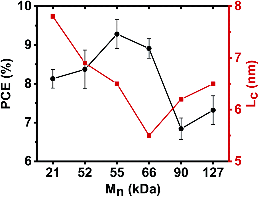 | ||
| Fig. 9 Dependencies of the power conversion efficiency (PCE) of PBDB-T:PNDIBS all-polymer solar cells and the blend crystal coherence length (Lc) on the acceptor polymer PNDIBSMn. | ||
Conclusions
We have synthesized six well-defined number-average molecular weight (Mn) values (21–127 kDa) of the n-type semiconducting biselenophene-naphthalenediimide copolymer (PNDIBS) via direct heteroarylation polymerization (DHAP) and used them to investigated the influence of polymer molecular weight on the morphology, photophysics, charge transport, and photovoltaic properties of all-polymer solar cells (all-PSCs). Both short-circuit current (Jsc) and power conversion efficiency (PCE) of the PBDB-T:PNDIBS blend devices were found to increase with increasing Mn until they peaked at an optimal Mn of 55 kDa and thereafter decreased with further increases in Mn. The maximum and average PCE of 10.2% and 9.3%, respectively, observed at the optimal Mn value of 55 kDa coincided with optimal blend charge transport properties, blend photophysics, and blend morphology at this critical molecular weight. At the optimal Mn, the blend morphology was characterized by a bi-continuous network of 5.5–6.5 nm crystalline domains with predominantly face-on molecular orientations whereas on the higher Mn side a relatively disordered microstructure with larger scale phase separation was evident from 2D-GIWAXS and AFM imaging while a more finely packed crystalline microstructure was observed at 21 kDa. In particular, the observed decrease of photovoltaic parameters at higher Mn could be explained by the larger scale phase separation, decrease in electron mobility, severe bimolecular recombination, and formation of space-charge region. The sensitivity of the all-PSC device efficiency to the active layer thickness was found to depend on the acceptor polymer molecular weight. The PCE of devices at around the optimal Mn was relatively constant with active layer thickness whereas at the higher Mn the efficiency varied significantly with layer thickness, suggesting the potential of using the high molecular weight PNDIBS for semi-transparent all-PSC applications. Overall, the results of this study demonstrate the importance of tuning the molecular weight of the polymer components to optimize the morphology, charge transport, photophysics and efficiency of all-polymer solar cells. The results also provide new insights on structure–property relationships for the n-type semiconducting copolymer PNDIBS.Conflicts of interest
There are no conflicts to declare.Acknowledgements
This work was supported by the NSF (DMR-1708450) and in part by the Office of Naval Research (N00014-17-1-2203). D. K. T. gratefully acknowledges the University of Washington Clean Energy Institute Fellowship. Work at the Laval University was supported by NSERC. The synchrotron radiation based 2D-GIWAXS experiments were performed at the BL46XU of SPring-8 with the support of the Japan Synchrotron Radiation Research Institute (JASRI) (Proposal No. 2018A1744 and No. 2018B1772).References
- C. Lee, S. Lee, G.-U. Kim, W. Lee and B. J. Kim, Chem. Rev., 2019, 119, 8028–8086 CrossRef CAS.
- G. Wang, F. S. Melkonyan, A. Facchetti and T. J. Marks, Angew. Chem., Int. Ed., 2019, 58, 4129–4142 CrossRef CAS.
- Z. Genene, W. Mammo, E. Wang and M. R. Andersson, Adv. Mater., 2019, 31, 1807275 CrossRef.
- H. Benten, D. Mori, H. Ohkita and S. Ito, J. Mater. Chem. A, 2016, 4, 5340–5365 RSC.
- T. Earmme, Y.-J. Hwang, N. M. Murari, S. Subramaniyan and S. A. Jenekhe, J. Am. Chem. Soc., 2013, 135, 14960–14963 CrossRef CAS.
- T. Earmme, Y.-J. Hwang, S. Subramaniyan and S. A. Jenekhe, Adv. Mater., 2014, 26, 6080–6085 CrossRef CAS.
- Y.-J. Hwang, T. Earmme, S. Subramaniyan and S. A. Jenekhe, Chem. Commun., 2014, 50, 10801–10804 RSC.
- Y.-J. Hwang, B. A. E. Courtright, A. S. Ferreira, S. H. Tolbert and S. A. Jenekhe, Adv. Mater., 2015, 27, 4578–4584 CrossRef CAS.
- Y.-J. Hwang, T. Earmme, B. A. E. Courtright, F. N. Eberle and S. A. Jenekhe, J. Am. Chem. Soc., 2015, 137, 4424–4434 CrossRef CAS.
- H. Kang, M. A. Uddin, C. Lee, K.-H. Kim, T. L. Nguyen, W. Lee, Y. Li, C. Wang, H. Y. Woo and B. J. Kim, J. Am. Chem. Soc., 2015, 137, 2359–2365 CrossRef CAS.
- J. Jung, W. Lee, C. Lee, H. Ahn and B. J. Kim, Adv. Energy Mater., 2016, 6, 1600504 CrossRef.
- L. Gao, Z.-G. Zhang, L. Xue, J. Min, J. Zhang, Z. Wei and Y. Li, Adv. Mater., 2016, 28, 1884–1890 CrossRef CAS.
- Z. Li, X. Xu, W. Zhang, X. Meng, W. Ma, A. Yartsev, O. Inganäs, M. R. Andersson, R. A. J. Janssen and E. Wang, J. Am. Chem. Soc., 2016, 138, 10935–10944 CrossRef CAS.
- N. Zhou, A. S. Dudnik, T. I. N. G. Li, E. F. Manley, T. J. Aldrich, P. Guo, H.-C. Liao, Z. Chen, L. X. Chen, R. P. H. Chang, A. Facchetti, M. Olvera de la Cruz and T. J. Marks, J. Am. Chem. Soc., 2016, 138, 1240–1251 CrossRef CAS.
- Z.-G. Zhang, Y. Yang, J. Yao, L. Xue, S. Chen, X. Li, W. Morrison, C. Yang and Y. Li, Angew. Chem. Int. Ed., 2017, 56, 13503–13507 CrossRef CAS.
- Z. Li, X. Xu, W. Zhang, X. Meng, Z. Genene, W. Ma, W. Mammo, A. Yartsev, M. R. Andersson, R. A. J. Janssen and E. Wang, Energy Environ. Sci., 2017, 10, 2212–2221 RSC.
- B. Fan, L. Ying, P. Zhu, F. Pan, F. Liu, J. Chen, F. Huang and Y. Cao, Adv. Mater., 2017, 29, 1703906 CrossRef.
- N. B. Kolhe, H. Lee, D. Kuzuhara, N. Yoshimoto, T. Koganezawa and S. A. Jenekhe, Chem. Mater., 2018, 30, 6540–6548 CrossRef CAS.
- X. Liu, C. Zhang, C. Duan, M. Li, Z. Hu, J. Wang, F. Liu, N. Li, C. J. Brabec, R. A. J. Janssen, G. C. Bazan, F. Huang and Y. Cao, J. Am. Chem. Soc., 2018, 140, 8934–8943 CrossRef CAS.
- X. Xu, Z. Li, J. Wang, B. Lin, W. Ma, Y. Xia, M. R. Andersson, R. A. J. Janssen and E. Wang, Nano Energy, 2018, 45, 368–379 CrossRef CAS.
- X. Xu, Z. Li, W. Zhang, X. Meng, X. Zou, D. Di Carlo Rasi, W. Ma, A. Yartsev, M. R. Andersson, R. A. J. Janssen and E. Wang, Adv. Energy Mater., 2018, 8, 1700908 CrossRef.
- K. D. Deshmukh, R. Matsidik, S. K. K. Prasad, L. A. Connal, A. C. Y. Liu, E. Gann, L. Thomsen, J. M. Hodgkiss, M. Sommer and C. R. McNeill, Adv. Funct. Mater., 2018, 28, 1707185 CrossRef.
- J. Yuan, M. J. Ford, Y. Xu, Y. Zhang, G. C. Bazan and W. Ma, Adv. Energy Mater., 2018, 8, 1703291 CrossRef.
- K. Zhang, R. Xia, B. Fan, X. Liu, Z. Wang, S. Dong, H.-L. Yip, L. Ying, F. Huang and Y. Cao, Adv. Mater., 2018, 30, 1803166 CrossRef.
- H. Yao, F. Bai, H. Hu, L. Arunagiri, J. Zhang, Y. Chen, H. Yu, S. Chen, T. Liu, J. Y. L. Lai, Y. Zou, H. Ade and H. Yan, ACS Energy Lett., 2019, 4, 417–422 CrossRef CAS.
- N. B. Kolhe, D. K. Tran, H. Lee, D. Kuzuhara, N. Yoshimoto, T. Koganezawa and S. A. Jenekhe, ACS Energy Lett., 2019, 4, 1162–1170 CrossRef CAS.
- H. Sun, Y. Tang, C. W. Koh, S. Ling, R. Wang, K. Yang, J. Yu, Y. Shi, Y. Wang, H. Y. Woo and X. Guo, Adv. Mater., 2019, 31, 1807220 CrossRef.
- J. Wu, Y. Meng, X. Guo, L. Zhu, F. Liu and M. Zhang, J. Mater. Chem. A, 2019, 7, 16190–16196 RSC.
- T. Jia, J. Zhang, W. Zhong, Y. Liang, K. Zhang, S. Dong, L. Ying, F. Liu, X. Wang, F. Huang and Y. Cao, Nano Energy, 2020, 72, 104718 CrossRef CAS.
- Y. Wu, S. Schneider, C. Walter, A. H. Chowdhury, B. Bahrami, H.-C. Wu, Q. Qiao, M. F. Toney and Z. Bao, J. Am. Chem. Soc., 2020, 142, 392–406 CrossRef CAS.
- K. Feng, J. Huang, X. Zhang, Z. Wu, S. Shi, L. Thomsen, Y. Tian, H. Y. Woo, C. R. McNeill and X. Guo, Adv. Mater., 2020, 32, 2001476 CrossRef CAS.
- Q. Fan, R. Ma, T. Liu, W. Su, W. Peng, M. Zhang, Z. Wang, X. Wen, Z. Cong, Z. Luo, L. Hou, F. Liu, W. Zhu, D. Yu, H. Yan and E. Wang, Sol. RRL, 2020, 4, 2000142 CrossRef CAS.
- J. Du, K. Hu, L. Meng, I. Angunawela, J. Zhang, S. Qin, A. Liebman-Pelaez, C. Zhu, Z. Zhang, H. Ade and Y. Li, Angew. Chem. Int. Ed., 2020, 59, 15181 CrossRef CAS.
- D. K. Tran, N. B. Kolhe, Y.-j. Hwang, D. Kuzuhara, T. Koganezawa and S. A. Jenekhe, ACS Appl. Mater. Interfaces, 2020, 12, 16490–16502 CrossRef CAS.
- Q. Fan, W. Su, S. Chen, W. Kim, X. Chen, B. Lee, T. Liu, U. A. Mendez-Romero, R. Ma, T. Yang, W. Zhuang, Y. Li, Y. Li, T.-S. Kim, L. Hou, C. Yang, H. Yan, D. Yu and E. Wang, Joule, 2020, 4, 658–672 CrossRef CAS.
- Y. Meng, J. Wu, X. Guo, W. Su, L. Zhu, J. Fang, Z.-G. Zhang, F. Liu, M. Zhang, T. P. Russell and Y. Li, Sci. China Chem., 2019, 62, 845–850 CrossRef CAS.
- Y. Xu, J. Yuan, S. Zhou, M. Seifrid, L. Ying, B. Li, F. Huang, G. C. Bazan and W. Ma, Adv. Funct. Mater., 2019, 29, 1806747 CrossRef.
- S. Lee, Y. Kim, Z. Wu, C. Lee, S. J. Oh, N. T. Luan, J. Lee, D. Jeong, K. Zhang, F. Huang, T.-S. Kim, H. Y. Woo and B. J. Kim, ACS Appl. Mater. Interfaces, 2019, 11, 45038–45047 CrossRef CAS.
- Y. Zhang, Y. Xu, M. J. Ford, F. Li, J. Sun, X. Ling, Y. Wang, J. Gu, J. Yuan and W. Ma, Adv. Energy Mater., 2018, 8, 1800029 CrossRef.
- T. Kim, J.-H. Kim, T. E. Kang, C. Lee, H. Kang, M. Shin, C. Wang, B. Ma, U. Jeong, T.-S. Kim and B. J. Kim, Nat. Commun., 2015, 6, 8547 CrossRef CAS.
- J.-W. Lee, B. S. Ma, J. Choi, J. Lee, S. Lee, K. Liao, W. Lee, T.-S. Kim and B. J. Kim, Chem. Mater., 2020, 32, 582–594 CrossRef CAS.
- J. Choi, W. Kim, S. Kim, T.-S. Kim and B. J. Kim, Chem. Mater., 2019, 31, 9057–9069 CrossRef CAS.
- Q. Zhang, X. Yuan, Y. Feng, B. W. Larson, G. M. Su, Y. Maung Maung, N. Rujisamphan, Y. Li, J. Yuan and W. Ma, Sol. RRL, 2020, 4, 1900524 CrossRef CAS.
- Y. Xu, J. Yuan, S. Liang, J.-D. Chen, Y. Xia, B. W. Larson, Y. Wang, G. M. Su, Y. Zhang, C. Cui, M. Wang, H. Zhao and W. Ma, ACS Energy Lett., 2019, 4, 2277–2286 CrossRef CAS.
- J. Yuan, Y. Zhang, L. Zhou, G. Zhang, H.-L. Yip, T.-K. Lau, X. Lu, C. Zhu, H. Peng, P. A. Johnson, M. Leclerc, Y. Cao, J. Ulanski, Y. Li and Y. Zou, Joule, 2019, 3, 1140–1151 CrossRef CAS.
- Y. Cui, H. Yao, J. Zhang, T. Zhang, Y. Wang, L. Hong, K. Xian, B. Xu, S. Zhang, J. Peng, Z. Wei, F. Gao and J. Hou, Nat. Commun., 2019, 10, 2515 CrossRef.
- S. Liu, J. Yuan, W. Deng, M. Luo, Y. Xie, Q. Liang, Y. Zou, Z. He, H. Wu and Y. Cao, Nat. Photonics, 2020, 14, 300–305 CrossRef CAS.
- J. Yuan, Y. Xu, G. Shi, X. Ling, L. Ying, F. Huang, T. H. Lee, H. Y. Woo, J. Y. Kim, Y. Cao and W. Ma, J. Mater. Chem. A, 2018, 6, 10421–10432 RSC.
- S. Chen, Y. An, G. K. Dutta, Y. Kim, Z.-G. Zhang, Y. Li and C. Yang, Adv. Funct. Mater., 2017, 27, 1603564 CrossRef.
- B. Fan, L. Ying, Z. Wang, B. He, X.-F. Jiang, F. Huang and Y. Cao, Energy Environ. Sci., 2017, 10, 1243–1251 RSC.
- D. Qian, L. Ye, M. Zhang, Y. Liang, L. Li, Y. Huang, X. Guo, S. Zhang, Z. a. Tan and J. Hou, Macromolecules, 2012, 45, 9611–9617 CrossRef CAS.
- T. Bura, J. T. Blaskovits and M. Leclerc, J. Am. Chem. Soc., 2016, 138, 10056–10071 CrossRef CAS.
- A. Robitaille, S. A. Jenekhe and M. Leclerc, Chem. Mater., 2018, 30, 5353–5361 CrossRef CAS.
- T. Bura, S. Beaupre, M.-A. Legare, J. Quinn, E. Rochette, J. T. Blaskovits, F.-G. Fontaine, A. Pron, Y. Li and M. Leclerc, Chem. Sci., 2017, 8, 3913–3925 RSC.
- P.-O. Morin, T. Bura, B. Sun, S. I. Gorelsky, Y. Li and M. Leclerc, ACS Macro Lett., 2015, 4, 21–24 CrossRef CAS.
- M. Wakioka, N. Ichihara, Y. Kitano and F. Ozawa, Macromolecules, 2014, 47, 626–631 CrossRef CAS.
- Y.-J. Hwang, G. Ren, N. M. Murari and S. A. Jenekhe, Macromolecules, 2012, 45, 9056–9062 CrossRef CAS.
- S. Shi, J. Yuan, G. Ding, M. Ford, K. Lu, G. Shi, J. Sun, X. Ling, Y. Li and W. Ma, Adv. Funct. Mater., 2016, 26, 5669–5678 CrossRef CAS.
- Y. Ito, A. A. Virkar, S. Mannsfeld, J. H. Oh, M. Toney, J. Locklin and Z. Bao, J. Am. Chem. Soc., 2009, 131, 9396–9404 CrossRef CAS.
- P. Espinet and A. M. Echavarren, Angew. Chem. Int. Ed., 2004, 43, 4704–4734 CAS.
- W. C. Tsoi, S. J. Spencer, L. Yang, A. M. Ballantyne, P. G. Nicholson, A. Turnbull, A. G. Shard, C. E. Murphy, D. D. C. Bradley, J. Nelson and J.-S. Kim, Macromolecules, 2011, 44, 2944–2952 CrossRef CAS.
- S. Ko, E. T. Hoke, L. Pandey, S. Hong, R. Mondal, C. Risko, Y. Yi, R. Noriega, M. D. McGehee, J.-L. Bredas, A. Salleo and Z. Bao, J. Am. Chem. Soc., 2012, 134, 5222–5232 CrossRef CAS.
- S. Sweetnam, K. R. Graham, G. O. Ngongang Ndjawa, T. Heumuller, J. A. Bartelt, T. M. Burke, W. Li, W. You, A. Amassian and M. D. McGehee, J. Am. Chem. Soc., 2014, 136, 14078–14088 CrossRef CAS.
- R. Noriega, J. Rivnay, K. Vandewal, F. P. V. Koch, N. Stingelin, P. Smith, M. F. Toney and A. Salleo, Nat. Mater., 2013, 12, 1038–1044 CrossRef CAS.
- H. Li, Y.-J. Hwang, B. A. E. Courtright, F. N. Eberle, S. Subramaniyan and S. A. Jenekhe, Adv. Mater., 2015, 27, 3266–3272 CrossRef CAS.
- J. J. Intemann, K. Yao, H.-L. Yip, Y.-X. Xu, Y.-X. Li, P.-W. Liang, F.-Z. Ding, X. Li and A. K. Y. Jen, Chem. Mater., 2013, 25, 3188–3195 CrossRef CAS.
- B. A. E. Courtright and S. A. Jenekhe, ACS Appl. Mater. Interfaces, 2015, 7, 26167–26175 CrossRef CAS.
- G. Ren, C. W. Schlenker, E. Ahmed, S. Subramaniyan, S. Olthof, A. Kahn, D. S. Ginger and S. A. Jenekhe, Adv. Funct. Mater., 2013, 23, 1238–1249 CrossRef CAS.
- C. M. Proctor, M. Kuik and T.-Q. Nguyen, Prog. Polym. Sci., 2013, 38, 1941–1960 CrossRef CAS.
- L. J. A. Koster, V. D. Mihailetchi, R. Ramaker and P. W. M. Blom, Appl. Phys. Lett., 2005, 86, 123509 CrossRef.
- S. R. Cowan, N. Banerji, W. L. Leong and A. J. Heeger, Adv. Funct. Mater., 2012, 22, 1116–1128 CrossRef CAS.
- L. J. A. Koster, V. D. Mihailetchi, H. Xie and P. W. M. Blom, Appl. Phys. Lett., 2005, 87, 203502 CrossRef.
- V. D. Mihailetchi, J. Wildeman and P. W. M. Blom, Phys. Rev. Lett., 2005, 94, 126602 CrossRef CAS.
Footnotes |
| † Electronic supplementary information (ESI) available. See DOI: 10.1039/d0ta08195g |
| ‡ These authors contributed equally. |
| This journal is © The Royal Society of Chemistry 2020 |