
 Open Access Article
 This Open Access Article is licensed under a
 Creative Commons Attribution 3.0 Unported Licence
Bandgap lowering in mixed alloys of Cs2Ag(SbxBi1−x)Br6 double perovskite thin films†‡
Zewei
Li§
*a,
Seán R.
Kavanagh§
 *bcd,
Mari
Napari
e,
Robert G.
Palgrave
b,
Mojtaba
Abdi-Jalebi
f,
Zahra
Andaji-Garmaroudi
a,
Daniel W.
Davies
bd,
Mikko
Laitinen
g,
Jaakko
Julin
g,
Mark A.
Isaacs
bh,
Richard H.
Friend
a,
David O.
Scanlon
bdi,
Aron
Walsh
cj and
Robert L. Z.
Hoye
*c
*bcd,
Mari
Napari
e,
Robert G.
Palgrave
b,
Mojtaba
Abdi-Jalebi
f,
Zahra
Andaji-Garmaroudi
a,
Daniel W.
Davies
bd,
Mikko
Laitinen
g,
Jaakko
Julin
g,
Mark A.
Isaacs
bh,
Richard H.
Friend
a,
David O.
Scanlon
bdi,
Aron
Walsh
cj and
Robert L. Z.
Hoye
*c
aCavendish Laboratory, Department of Physics, University of Cambridge, JJ Thomson Avenue, Cambridge CB3 0HE, UK. E-mail: zl362@cam.ac.uk
bDepartment of Chemistry, University College London, 20 Gordon Street, London WC1H 0AJ, UK. E-mail: sean.kavanagh.19@ucl.ac.uk
cDepartment of Materials, Imperial College London, Exhibition Road, London SW7 2AZ, UK. E-mail: r.hoye@imperial.ac.uk
dThomas Young Centre, University College London, Gower Street, London WC1E 6BT, UK
eZepler Institute for Photonics and Nanoelectronics, University of Southampton, University Road, Southampton SO17 1BJ, UK
fInstitute for Materials Discovery, University College London, Torrington Place, London WC1E 7JE, UK
gDepartment of Physics, University of Jyväskylä, P.O. Box 35, 40014, Finland
hHarwellXPS, Research Complex at Harwell, Harwell Science and Innovation Campus, Didcot, Oxfordshire OX11 0DE, UK
iDiamond Light Source Ltd., Diamond House, Harwell Science and Innovation Campus, Didcot, Oxfordshire OX11 0DE, UK
jDepartment of Materials Science and Engineering, Yonsei University, Seoul 120-749, South Korea
First published on 8th October 2020
Abstract
Halide double perovskites have gained significant attention, owing to their composition of low-toxicity elements, stability in air and long charge-carrier lifetimes. However, most double perovskites, including Cs2AgBiBr6, have wide bandgaps, which limits photoconversion efficiencies. The bandgap can be reduced through alloying with Sb3+, but Sb-rich alloys are difficult to synthesize due to the high formation energy of Cs2AgSbBr6, which itself has a wide bandgap. We develop a solution-based route to synthesize phase-pure Cs2Ag(SbxBi1−x)Br6 thin films, with the mixing parameter x continuously varying over the entire composition range. We reveal that the mixed alloys (x between 0.5 and 0.9) demonstrate smaller bandgaps than the pure Sb- and Bi-based compounds. The reduction in the bandgap of Cs2AgBiBr6 achieved through alloying (170 meV) is larger than if the mixed alloys had obeyed Vegard's law (70 meV). Through in-depth computations, we propose that bandgap lowering arises from the type II band alignment between Cs2AgBiBr6 and Cs2AgSbBr6. The energy mismatch between the Bi and Sb s and p atomic orbitals, coupled with their non-linear mixing, results in the alloys adopting a smaller bandgap than the pure compounds. Our work demonstrates an approach to achieve bandgap reduction and highlights that bandgap bowing may be found in other double perovskite alloys by pairing together materials forming a type II band alignment.
Introduction
Despite the meteoric rise in efficiency of photovoltaics based on lead-halide perovskites,1,2 concerns remain over the toxicity of the lead component.3 Three of the main approaches to find lead-free alternatives are: (a) chemical substitution of Pb2+ with more benign metal cations;4 (b) discovery of materials that could replicate the defect tolerance of the lead-halide perovskites;5,6 and (c) exploration of halide materials that maintain the perovskite crystal structure. The third route has led to extensive work on double perovskites, in which the toxic Pb2+ cation is replaced with a pair of monovalent and trivalent cations (e.g., Ag+ and Bi3+).7–13 Double perovskites, or elpasolites, have the general formula A2B(I)B(III)X6, where A is a monovalent cation (such as Cs+ or CH3NH3+), B(I) a monovalent metal cation (such as Na+, Cu+, Ag+ or Au+), B(III) a trivalent metal cation (usually Sb3+, Bi3+ or In3+) and X a halide anion (Cl−, Br− or I−).7,13–15 Calculations have shown that the bandgap can be tuned over a wide range by changing the species in each atomic site. There has been particular focus on Cs2AgBiBr6 for photovoltaic applications, and several groups have demonstrated long charge-carrier lifetimes, which can exceed a microsecond.13,16,17 Photovoltaic devices with Cs2AgBiBr6 have demonstrated high external quantum efficiencies reaching 60%,18 with stable performance over hundreds of hours in ambient air.19 These promising charge transport properties, coupled with the improved stability of Cs2AgBiBr6 over lead-halide perovskites, have led to the material also being considered for photocatalytic applications.20,21However, the potential of Cs2AgBiBr6 for photovoltaic and photocatalytic applications is limited by the wide bandgap (2.1–2.3 eV) and its indirect nature, which limit light absorption.12,13,20–23 Efforts to achieve a smaller and more direct bandgap have involved alloying with Tl, but this is more toxic than Pb.8,24 Alloying Cs2AgBiBr6 with the substantially less toxic Sb was also shown to be effective, but led to a smaller reduction in bandgap than Tl alloying.25–27 In part, this was because the Sb-based double perovskite itself (Cs2AgSbBr6) has a wide bandgap of 1.9–2.1 eV.11,15 Another factor was that only a maximum of 37.5% Sb could be introduced through powder melt synthesis, limiting the extent of bandgap reduction.25 Intriguingly, mixed Cs2Ag(SbxBi1−x)Br6 alloys have exhibited a non-linear reduction in the bandgap, i.e., bandgap bowing, with increasing Sb content.25,27 Bandgap bowing has also been found in Pb/Sn perovskite alloys, and, in this case, the bowing is pronounced, such that the mixed alloy exhibits a smaller bandgap than either of the pure Pb- or Sn-based compounds.28–30 An important question would be whether a similar phenomenon occurs in Cs2Ag(SbxBi1−x)Br6 alloys.
So far, there is a lack of understanding of the extent of bandgap bowing in Sb–Bi double perovskite alloys and whether the mixed compositions could exhibit a smaller bandgap than the pure compounds. This requires the full composition range in Cs2Ag(SbxBi1−x)Br6 alloys to be synthesized. However, synthesizing phase-pure Cs2AgSbBr6 is challenging, particularly in thin film form. This is due to the high formation energy of Cs2AgSbBr6 and the small ionic radius of Sb3+ relative to Bi3+.31 Recently, Liu et al. synthesized thin films of Cs2Ag(SbxBi1−x)Br6 alloys by dipping their substrates in a heated solution of the precursor salts dissolved in dimethyl sulfoxide (DMSO).27 But they were only able to achieve up to 75% Sb alloying and were not able to synthesize the pure Sb-based compound. Colloidal nanocrystal synthesis routes have been found to be more successful in growing less thermodynamically-favored compounds (e.g., iodide-based double perovskites, which have a positive heat of formation). Yang et al. recently developed a route to grow Cs2AgSbBr6 nanocrystals.31 But it is also desirable to achieve phase-pure Cs2AgSbBr6 as bulk thin films, which do not have carriers confined within individual grains, as is the case for nanocrystals bound with long-chain ligands.
In this work, we achieved the synthesis of Sb–Bi double perovskite alloys over the entire composition range in thin film form. We found that the mixed alloys have a lower bandgap than the pure Bi- and Sb-based double perovskites, with similar pronounced nonlinear bandgap behavior to that found in lead–tin perovskite alloys.28–30 Through X-ray diffraction (XRD) and Rutherford Backscattering Spectrometry (RBS), we found all films to be phase-pure, with the thin film composition in the bulk matching the ratio of elements in the precursor solution. We used Photothermal Deflection Spectroscopy (PDS) to accurately determine how the indirect bandgap and electronic disorder in Sb–Bi double perovskite alloys changed with composition. The electronic structure and band positions were calculated by Density Functional Theory (DFT) to provide insight into the origins of the bandgap lowering observed in the Sb–Bi double perovskite alloys.
Results and discussion
Synthesis and verification of composition
Cs2Ag(SbxBi1−x)Br6 thin films were synthesized by solution processing. The CsBr, AgBr, SbBr3 and BiBr3 precursors were mixed according to their stoichiometric ratio in DMSO with a concentration of 0.5 mol L−1. In contrast to the dipping method used by Liu et al.,27 we used a lower annealing temperature and shorter annealing time (detailed in the Experimental section in the ESI‡), which may have contributed to the successful synthesis of phase-pure Cs2AgSbBr6. Photographs of the films (approx. 200 nm thickness in all cases) are shown in Fig. 1a, and it was observed that the mixed compositions have a deeper color. To determine the bulk composition of the films, we performed RBS measurements (Fig. 1b and Table 1). It was found that the Sb/Bi ratio from the RBS measurements matched the stoichiometry in the precursor solution, deviating from the nominal precursor stoichiometry by up to 2.1 percentage points (Table 1). Since the Sb RBS peak is buried between two other peaks (Ag and Cs, see Fig. S1, ESI‡), the fitting and statistical uncertainties are high when the Sb concentration is low. These deviations could arise from uncertainties in the RBS measurement, as well as errors in preparing the precursor solution. These measurements therefore indicate that there is no change in the bulk composition of the thin films during crystallization. However, the presence of phase-impurities in the films below the percent-level could not be excluded. | ||
| Fig. 1 (a) Photographs of the Cs2Ag(SbxBi1−x)Br6 films on glass under ambient lighting, with a thickness of approximately 200 nm. The Sb percentage labelled is that in the precursor solution. (b) Measurement of the bulk composition of Cs2Ag(SbxBi1−x)Br6 films with Rutherford Backscattering Spectrometry (fitting in Fig. S1, ESI‡). | ||
| Nominal Sb/(Sb + Bi) in precursor solution | RBS | |||||
|---|---|---|---|---|---|---|
| Cs/at% | Ag/at% | Sb/at% | Bi/at% | Br/at% | Sb/(Sb + Bi) in film | |
| 100% | 20.5 | 10.1 | 9.5 | 0 | 59.5 | 100% |
| 90% | 19.6 | 10.1 | 9.2 | 1.2 | 60.0 | 88.5% |
| 70% | 19.6 | 10.5 | 7.5 | 3.2 | 59.4 | 70.1% |
| 50% | 19.5 | 10.6 | 5.5 | 5.2 | 59.2 | 51.4% |
| 20% | 19.8 | 10.4 | 2.3 | 8.1 | 59.4 | 22.1% |
| 0% | 19.8 | 10.0 | 0 | 10.1 | 60.1 | 0% |
Crystal structure and phase purity
The phase-purity of the films was determined through XRD measurements (Fig. 2a). Cs2AgSbBr6 and Cs2AgBiBr6 have the same cubic structure and space group (Fm![[3 with combining macron]](https://www.rsc.org/images/entities/char_0033_0304.gif) m). The lattice constants were found to be 11.184 Å for Cs2AgSbBr6 and 11.255 Å for Cs2AgBiBr6, with a continuous variation between these extremes through the alloying range, as could be seen from the continuous shift in peak positions (Fig. 2b and 3d). Common phase impurities for the Sb–Bi double perovskites are Cs3Bi2Br9 and Cs3Sb2Br9. Both impurities have almost the same diffraction patterns with their double perovskite counterparts, but one of the main differences is a peak from Cs3Bi2Br9 at 8.95°, or from Cs3Sb2Br9 at 9.10°.32 Neither impurity peaks were found to be present here. However, these XRD measurements were taken using a 1D linescan, and it is possible that the impurity peaks were not detected due to preferred orientation. We therefore performed 2D XRD measurements (Fig. S2, ESI‡). We synthesized the whole alloying range of double perovskite thin films and intentionally induced a Cs3(Bi,Sb)2Br9 phase impurity to the films with 50% Sb. From the 2D XRD patterns, we found that the diffraction peak should be detectable by the 1D linescan if it is present. Therefore, the absence of any phase-impurities in the 1D XRD patterns in Fig. 2a shows the films to be phase-pure.
m). The lattice constants were found to be 11.184 Å for Cs2AgSbBr6 and 11.255 Å for Cs2AgBiBr6, with a continuous variation between these extremes through the alloying range, as could be seen from the continuous shift in peak positions (Fig. 2b and 3d). Common phase impurities for the Sb–Bi double perovskites are Cs3Bi2Br9 and Cs3Sb2Br9. Both impurities have almost the same diffraction patterns with their double perovskite counterparts, but one of the main differences is a peak from Cs3Bi2Br9 at 8.95°, or from Cs3Sb2Br9 at 9.10°.32 Neither impurity peaks were found to be present here. However, these XRD measurements were taken using a 1D linescan, and it is possible that the impurity peaks were not detected due to preferred orientation. We therefore performed 2D XRD measurements (Fig. S2, ESI‡). We synthesized the whole alloying range of double perovskite thin films and intentionally induced a Cs3(Bi,Sb)2Br9 phase impurity to the films with 50% Sb. From the 2D XRD patterns, we found that the diffraction peak should be detectable by the 1D linescan if it is present. Therefore, the absence of any phase-impurities in the 1D XRD patterns in Fig. 2a shows the films to be phase-pure.
 | ||
| Fig. 2 (a) XRD pattern of the Cs2Ag(SbxBi1−x)Br6 films over the composition series. The reference patterns of Cs2AgSbBr6 and Cs2AgBiBr6 calculated from their crystallographic information files are denoted as Sb Ref and Bi Ref respectively.12,15 (b) Full width half maximum (FWHM) of the (022) peak for different compositions. (c) FWHM of different diffraction peaks and the average grain size calculated using the Scherrer equation for different compositions. | ||
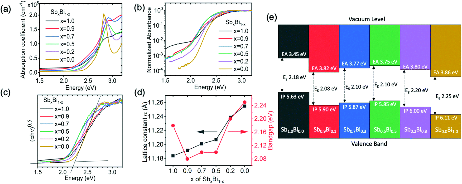 | ||
| Fig. 3 Measurements of the bandgap of Cs2Ag(SbxBi1−x)Br6 films. (a) Absorption coefficient determined from transmittance and reflectance measurements of films deposited on glass substrates. (b) Normalized absorbance measured by PDS for films deposited on quartz substrates. (c) Tauc plot from PDS measurements. (d) Bandgap and lattice parameter of double perovskite films plotted against the Sb content in the precursor solution. The lattice parameter was acquired by fitting the XRD measurements (Fig. 2a). The bandgap was obtained from the Tauc plot constructed from the PDS data in part c. (e) Band positions of Cs2Ag(SbxBi1−x)Br6 compounds measured by ultraviolet and X-ray photoemission spectroscopy. Details of how measurements were taken and processed, the spectra fitted, and the fitted values are shown in the ESI.‡ | ||
The diffraction patterns also showed no peak splitting, but the full width at half maximum (FWHM) of the pure Sb-based double perovskite and mixed alloys were larger than the Bi-based double perovskite (Fig. 2b and c). This could either be due to smaller grains or small amounts of phase segregation that could not be resolved. Scanning Electron Microscopy (SEM) measurements of the films showed that the Sb-based double perovskites and mixed alloys have smaller and less well-defined grains than the pure Bi-based double perovskite (Fig. S3, ESI‡), which is consistent with the larger FWHM in the diffraction patterns of Sb containing films. These XRD and SEM measurements, together with the RBS measurements matching the stoichiometry of the precursor solutions, are consistent with the alloys being homogeneous.
We note that previous works have reported that mixed Sb–Bi double perovskite alloys with high Sb contents have marginally lower stability. For example, Liu et al. found that Cs2Ag(SbxBi1−x)Br6 thin films with x = 0.75 had AgBr and CsAgBr2 decomposition products after 4 h annealing at 250 °C.27 However, the diffraction peaks of these phases were small compared to the main double perovskite peaks, showing the degree of degradation to be small.27 Sb–Bi double perovskites with lower Sb contents have been found to have comparable thermal and environmental stability as Cs2AgBiBr6.25,27 Furthermore, the reported stability of mixed Sb–Bi double perovskites is significantly improved over MAPbI3 thin films, which degrades in ambient air within 5 days33 and decomposes to form a significant fraction of PbI2 after 35 min at 150 °C.34
Absorption, bandgap and band positions
Standard optical transmittance and reflectance measurements (using a UV-visible spectrophotometer with an integrating sphere) were used to determine the absorption coefficient of the double perovskite thin films (Fig. 3a). All films showed a slow increase in the absorption coefficient for photon energies > 2 eV, before rising sharply to >105 cm−1 at >2.6 eV. An absorption coefficient exceeding 105 cm−1 at >2.6 eV is characteristic of a direct band-to-band transition. Both Cs2AgBiBr6 and Cs2AgSbBr6 have indirect bandgaps due to the effects of the Ag d orbitals at the band-edges, and the alloys are also expected to have indirect bandgaps.8 Therefore, to determine the indirect bandgap, we investigated the absorption onset in the lower photon energy range (i.e., between 2–2.6 eV), leaving the discussion of the absorption in the higher photon energy range to later in the paper. We observed that the alloys with 70–90% Sb showed a lower-energy absorption onset than the pure Sb- and Bi-based films. However, the indirect bandgaps resulted in the absorption coefficients being small close to the band-edge, making it difficult to accurately determine the bandgap from standard transmittance and reflectance measurements. Therefore, we performed PDS measurements, which are sensitive to the absorbance 3–4 orders below the band-edge (operating details in the Experimental section, ESI‡).A consequence of the high sensitivity to low absorbance is that the measurements in PDS saturate for high absorbance at >2.6 eV (Fig. 3b), and the peaks in the absorption coefficient seen in Fig. 3a are not observed in the PDS measurements plotted on a semi-logarithmic scale (see later in the paper for a discussion of these peaks). The normalized absorbance from PDS measurements at the band edge (in the range of 2–2.3 eV) is approximately 3 orders of magnitude lower than the absorbance at 2.6 eV, where the absorption coefficient is >105 cm−1 (Fig. 3a). Thus, the absorption coefficient at the band edge should be on the order of 102 cm−1. We note that silicon, which is a typical indirect bandgap material, has an absorption coefficient of 102 cm−1 at the band edge.35,36
The absorption plots shown in Fig. 3b do qualitatively indicate an exponentially increasing absorption coefficient versus energy, which appears linear on a semi-logarithmic plot. The double perovskites with x ranging from 0 to 0.7 have similar slopes in their absorption onsets when plotted on a semi-logarithmic scale. For x = 0.9 and the pure Sb-based compound, the slopes are shallower. Increasing the fraction of Sb (x) from 0 (pure Bi) to 0.5 reveals a red-shift in the absorption onset. The double perovskites with x = 0.7 and x = 0.9 all have similar absorption onsets to the material with x = 0.5. These mixed alloys with x = 0.5–0.9 all have absorption onsets that are red-shifted to the pure Sb-based compound, as well as the pure Bi-based compound. Therefore, alloys with 50–90% Sb demonstrate smaller bandgaps than either of the pure end double perovskites. To extract numerical values of the bandgap and quantify their variation with composition, we fitted the PDS absorbance data using a Tauc plot, which is a plot of (αhν)1/n against hν. The rationale can be seen from eqn (1)
| (αhν)1/n = A(hν − Eg) | (1) |
In addition, we measured the band positions of Cs2Ag(SbxBi1−x)Br6 over the full composition range through photoemission spectroscopy (PES; Fig. 3e). Details of how the ionization potential and electron affinity were obtained are given in the Experimental section of the ESI.‡ The fitted spectra are given in Fig. S5–S11, ESI.‡ These measurements showed that when alloying Bi into Cs2AgSbBr6, the electron affinity increased from 3.45 eV to ∼3.8 eV and remained at approximately this value for the mixed alloys, which is similar to the electron affinity of Cs2AgBiBr6 (3.86 eV). The ionization potential also increased when adding Bi to Cs2AgSbBr6, but to a lesser extent than the change in the electron affinity, hence the reduction in the bandgap. The ionization potential remained at approximately 5.9 eV for x = 0.9 down to x = 0.5, before increasing to 6.11 eV for x = 0 (Fig. 3e). Overall, the band positions of the Cs2Ag(SbxBi1−x)Br6 alloys are compatible with the common charge transport layers for photovoltaic devices.37 But like most other Bi-based compounds,38 Cs2Ag(SbxBi1−x)Br6 has high ionization potentials. Achieving high open-circuit voltages will therefore require the development of hole transport layers with high work functions.
Electronic structure and bandgap lowering mechanism
To understand the atomistic origin of the bandgap lowering in the Sb–Bi double perovskites, calculations of the electronic structure were performed. The band structure and density of states for pure Sb and Bi double perovskites are shown in Fig. 4a–d. In agreement with previous literature, as well as our optical measurements in Fig. 3, both Cs2AgSbBr6 and Cs2AgBiBr6 were found to have an indirect bandgap,8,15,25 with the valence band maximum (VBM) located at the X point and the conduction band minimum (CBM) at the L point in reciprocal space. Using relativistic hybrid density functional theory (HSE06 including spin–orbit coupling), the indirect bandgap and first direct transition of Cs2AgSbBr6 were calculated to be 1.37 and 2.60 eV, respectively. Analysis of the electron band orbital character revealed the conduction band states to be dominated by anti-bonding Sb 5p–Br 4p interactions, while the valence band states primarily arise from Sb 5s, Ag 4d and Br 4p orbital interactions. The Cs+ cations act as spectator ions, as noted in the literature,39 with a relatively large nearest-neighbor-ion distance to Br−. | ||
| Fig. 4 (a) Orbital-projected band structure of Cs2AgSbBr6. (b) Orbital-projected band structure of Cs2AgBiBr6. (c) Electronic density of states of Cs2AgSbBr6. (d) Electronic density of states of Cs2AgBiBr6. (e) Electron band alignment of Cs2AgSbBr6 and Cs2AgBiBr6. CBO = Conduction Band Offset, VBO = Valence Band Offset. (f) Calculated optical absorption plots of Cs2AgSbBr6 (blue) and Cs2AgBiBr6 (orange). Dashed vertical lines indicate the positions of optical absorption onset, corresponding to the direct band transitions of 2.60 eV for Cs2AgSbBr6 and 2.49 eV for Cs2AgBiBr6. Note that only vertical transitions are accounted for in this calculation, and the absorption from indirect transitions are not shown. | ||
Likewise, the indirect bandgap and direct transition of Cs2AgBiBr6 were calculated to be 1.77 and 2.49 eV, respectively. Due to the stronger spin–orbit coupling of the Bi 6p orbitals, the direct bandgap of Cs2AgBiBr6 is slightly reduced from that of Cs2AgSbBr6, despite a larger fundamental gap, and is located at a different point in reciprocal space (X = (0.5, 0, 0.5), cf. b = (0.5, 0.38, 0.62) for Cs2AgSbBr6). Similarly, the conduction band states are dominated by anti-bonding interactions between the trivalent pnictogen cation (Bi 6p) and the halide anion (Br 4p) orbitals, while the valence band states primarily arise from Bi 6s, Ag 4d and Br 4p orbital interactions. Notably, the larger band gap of Cs2AgBiBr6 relative to Cs2AgSbBr6 is an interesting exception to the typical trend of decreasing bandgap upon atomic substitution with heavier members from the same periodic group, which has been observed for other perovskite materials.11,40,41
To delve closer to the origin of bandgap lowering, the ‘natural’ band offset of the two double perovskite materials was calculated following the alignment procedure of Butler et al.,42 with the resulting electron band alignment diagram shown in Fig. 4e. Our investigations indicate a type II ‘staggered gap’ alignment, with a valence band offset (VBO) of 0.75 eV and a conduction band offset (CBO) of 0.34 eV (Cs2AgSbBr6 above Cs2AgBiBr6 in both cases). Typically, the energies of valence electrons become less negative as one moves down a group in the periodic table, corresponding to a decrease in ionization energies. However, for Bi3+ and Sb3+, this is not the case, with the Bi3+ 6s2 lone pair being lower in energy than the Sb3+ 5s2 lone pair.43 This is a result of the relativistic contraction of the Bi 6s orbital, due to its large atomic number, resulting in a more localized, lower-energy valence s orbital, compared to Sb 5s.44
Consequently, the more-diffuse, higher-energy Sb 5s2 lone-pair has a stronger interaction with the Ag 4d and Br 4p orbitals, due to a reduced energy separation of the bonding orbitals (Fig. S12, ESI‡). This produces both greater dispersion in the valence band and a higher VBM, as shown in Fig. 4e. In a similar manner, the elevated position of the CBM in Cs2AgSbBr6 can be understood by considering the ionization energies and ionic orbital energies. While the first ionization energy of Sb is indeed larger than that of Bi, the third ionization energy (corresponding to the removal of a p electron from Sb2+/Bi2+) is in fact 0.3 eV lower for Sb than for Bi,43 indicating higher energy cationic p states. When the pnictogen elements are in the +3 oxidation state, as is the case in these materials, the third ionization energy provides an improved estimate for the energy of the unoccupied p orbitals. Hence, we argue that, in the +3 formal charge state, the Sb valence p orbitals are in fact higher in energy than those of Bi, suggesting a higher energy CBM for Cs2AgSbBr6, as witnessed in our investigations.
The origins of bandgap bowing in semiconductor alloys are typically due to chemical effects (e.g., differences in electronegativity), local size-mismatch effects or changes in the lattice parameter.45–47 For the Pb–Sn perovskite alloy system, Im et al. attributed bandgap bowing to the combined effect of spin–orbit coupling and composition-induced phase change.30 Snaith and coworkers proposed that the short range ordering of preferred atomic scale clusters allow the bandgap of the mixed alloy to be below that of both pure compounds.29 In contrast, Stevanović and coworkers found that the strong nonlinearity in bandgap was primarily due to the mismatch in energy between s and p atomic orbitals of Pb and Sn.28 The Pb–Sn alloys have a higher VBM dominated by Sn-5s and I-5p orbitals and lower CBM dominated by Pb-6p and I-5p orbitals. They found that spin–orbit coupling, structure changes and short-range ordering did not have a significant effect on bandgap bowing, and proposed that a homogeneous structure would have improved stability over a structure with short range ordering.
In the case of Cs2Ag(SbxBi1−x)Br6, we propose that the type II staggered gap alignment between the pure compounds allows for the non-linear mixing of electronic states such that bandgaps lower than that of either pure material are obtained (Fig. 4e). Upon addition of Bi to the pure Sb double perovskite, the conduction band will be lowered because the CBM wavefunction amplitude is preferentially allocated to the Bi sites, producing a ‘Bi-like’, lower-energy conduction band state. The presence of Bi will also enhance spin–orbit coupling, further reducing the energy of the CBM. On the other hand, the highest energy valence band state will remain ‘Sb-like’, with greater wavefunction amplitude at the Sb sites yielding a VBM only slightly below that of the pure Sb material. This mixing of electronic states in the alloys to produce a low-energy CBM, dominated by Bi–Br interactions, and a high-energy VBM, dominated by Sb–Ag–Br interactions, produces bandgaps in the double perovskite alloys which are lower than that of either pure material. Indeed, this prediction is supported by electronic structure calculations for the alloys (assuming a uniform atomic distribution), which show reduced bandgaps due to the expected orbital mixing at the band edges (Fig. S13–S15 and Table S3, ESI‡). These predictions are further supported by the experimentally-determined band positions of the Cs2Ag(SbxBi1−x)Br6 compounds (Fig. 3e), which show the electron affinities of the mixed alloys to be close to Cs2AgBiBr6. The ionization potentials of the mixed alloys with x = 0.5–0.9 are in between those of the pure compounds. This accounts for the reduction in their bandgap compared to Cs2AgBiBr6. The reduction in the bandgaps of the x = 0.5–0.9 mixed alloys compared to Cs2AgSbBr6 are due to the increase in ionization potential being smaller than the increase in electron affinity when Bi is added to Cs2AgSbBr6, as discussed earlier.
Notably, this combination of a low-energy CBM with a high-energy VBM is expected to allow for enhanced doping and hence increased carrier concentrations in the alloy, relative to the pure materials.48–50 In particular, the raised VBM, relative to pure Cs2AgBiBr6 (which has been reported as intrinsically p-type),10,16,51 should allow for greater hole carrier concentrations in the reduced-bandgap alloy. This is supported by our X-ray photoemission spectroscopy measurements, which show a reduction in the valence band to Fermi level offset when Sb is alloyed into Cs2AgBiBr6, showing the materials to become more p-type (Table S1, ESI‡).
As the alloy mixing parameter x approaches extreme values (x → 0 or x → 1), the ability of the band extrema states to simultaneously adopt Bi and Sb character is diminished, hence the bandgap increases toward the pure double perovskite values. Therefore, we propose that this orbital-mixing behavior, facilitated by the type II bandgap alignment, is the origin of the non-linear, non-monotonic variation in bandgap with composition in the Sb–Bi double perovskite system.
Another possible contribution to bandgap bowing is volume deformation, whereby variation in the lattice constant upon alloying results in non-linear transformation of the electronic structure.28 This mechanism, however, more commonly dominates in alloys involving more chemically-distinct materials than is the case here. Moreover, due to the small positive bandgap deformation potentials calculated for the Sb and Bi compounds (ΔEg ∼ 0.02 eV), we rule out this mechanism. Relative to the experimentally-observed bowing (∼0.1 eV, Fig. 3d), volume distortion alone is not the origin of bandgap bowing in this alloy system.
Finally, we return to discuss the sharp peak in the absorption coefficient of the films at >2.6 eV (Fig. 3a). This is especially evident for Cs2AgBiBr6. Previous work attributed the sharp absorption peak in Cs2AgBiBr6 to an exciton associated with the direct transition.26,52–55 However, there is also the possibility that these features in the pure compounds and mixed alloys are due to a narrow density of states at the band-edges. To explore this possibility, we computed the absorption spectra for Cs2AgSbBr6 and Cs2AgBiBr6 without excitonic effects (Fig. 4f). These spectra were broadened by convoluting with a Gaussian peak with a FWHM of 0.15 eV. For both materials, the calculated absorption spectra exhibit peaks at 2.8 eV, in agreement with the experimental measurements. These peaks arise from the relatively-weak dispersion of the electron bands at the CBM and VBM of the materials (Fig. 4a and b), yielding peaks in both the density of states (Fig. 4c and d) and thus the optical absorption (Fig. 4f). This strongly suggests that the peaks observed in the experimental UV-visible measurements are the result of direct transitions between the relatively-flat electron bands. That said, the exciton binding energy of Cs2AgBiBr6 was calculated to be 167 meV within effective mass theory, which is sufficiently large that stable exciton formation is possible in these systems.
Curiously, the computed absorption spectrum for Cs2AgSbBr6 shows a distinct absorption peak (Fig. 4f), whereas the measured peak from UV-visible spectrophotometry became less distinct with increasing Sb content, until there was barely an observable peak for the pure Sb-based compound (Fig. 3a). This may have been due a ‘smearing out’ of the absorption peak due to structural disorder.56–58 We calculated the absorption spectra for the pure Sb-based compound convoluted with Gaussian peaks with wider FWHM (0.2 eV, 0.3 eV, 0.4 eV; Fig. S16, ESI‡). These show that the peak becomes indistinguishable when broadening is large, as witnessed experimentally and consistent with the PDS measurements. Thus, peak broadening as a result of disorder leads to the observed ‘smeared-out’ absorption spectrum in Fig. 3a.
Conclusions
In conclusion, we successfully synthesized phase-pure Cs2AgSbBr6 thin films, as well as Cs2Ag(SbxBi1−x)Br6 with x varying over the full composition range. In doing so, we found that the mixed double perovskites with x between 0.5 and 0.9 to have the smallest bandgaps, lower than those of the pure compounds. From the electronic band alignment, we found that the origin of bandgap bowing in this double perovskite alloy is due to chemical rather than structural effects. The type II band alignment between Cs2AgBiBr6 and Cs2AgSbBr6, in combination with non-linear mixing of the electronic states, results in the alloy having smaller bandgaps than either pure material. Our work demonstrates a novel route to reduce the bandgap of Cs2AgBiBr6 and Cs2AgSbBr6, which could be generalized to other halide double perovskites. That is, we propose that alloys formed from compounds with a type II band alignment could exhibit similar bandgap lowering. This may prove crucial for improving the suitability of double perovskites for photovoltaic and photocatalytic applications.Author contributions
Z. L. synthesized the Sb–Bi double perovskite thin films, took photographs, and performed 1D XRD, SEM and UV-visible spectrophotometry measurements. S. R. K. performed the theoretical calculations and analyzed the results, along with D. W. D., D. O. S. and A. W. M. N. analyzed the RBS results, which were collected by M. L. and J. J. R. G. P. measured the 2D XRD data. M. A.-J. and Z. A.-G. measured and analyzed the PDS data. M. I. performed the PES measurements. R. H. F. supervised Z. L. and contributed to the discussion. R. L. Z. H. conceived of the project and supervised the work. All authors discussed the results and contributed to writing the paper.Conflicts of interest
There are no conflicts of interest to declare.Acknowledgements
Z. L. would like to thank Cambridge Trust and Chinese Scholarship Council for financial support. S. R. K. acknowledges funding from the EPSRC Centre for Doctoral Training in Advanced Characterisation of Materials (CDT-ACM) (EP/S023259/1), the use of the UCL Grace High Performance Computing Facility (Grace@UCL), the Imperial College Research Computing Service (DOI: 10.14469/hpc/2232), and associated support services in the completion of this work. Via membership of the UK's HEC Materials Chemistry Consortium, which is funded by EPSRC (EP/L000202), this work also used the UK Materials and Molecular Modelling (MMM) Hub for computational resources, which is partially funded by the EPSRC (EP/P020194). R. L. Z. H. acknowledges support from the Royal Academy of Engineering under the Research Fellowship Programme (No. RF\201718\1701), the Isaac Newton Trust (Minute 19.07(d)), and the Kim and Juliana Silverman Research Fellowship at Downing College, Cambridge. M. A.-J. thanks Cambridge Materials Limited, Wolfson College, University of Cambridge and EPSRC (grant no. EP/M005143/1) for their funding and technical support. For the RBS experiments, the authors acknowledge the RADIATE project under the Grant Agreement 824096 from the EU Research and Innovation programme HORIZON 2020. The X-ray photoelectron (XPS) and UV photoelectron (UPS) data collection was performed at the EPSRC National Facility for XPS (“HarwellXPS”), operated by Cardiff University and UCL, under Contract No. PR16195.References
- L. Yang, A. T. Barrows, D. G. Lidzey and T. Wang, Rep. Prog. Phys., 2016, 79, 026501 CrossRef.
- H. S. Jung and N. G. Park, Small, 2015, 11, 10–25 CrossRef CAS.
- A. Babayigit, A. Ethirajan, M. Muller and B. Conings, Nat. Mater., 2016, 15, 247–251 CrossRef CAS.
- S. Nagane, D. Ghosh, R. L. Z. Hoye, B. Zhao, S. Ahmad, A. B. Walker, M. Saiful Islam, S. Ogale and A. Sadhanala, J. Phys. Chem. C, 2018, 122, 5940–5947 CrossRef CAS.
- R. E. Brandt, J. R. Poindexter, P. Gorai, R. C. Kurchin, R. L. Z. Hoye, L. Nienhaus, M. W. B. Wilson, J. A. Polizzotti, R. Sereika, R. Žaltauskas, L. C. Lee, J. L. Macmanus-Driscoll, M. Bawendi, V. Stevanović and T. Buonassisi, Chem. Mater., 2017, 29, 4667–4674 CrossRef CAS.
- A. Walsh, D. O. Scanlon, S. Chen, X. G. Gong and S. H. Wei, Angew. Chem. Int. Ed., 2015, 54, 1791–1794 ( Angew. Chem. , 2015 , 127 , 1811–1814 ) CrossRef CAS.
- F. Wei, Z. Deng, S. Sun, F. Zhang, D. M. Evans, G. Kieslich, S. Tominaka, M. A. Carpenter, J. Zhang, P. D. Bristowe and A. K. Cheetham, Chem. Mater., 2017, 29, 1089–1094 CrossRef CAS.
- C. N. Savory, A. Walsh and D. O. Scanlon, ACS Energy Lett., 2016, 1, 949–955 CrossRef CAS.
- F. Wei, Z. Deng, S. Sun, F. Xie, G. Kieslich, D. M. Evans, M. A. Carpenter, P. Bristowe and T. Cheetham, Mater. Horiz., 2016, 3, 328–332 RSC.
- Z. Xiao, W. Meng, J. Wang and Y. Yan, ChemSusChem, 2016, 9, 2628–2633 CrossRef CAS.
- G. Volonakis, M. R. Filip, A. A. Haghighirad, N. Sakai, B. Wenger, H. J. Snaith and F. Giustino, J. Phys. Chem. Lett., 2016, 7, 1254–1259 CrossRef CAS.
- E. T. McClure, M. R. Ball, W. Windl and P. M. Woodward, Chem. Mater., 2016, 28, 1348–1354 CrossRef CAS.
- A. H. Slavney, T. Hu, A. M. Lindenberg and H. I. Karunadasa, J. Am. Chem. Soc., 2016, 138, 2138–2141 CrossRef CAS.
- J. Luo, X. Wang, S. Li, J. Liu, Y. Guo, G. Niu, L. Yao, Y. Fu, L. Gao, Q. Dong, C. Zhao, M. Leng, F. Ma, W. Liang, L. Wang, S. Jin, J. Han, L. Zhang, J. Etheridge, J. Wang, Y. Yan, E. H. Sargent and J. Tang, Nature, 2018, 563, 541–545 CrossRef CAS.
- F. Wei, Z. Deng, S. Sun, N. T. P. Hartono, H. L. Seng, T. Buonassisi, P. D. Bristowe and A. K. Cheetham, Chem. Commun., 2019, 55, 3721–3724 RSC.
- R. L. Z. Hoye, L. Eyre, F. Wei, F. Brivio, A. Sadhanala, S. Sun, W. Li, K. H. L. Zhang, J. L. MacManus-Driscoll, P. D. Bristowe, R. H. Friend, A. K. Cheetham and F. Deschler, Adv. Mater. Interfaces, 2018, 5, 1800464 CrossRef.
- D. Bartesaghi, A. H. Slavney, M. C. Gélvez-Rueda, B. A. Connor, F. C. Grozema, H. I. Karunadasa and T. J. Savenije, J. Phys. Chem. C, 2018, 122, 4809–4816 CrossRef CAS.
- E. Greul, M. L. Petrus, A. Binek, P. Docampo and T. Bein, J. Mater. Chem. A, 2017, 5, 19972–19981 RSC.
- F. Igbari, R. Wang, Z. K. Wang, X. J. Ma, Q. Wang, K. L. Wang, Y. Zhang, L. S. Liao and Y. Yang, Nano Lett., 2019, 19, 2066–2073 CrossRef CAS.
- L. Zhou, Y. F. Xu, B. X. Chen, D. Bin Kuang and C. Y. Su, Small, 2018, 14, 1703762 CrossRef.
- Z. Zhang, Y. Liang, H. Huang, X. Liu, Q. Li, L. Chen and D. Xu, Angew. Chem. Int. Ed., 2019, 58, 7263–7267 ( Angew. Chem. , 2019 , 131 , 7341–7345 ) CrossRef CAS.
- M. R. Filip, S. Hillman, A. A. Haghighirad, H. J. Snaith and F. Giustino, J. Phys. Chem. Lett., 2016, 7, 2579–2585 CrossRef CAS.
- H. Huang, B. Pradhan, J. Hofkens, M. B. J. Roeffaers and J. A. Steele, ACS Energy Lett., 2020, 5, 1107–1123 CrossRef CAS.
- A. H. Slavney, L. Leppert, D. Bartesaghi, A. Gold-Parker, M. F. Toney, T. J. Savenije, J. B. Neaton and H. I. Karunadasa, J. Am. Chem. Soc., 2017, 139, 5015–5018 CrossRef CAS.
- K. Z. Du, W. Meng, X. Wang, Y. Yan and D. B. Mitzi, Angew. Chem. Int. Ed., 2017, 56, 8158–8162 ( Angew. Chem. , 2017 , 129 , 8270–8274 ) CrossRef CAS.
- E. M. Hutter, M. C. Gélvez-Rueda, D. Bartesaghi, F. C. Grozema and T. J. Savenije, ACS Omega, 2018, 3, 11655–11662 CrossRef CAS.
- Y. Liu, L. Zhang, M. Wang, Y. Zhong, M. Huang, Y. Long and H. Zhu, Mater. Today, 2019, 28, 25–30 CrossRef CAS.
- A. Goyal, S. McKechnie, D. Pashov, W. Tumas, M. Van Schilfgaarde and V. Stevanović, Chem. Mater., 2018, 30, 3920–3928 CrossRef CAS.
- G. E. Eperon, T. Leijtens, K. A. Bush, R. Prasanna, T. Green, J. T. W. Wang, D. P. McMeekin, G. Volonakis, R. L. Milot, R. May, A. Palmstrom, D. J. Slotcavage, R. A. Belisle, J. B. Patel, E. S. Parrott, R. J. Sutton, W. Ma, F. Moghadam, B. Conings, A. Babayigit, H. G. Boyen, S. Bent, F. Giustino, L. M. Herz, M. B. Johnston, M. D. McGehee and H. J. Snaith, Science, 2016, 354, 861–865 CrossRef CAS.
- J. Im, C. C. Stoumpos, H. Jin, A. J. Freeman and M. G. Kanatzidis, J. Phys. Chem. Lett., 2015, 6, 3503–3509 CrossRef CAS.
- B. Yang, F. Hong, J. Chen, Y. Tang, L. Yang, Y. Sang, X. Xia, J. Guo, H. He, S. Yang, W. Deng and K. Han, Angew. Chem. Int. Ed., 2019, 58, 2278–2283 ( Angew. Chem. , 2019 , 131 , 2300–2305 ) CrossRef CAS.
- M. Gao, C. Zhang, L. Lian, J. Guo, Y. Xia, F. Pan, X. Su, J. Zhang, H. Li and D. Zhang, J. Mater. Chem. C, 2019, 7, 3688–3695 RSC.
- R. L. Z. Hoye, R. E. Brandt, A. Osherov, V. Stevanovic, S. D. Stranks, M. W. B. Wilson, H. Kim, A. J. Akey, J. D. Perkins, R. C. Kurchin, J. R. Poindexter, E. N. Wang, M. G. Bawendi, V. Bulovic and T. Buonassisi, Chem.–Eur. J., 2016, 22, 2605–2610 CrossRef CAS.
- R. D. Raninga, R. A. Jagt, S. Béchu, T. N. Huq, W. Li, M. Nikolka, Y. H. Lin, M. Sun, Z. Li, W. Li, M. Bouttemy, M. Frégnaux, H. J. Snaith, P. Schulz, J. L. MacManus-Driscoll and R. L. Z. Hoye, Nano Energy, 2020, 75, 104946 CrossRef CAS.
- D. E. Sweenor, S. K. O'Leary and B. E. Foutz, Solid State Commun., 1999, 110, 281–286 CrossRef CAS.
- T. M. Mok and S. K. O'Leary, J. Appl. Phys., 2007, 102, 113525 CrossRef.
- S. S. Shin, S. J. Lee and S. Il Seok, Adv. Funct. Mater., 2019, 29, 1–30 Search PubMed.
- L. C. Lee, T. N. Huq, J. L. Macmanus-Driscoll and R. L. Z. Hoye, APL Mater., 2018, 6, 084502 CrossRef.
- K. G. Stamplecoskie, J. S. Manser and P. V. Kamat, Energy Environ. Sci., 2015, 8, 208–215 RSC.
- F. Hao, C. C. Stoumpos, D. H. Cao, R. P. H. Chang and M. G. Kanatzidis, Nat. Photonics, 2014, 8, 489–494 CrossRef CAS.
- L. C. Tang, C. S. Chang and J. Y. Huang, J. Phys.: Condens. Matter, 2000, 12, 9129–9143 CrossRef CAS.
- K. T. Butler, C. H. Hendon and A. Walsh, J. Am. Chem. Soc., 2014, 136, 2703–2706 CrossRef CAS.
- D. R. Lide, CRC Handbook of Chemistry and Physics, CRC Press, Florida, 84th edn, 2003, ch. 10 Search PubMed.
- P. Pyykkö, Chem. Rev., 1988, 88, 563–594 CrossRef.
- S. H. Wei and A. Zunger, Phys. Rev. B: Condens. Matter Mater. Phys., 1989, 39, 3279–3304 CrossRef CAS.
- C. Y. Moon, S. H. Wei, Y. Z. Zhu and G. D. Chen, Phys. Rev. B: Condens. Matter Mater. Phys., 2006, 74, 233202 CrossRef.
- T. Mattila, S. H. Wei and A. Zunger, Phys. Rev. B: Condens. Matter Mater. Phys., 1999, 60, R11245–R11248 CrossRef CAS.
- A. Goyal, P. Gorai, S. Anand, E. S. Toberer, G. J. Snyder and V. Stevanović, Chem. Mater., 2020, 32, 4467–4480 CrossRef CAS.
- A. Schleife, F. Fuchs, C. Rödl, J. Furthmüller and F. Bechstedt, Appl. Phys. Lett., 2009, 94, 012104 CrossRef.
- A. Zunger, Appl. Phys. Lett., 2003, 83, 57–59 CrossRef CAS.
- Z. Zhang, G. Yang, C. Zhou, C. C. Chung and I. Hany, RSC Adv., 2019, 9, 23459–23464 RSC.
- W. Gao, C. Ran, J. Xi, B. Jiao, W. Zhang, M. Wu, X. Hou and Z. Wu, ChemPhysChem, 2018, 19, 1696–1700 CrossRef CAS.
- R. Kentsch, M. Scholz, J. Horn, D. Schlettwein, K. Oum and T. Lenzer, J. Phys. Chem. C, 2018, 122, 25940–25947 CrossRef CAS.
- S. J. Zelewski, J. M. Urban, A. Surrente, D. K. Maude, A. Kuc, L. Schade, R. D. Johnson, M. Dollmann, P. K. Nayak, H. J. Snaith, P. Radaelli, R. Kudrawiec, R. J. Nicholas, P. Plochocka and M. Baranowski, J. Mater. Chem. C, 2019, 7, 8350–8356 RSC.
- L. Schade, A. D. Wright, R. D. Johnson, M. Dollmann, B. Wenger, P. K. Nayak, D. Prabhakaran, L. M. Herz, R. Nicholas, H. J. Snaith and P. G. Radaelli, ACS Energy Lett., 2019, 4, 299–305 CrossRef CAS.
- S. S. Savchenko and I. A. Weinstein, Nanomaterials, 2019, 9, 716 CrossRef CAS.
- I. A. Weinstein, A. F. Zatsepin and V. S. Kortov, J. Non-Cryst. Solids, 2001, 279, 77–87 CrossRef CAS.
- R. Butté, L. Lahourcade, T. K. Uzdavinys, G. Callsen, M. Mensi, M. Glauser, G. Rossbach, D. Martin, J. F. Carlin, S. Marcinkevičius and N. Grandjean, Appl. Phys. Lett., 2018, 112, 032106 CrossRef.
Footnotes |
| † Raw data available. See DOI: 10.14469/hpc/7480 |
| ‡ Electronic supplementary information (ESI) available. See DOI: 10.1039/d0ta07145e |
| § These authors contributed equally to this work. |
| This journal is © The Royal Society of Chemistry 2020 |