
 Open Access Article
 This Open Access Article is licensed under a
 Creative Commons Attribution 3.0 Unported Licence
Triple-cation low-bandgap perovskite thin-films for high-efficiency four-terminal all-perovskite tandem solar cells†
Somayeh
Moghadamzadeh
 *ab,
Ihteaz M.
Hossain
ab,
The
Duong
c,
Saba
Gharibzadeh
ab,
Tobias
Abzieher
ab,
Huyen
Pham
d,
Hang
Hu
ab,
Paul
Fassl
ab,
Uli
Lemmer
ab,
Bahram Abdollahi
Nejand
*ab and
Ulrich W.
Paetzold
*ab
*ab,
Ihteaz M.
Hossain
ab,
The
Duong
c,
Saba
Gharibzadeh
ab,
Tobias
Abzieher
ab,
Huyen
Pham
d,
Hang
Hu
ab,
Paul
Fassl
ab,
Uli
Lemmer
ab,
Bahram Abdollahi
Nejand
*ab and
Ulrich W.
Paetzold
*ab
aLight Technology Institute, Karlsruhe Institute of Technology, Engesserstrasse 13, 76131 Karlsruhe, Germany. E-mail: somayeh.moghadamzadeh@kit.edu
bInstitute of Microstructure Technology, Karlsruhe Institute of Technology, Hermann-von-Helmholtz-Platz 1, 76344 Eggenstein-Leopoldshafen, Germany
cResearch School of Electrical, Energy and Materials Engineering, The Australian National University, Canberra 2601, Australia
dDepartment of Electronic Materials Engineering, Research School of Physics, The Australian National University, Canberra 2601, Australia
First published on 12th November 2020
Abstract
All-perovskite multi-junction photovoltaics, comprised of a wide-bandgap (WBG) and a low-bandgap (LBG) perovskite solar cell (PSC), has opened a new window to cost-effective yet highly efficient solar cells (>33%). However, the poor operational stability of LBG PSCs is a major obstacle to the technological advance of all-perovskite tandem solar cells (all-PTSC). This study demonstrates that introducing minute quantities of Cs (1–10%) into the LBG FA0.8MA0.2Sn0.5Pb0.5I3 perovskite semiconductors (Eg = 1.26 eV) significantly improves the operational photo-stability of the corresponding LBG PSCs, due to a reduction of residual nanosized SnyPb(1−y)I2 aggregates, resulting in a beneficial stoichiometric composition. For an optimal concentration of Cs (2.5%) in the investigated range, the LBG PSCs attain remarkable power conversion efficiency (PCE) as high as 18.2% and maintain up to 92% of their initial power output after two hours under simulated one sun illumination. By mechanically stacking high-performance LBG bottom PSCs with semi-transparent top PSCs (Eg = 1.65 eV), four-terminal all-PTSCs with high PCE of 23.6% are attainable.
1. Introduction
The rapid growth in power conversion efficiency (PCE) of single-junction organic–inorganic perovskite solar cells (PSCs) from 3.8% to 25.5% over the past few years1,2 has attracted intensive attention and encouraged further investigations in the perovskite field. While the PCE of single-junction PSCs is limited to the theoretical Shockley–Queisser (SQ) radiative efficiency (31–33%),3 tandem technologies offer a route to surpass the SQ limit by combining a top solar cell with a wide-bandgap (WBG) absorber and a bottom solar cell with a low-bandgap (LBG) absorber, through either two-terminal (2T) or four-terminal (4T) tandem configurations. Metal halide perovskite semiconductors (with a chemical structure of ABX3) composed of a variety of chemical components comprised of organic and/or inorganic cations (A = formamidinium (FA+); methylammonium (MA+); cesium (Cs+)), divalent metals (B = lead (Pb2+); tin (Sn2+); germanium (Ge2+)), and halide anions (X = iodide (I−); bromide (Br−); chloride (Cl−)), possess a wide range of bandgaps between 1.10–1.55 eV (ref. 4 and 5) and 1.5–2.3 eV (ref. 6–8) by tuning the Sn![[thin space (1/6-em)]](https://www.rsc.org/images/entities/char_2009.gif) :Pb and I:Br ratio, respectively. Therefore, this class of materials is suited for both WBG top and LBG bottom solar cells in an all-perovskite tandem solar cell (all-PTSC) configuration.9–16 All-PTSCs with current record PCEs of 25.4% for a 4T17 and 24.8% for a 2T18 configuration benefit from simple and potentially cost-effective fabrication processes via both solution19 and vapor20,21 deposition methods. However, to date, the low operational stability and performance of LBG bottom PSCs is one of the major hurdles towards high-efficiency all-PTSCs. Therefore, investigating strategies that address the poor stability of LBG PSCs is essential.
:Pb and I:Br ratio, respectively. Therefore, this class of materials is suited for both WBG top and LBG bottom solar cells in an all-perovskite tandem solar cell (all-PTSC) configuration.9–16 All-PTSCs with current record PCEs of 25.4% for a 4T17 and 24.8% for a 2T18 configuration benefit from simple and potentially cost-effective fabrication processes via both solution19 and vapor20,21 deposition methods. However, to date, the low operational stability and performance of LBG bottom PSCs is one of the major hurdles towards high-efficiency all-PTSCs. Therefore, investigating strategies that address the poor stability of LBG PSCs is essential.
Partial substitution of Sn2+ for Pb2+ in pure Pb-based perovskite semiconductors desirably lowers the bandgap to 1.1–1.3 eV, which is suited for LBG bottom solar cells in all-PTSCs.4,13,22–24 Unlike Pb, Sn is prone to oxidation from Sn2+ to Sn4+. Therefore the Sn–Pb-based PSCs suffer from lower stability even in an inert atmosphere with a trace amount of oxygen.18,25,26 The most common strategies to prevent oxidation are incorporating antioxidant additives such as SnF2,26–30 SnBr2,26,27,31 SnCl2,27,32 GuaSCN,17 ascorbic acid,33 and sulfonic acid group,34 applying 2D components as passivation layers,35–37 compositional engineering,38 as well as utilizing Sn-reduced precursor solutions.18,39 In addition to the oxygen-induced degradation, other possible degradation mechanisms such as thermal decomposition,40,41 light-induced degradation,41,42 and crystal-structure transition43,44 are less explored for Sn–Pb-based PSCs. The crystal structure of perovskite semiconductors strongly affects the thermal and phase-stability of perovskite thin-films. In that regard, compositional engineering is an established strategy to adapt the crystal-structure of ABX3, which is determined by the size and interaction of the A-site and the BX6 octahedra.45 To form a stable perovskite structure, the Goldschmidt tolerance factor,  where rA, rB, and rX are the radii of the respective atoms, is supposed to be between 0.8 and 1.0.45 Implementing mixed cations at the A-site is a well-established approach to tune t in the relevant range. For example, incorporating small quantities of Cs into the crystalline lattice of double-cation FAxMA(1−x) perovskite semiconductors is reported to improve structural stability and the optoelectronic properties of Pb-based perovskite absorber layers.46,47 As reported, the lattice alterations result in a reduction in trap density in the bulk and the grain boundaries, thereby reducing non-radiative recombination rate and improving the performance and the stability of corresponding PSCs.46,47 Similarly, incorporating Cs in Sn–Pb-based perovskite is reported to have beneficial effects on the photovoltaic performance of LBG PSCs.13,14,38,48 Leijtens et al. demonstrated that a total substitution of Cs for MA in an FA0.6MA0.4Sn0.6Pb0.4I3 composition leads to an enhanced thermal and operational stability in the respective PSCs.14 Furthermore, it was verified that Cs incorporation into mono-cation Sn–Pb-based perovskite reduces the crystallization rate, leading to an improved film formation, which effectively suppresses the Sn2+ oxidation if exposed to the ambient environment.38 The open-circuit voltage (VOC) and the short-circuit current (JSC) of MASn0.5Pb0.5I3 and FASn0.5Pb0.5I3 LBG PSCs are reported to be considerably improved by incorporating Cs into the crystal structure.38 A recent study investigated the role of Cs when integrated into a double-cation FA0.5MA0.5Sn0.5Pb0.5I3 LBG perovskite.48 According to the results, a strain reduction induced by the addition of Cs results in reduced trap densities, and therefore improves the optoelectronic performance of the corresponding PSCs.48 Aside from the above-mentioned studies, in which the incorporation of Cs was shown to effectively improve the efficiency of LBG PSCs, the possible effects of Cs incorporation in improving the photo-stability of Sn–Pb-based LBG PSCs have not been investigated yet.
In this work, we study LBG PSCs with the absorber composition Csx(FA0.8MA0.2)(1−x)Sn0.5Pb0.5I3 (with x = 0%, 1%, 2.5%, 5%, and 10%) and demonstrate significantly improved photo-stability upon introducing minute amounts of Cs with PCEs as high as 18.2% for x = 2.5%. Our analyses, based on scanning electron microscopy (SEM), cathodoluminescence (CL), and X-ray diffraction (XRD) reveal that Cs incorporation mitigates the formation of nanosized SnyPb(1−y)I2 aggregates (with 0 < y < 1) at the interface of the perovskite absorber and the electron transport layer (ETL). This mitigation correlates to the photovoltaic performance of the PSC devices, such that for a specific Cs concentration in the investigated range PSCs attain enhanced operational photo-stability. Finally, combining the highest-performing triple-cation LBG PSCs (Eg = 1.26 eV) with semi-transparent double-cation PSCs (Eg = 1.65 eV), we report on 4T all-PTSCs with PCE as high as 23.6%.
2. Results and discussion
Given the rapid crystallization rate, the formation of high-quality solution-processed Sn-based perovskite thin-films is more challenging to control compared to their Pb-based counterparts.15 In a previous publication, we introduced the vacuum-assisted growth control (VAGC) method as an efficient strategy to process pin-hole free Sn-based perovskite thin-films.16 Applying the same method here, we prepare mixed Sn–Pb perovskite thin-films in the composition Csx(FA0.8MA0.2)(1−x)Sn0.5Pb0.5I3 with x = 0%, 1%, 2.5%, 5%, and 10%, hereafter denoted as Cs0%, Cs1%, Cs2.5%, Cs5% and Cs10%, respectively. The experimental section provides the reader with more details on the PSC devices and perovskite thin-films fabrication. Fig. 1a illustrates the layer sequence of a LBG PSC consisting of glass/indium tin oxide (ITO) (230 nm)/poly[bis(4-phenyl)(2,4,6-trimethylphenyl)amine] (PTAA) (6 nm)/Csx(FA0.8MA0.2)(1−x)Sn0.5Pb0.5I3 (∼550 nm)/phenyl-C61-butyric acid methyl ester (PCBM) (8 nm)/buckminsterfullerene (C60) (25 nm)/2,9-dimethyl-4,7-diphenyl-1,10-phenanthroline (BCP) (3 nm)/silver (Ag) (100 nm), together with a cross-sectional SEM image of the same layer stack with a Cs2.5% perovskite thin-film. Fig. S1a† depicts a cross-sectional SEM image of a PSC with the same layer stack with Cs0% perovskite thin-film. In Fig. 1b, we compare maximum power point (MPP) tracking results of LBG PSCs prepared with different Cs concentrations that are measured for 120 min under constant air-mass 1.5 global (AM 1.5G) solar illumination at 25 °C in a N2-filled glovebox (O2 < 0.2 ppm; H2O < 0.4 ppm). Notably, incorporating Cs in very small quantities enhances the operational photo-stability of LBG PSCs, such that the stabilized PCE (SPCE) of the PSCs with Cs2.5% and Cs5% maintain 92% and 99% of their initial values after 120 min of MPP tracking, respectively. Compared to the PSC with Cs0%, for which the PCE degrades to 61% of its initial value, the beneficial role of Cs in improving the photo-stability of the PSC devices is apparent. The absolute values of the PCE for the PSCs with different Cs concentrations over 5 and 120 min are shown in the inset of Fig. 1b and S1b,† respectively. A champion PSC with an optimized Cs concentration of 2.5% exhibits an initial SPCE of 17.5%. It should be noted that this level of stability for Sn–Pb-based perovskite has been attained in the absence of additives such as GuaSCN17 or incorporation of Br− and Cl−.49,50 Fig. S1c† compares the current-density–voltage (J–V) scans of the champion PSCs prepared with different Cs concentrations, among which PSC with Cs2.5% exhibits the highest PCE of 18.2% in the backward scan direction, enabled by JSC over 32 mA cm−2, which is among the highest currently reported. The integrated JSC values calculated from the external quantum efficiency (EQE) responses of the PSCs with Cs0%, Cs1%, Cs2.5%, Cs5%, and Cs10% (Fig. S1d†) are 29.4, 29.5, 31.4, 29.0, 27.3 mA cm−2, respectively, which confirm the trend observed in the J–V scans. To indicate the reproducibility of the results, we repeat the MPP tracking measurement for six PSCs of each Cs concentration that are identically prepared in different batches. Fig. S2,† exhibits the results of the MPP tracking of these devices at 0 min (when the light is switched on) and after 5 and 120 min, which is following the same trend as Fig. 1b. Furthermore, based on the J–V characteristics derived from 30 LBG PSCs of each Cs concentration, which were identically prepared in 10 different batches, the average PCE of the PSCs with Cs2.5% is the highest in the investigated range (0% to 10%) (Fig. S3 and Table S1†). We observe that the performance of the PSCs enhances slightly after one night being stored in an N2-filled glovebox with an oxygen level less than 0.2 ppm in the dark, which is due to a slight improvement mainly in VOC and fill factor (FF) (Fig. S4†). We relate this enhancement to the spontaneous enhancement phenomenon that has been previously reported for PSCs with various perovskite compositions and structures.51–54 As portrayed in our previous work,55 spontaneous enhancement in the PCE of PSCs is a general phenomenon and possibly occurs due to a reduction in strain-induced trap states in the bulk of the perovskite materials, which happens gradually over time due to strain relaxation.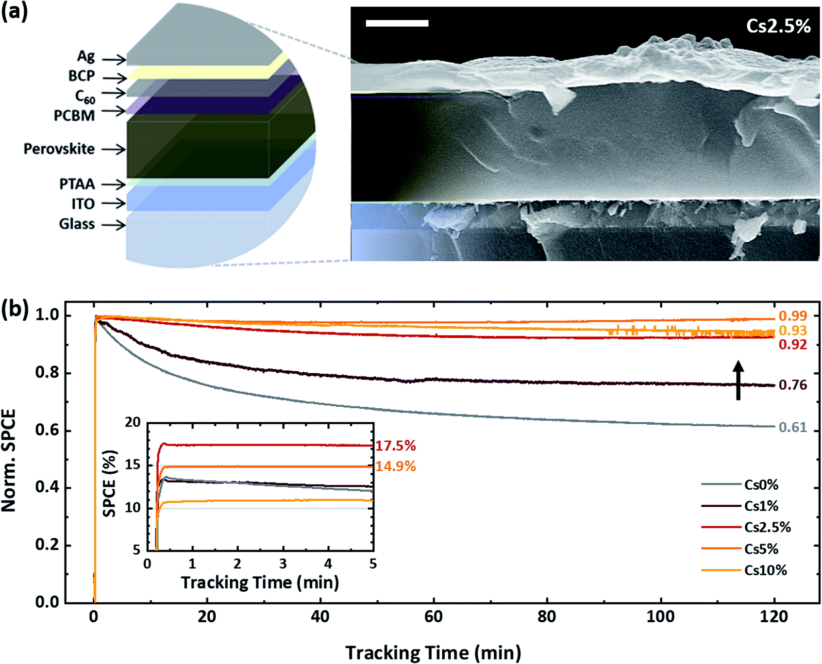 | ||
| Fig. 1 (a) Schematic illustration and a cross-sectional scanning electron microscopy (SEM) image of a low-bandgap (LBG) perovskite solar cell (PSC) composed of a triple-cation Csx(FA0.8MA0.2)(1−x)Sn0.5Pb0.5I3 LBG perovskite absorber layer with x = 2.5% (denoted as Cs2.5%). The scalebar on the top-left is indicative of 300 nm. (b) Stabilized power conversion efficiency (SPCE) of the best performing Csx(FA0.8MA0.2)(1−x)Sn0.5Pb0.5I3 LBG PSCs with different Cs concentrations varying from x = 0%, to 1%, 2.5%, 5%, and 10% (denoted as Cs0%, Cs1%, Cs2.5%, Cs5%, and Cs10%, respectively) under AM 1.5G illumination (100 mW cm−2) at MPP tracking conditions at 25 °C for 120 min; SPCE are normalized to their initial values (when the light is switched on). Inset: absolute values of the initial SPCE for the same PSCs over the first 5 min. | ||
To understand the role of Cs in the photovoltaic enhancement of the PSCs, we study the morphology and photo-physics of the perovskite thin-films in the following. SEM images (Fig. 2a) reveal that the perovskite thin-films with Cs0% to Cs5% are all compact and pinhole-free. In contrast, perovskite thin-films with Cs10% exhibit pinholes and cracks between the grains denoting a poor morphology with inhomogeneous coverage, which results in reduced photovoltaic performance in the respective PSCs (Fig. S3†). We also note that the size of the perovskite grains enlarges by increasing Cs concentration (from 217 nm for Cs0% to 570 nm for Cs10%), which is indicative of fewer grain boundaries, and therefore limited non-radiative recombination due to fewer trap states at the grain boundaries.56 Grain boundaries might result in increased recombination losses and decreased device stability under illumination due to defect-induced ion migration.57–59 Furthermore, SEM images exhibit the formation of bright nanosized aggregates (<100 nm) on the surface of LBG perovskite thin-films. These aggregates are mitigated by adding Cs and completely disappear by increasing the Cs concentration to 10% (Fig. 2a). The approximate relative area (RA) of the bright nanosized aggregates is compared with the stability factor (SF) and the average PCE (PCEave) of the PSCs as a function of Cs concentration in Fig. 2b. For the investigated range, there seems to be an optimal amount of Cs (2.5%) to obtain the highest PCEs, while a higher Cs concentration (5%) is beneficial for device photo-stability. Residual PbI2 is reported to cause degradation of the established Pb-based perovskite thin-films under illumination even in an inert atmosphere.60–63 Therefore, having verified that incorporating Cs decreases the aggregates observed on the surface of LBG perovskite thin-films and improves the operational photo-stability of the respective PSCs (Fig. 2b), one may hypothesize that these nanosized aggregates are residual PbI2 crystals that suffer from an intrinsic photo-instability caused by photo-decomposition under illumination.60,61,64,65 However, considering the chemical structure of our LBG perovskite, containing Sn and Pb, the bright nanosized aggregates might be also composed of residual SnI2 or SnyPb(1−y)I2. CL is a suitable characterization technique to detect phase segregations and residual materials such as PbI2 excess in perovskite thin-films.66–69 We compare CL spectra of LBG perovskite thin-films with different Cs concentrations within the spectral range from 400 to 900 nm (Fig. 3a). A broad CL peak located at around 600 nm gradually diminishes with increasing the concentration of Cs from 0% to 10%. This peak indicates the presence of a WBG phase or a material with a bandgap of about 2.1 eV, which is much higher than the bulk bandgap of LBG perovskite thin-films (∼1.26 eV). For comparison, we show CL spectra of pure PbI2, pure SnI2, mixed Sn0.5Pb0.5I2 thin-films. As presented in Fig. 3b, PbI2 and SnI2 thin-films exhibit narrow CL peaks at 505 and 518 nm, respectively. In contrast, the Sn0.5Pb0.5I2 thin-film exhibits a broad CL peak located at around 618 nm, which matches well with the CL emission peak around 600 nm determined for LBG perovskite thin-films. It should be noted that the trend observed for the bandgap of SnyPb(1−y)I2 (for y = 0, 0.5, and 1), which does not comply with Vegard's law, is similar to the trend reported for the bandgap of MASnxPb(1−x)I3 thin-films4 and is attributed to the “band inversion” in the literature.70,71 In conclusion, the CL suggest that the nanosized aggregates identified in the SEM images are mixed SnyPb(1−y)I2 composites with 0 < y < 1, the amount of which decreases with increasing the amount of Cs.
 | ||
| Fig. 2 (a) Top-view scanning electron microscopy (SEM) images of Csx(FA0.8MA0.2)(1−x)Sn0.5Pb0.5I3 low-bandgap perovskite thin-films with Cs concentrations varying from x = 0%, to 1%, 2.5%, 5%, and 10% (denoted as Cs0%, Cs1%, Cs2.5%, Cs5%, and Cs10%, respectively) deposited by the vacuum-assisted growth control method. The scalebar is indicative of 1 μm. (b) Comparison of the relative area (RA) of the bright nanosized aggregates (=area of the aggregates/area of the grains), the stability factor (SF = SPCEfinal/SPCEinitial), and the average PCE (PCEave) of the PSC devices, as a function of Cs content. SPCEfinal and SPCEinitial are the initial (when the light is switched on) and final (after 120 min) values of the SPCE derived from maximum power point (MPP) tracking under constant AM 1.5G solar illumination at 25 °C. | ||
 | ||
| Fig. 3 Cathodoluminescence (CL) spectra of a (a) Csx(FA0.8MA0.2)(1−x)Sn0.5Pb0.5I3 low-bandgap perovskite thin-films prepared by different Cs concentrations varying from x = 0%, to 1%, 2.5%, 5%, and 10% (denoted as Cs0%, Cs1%, Cs2.5%, Cs5%, and Cs10%, respectively), and (b) PbI2, SnI2, and Sn0.5Pb0.5I2 thin-films. | ||
To provide more insights into the role of Cs in decreasing the amount of these nanosized aggregates, as well as its effect on the crystallinity of LBG perovskite thin-films, we perform XRD measurements on perovskite thin-films with different Cs concentrations. The characteristic XRD peak of the underlying ITO substrate thin-film serves as a reference to precisely calibrate the XRD diffraction patterns. The XRD pattern of the perovskite thin-films with and without Cs exhibit two dominant perovskite peaks at 14.1° and 28.3° (Fig. 4a), which are assigned to the (002)/(110) and (004)/(220) planes of the tetragonal perovskite crystal-structure, respectively.12 We note that by increasing the Cs concentration from 0% to 5%, the intensity of these two characteristic peaks gradually increases, denoting a gradual change in the crystal orientation and/or the crystallinity of the perovskite thin-films. By contrast, perovskite thin-film with Cs10% exhibits the lowest XRD perovskite peak intensities, possibly caused by approaching the substitution limit (spinodal decomposition)46,72,73 and/or too high excess of cations in the perovskite precursor solution.63,64 Therefore, according to the XRD and SEM findings, incorporating Cs up to 5% leads to an enhanced crystallinity and/or preferential crystal orientation that correlates well with the gradual increase in the grains' sizes and the enhanced photovoltaic performance of the devices. We also notice a slight shift of the perovskite peaks to higher diffraction angles by increasing the concentration of Cs from 0% to 10% (Fig. S5a†).This shift indicates that Cs is incorporated into the perovskite lattice resulting in a lattice contraction since the ionic radius of Cs+ (1.81 Å) is much smaller than FA+ (2.79 Å) and MA+ (2.70 Å).38,46 The incorporation of Cs into the perovskite lattice is also confirmed by X-ray photo electron spectroscopy (XPS) presented in Fig. S5b.† The incorporation of Cs into the Sn–Pb-based perovskite material is reported to reduce the crystallization rate and effectively slows down the oxidation of Sn2+ to Sn4+, possibly as a result of lattice contraction and denser morphology of the perovskite thin-films.38 Most importantly, the XRD data manifest that as the concentration of Cs increases, the intensity of the small peak detected at 12.77° abates until it completely disappears for Cs10% (Fig. 4a, inset). XRD results derived from pure PbI2, pure SnI2, and Sn0.5Pb0.5I2 thin-films exhibit peaks at 12.65°, 12.76°, and 12.67°, respectively (Fig. S6†). While the signal quality of the XRD data of the perovskite thin-films (Fig. 4a) does not easily allow us to discriminate between these materials, by considering both XRD and CL results, we assign this peak to mixed SnyPb(1−y)I2 (0 < y < 1) that shrinks gradually upon adding more Cs, in line with the decreased amount of nanosized aggregates as observed with SEM. Given that these aggregates are located on the surface of LBG perovskite thin-films and have a bandgap of about 2.1 eV (as detected by CL), they could potentially mitigate the extraction of electrons from the perovskite thin-film to the PCBM ETL, and therefore reduce the operational photo-stability of the PSCs under constant illumination, as previously shown in Fig. 1b.
 | ||
| Fig. 4 X-ray diffraction (XRD) patterns of (a) Csx(FA0.8MA0.2)(1−x)Sn0.5Pb0.5I3 low-bandgap perovskite thin-films with different Cs concentrations varying from x = 0%, to 1%, 2.5%, 5%, and 10% (denoted as Cs0%, Cs1%, Cs2.5%, Cs5%, and Cs10%, respectively); inset exhibits suppression of the XRD peak at 12.77° by increasing Cs content. (b) Csx(FA0.8MA0.2)(1−x)Sn0.5Pb0.5I3 prepared with a varying excess of Sn and Pb (ySn0.5Pb0.5I2) from y = 7.5%, to 4.5% and 0% depending on the Cs concentrations which varies from x = 0%, to 3%, 7.5%, and 12.5%. | ||
To shed more light on the effectiveness of Cs in the diminution of residual SnyPb(1−y)I2, we carry out further XRD analyses on Csx(FA0.8MA0.2)(1−x)Sn0.5Pb0.5I3 thin-films that we intentionally prepared with prominent 7.5% of Sn and Pb excess, and varied the Cs concentration from x = 0% to 3%, 7.5%, and 12.5% (Fig. 4b). In the absence of Cs, there is a dominant peak at around 12.77° (in agreement with the small XRD peak detected for the LBG perovskite thin-films prepared without excess Sn and Pb (Fig. S4a†)) that is ascribed to the existence of large amount of residual SnyPb(1−y)I2. This peak significantly abates by adding only a minute amount of Cs (x = 3%), whereas the two main perovskite peaks detected at 14.1° and 28.3° are strongly intensified. Further increasing the amount of Cs results in further decrease (x = 7.5%) and complete disappearance (x = 12.5%) of the SnyPb(1−y)I2 XRD peak, with the perovskite peaks starting to exhibit a decrease at the same time. Ultraviolet-visible (UV-vis) spectroscopy of the samples (Fig. S7a†) exhibit that the absorption of the thin-films with x = 3% and 7.5% increases, whereas it significantly drops for x = 12.5%, in line with the average thickness of the thin-films, which are 490, 516, 534, and 300 nm for x = 0%, 3.5%, 7.5% and 12.5%, respectively (Fig. S7c†). The reduced absorption and layer thickness for a too large Cs concentration might be related to a substitution limit (spinodal decomposition)46,72,73 and/or too high excess of cations in the precursor solution,63,64 as discussed above. Since the bandgap of the thin-films with x = 3% and 7.5% is not altered by the amount of Cs content as evidenced in Fig. S7b,† an increase in their absorption can be indicative of a volumetric growth of the perovskite material, which agrees with the enhanced perovskite XRD peaks (Fig. 4b). These observations are also in line with the improved JSC of the PSCs with sufficient Cs concentrations (Fig. S3c†). Finally, another possible explanation for the reduction of the nanosized aggregates could be that the reaction between residual SnyPb(1−y)I2 and CsI results in a perovskite with a new composition. To corroborate this hypothesis, we investigate the XRD patterns of Cs1Sn0.5Pb0.5I3 thin-films, and find that the typical perovskite peaks appear at around 14.5° and 29.1° (Fig. S8†). This attests that incorporating Cs in LBG FA0.8MA0.2Sn0.5Pb0.5I3 with residual SnyPb(1−y)I2 in principle might also form a new Cs1Sn0.5Pb0.5I3 perovskite phase. However, the volume fraction of Cs1Sn0.5Pb0.5I3, if existed, must be very low, and therefore it would be hard to detect its XRD peaks in the XRD patterns of LBG perovskite thin-films shown in Fig. 4a. In summary, our observations reveal that there is an excess of Sn and Pb in the form of SnyPb(1−y)I2 (0 < y < 1) on the surface of FA0.8MA0.2Sn0.5Pb0.5I3 LBG perovskite thin-films that diminishes by only adding minute amounts of Cs. Reaction between residual SnyPb(1−y)I2 and Cs results in a volumetric growth of the LBG perovskite thin-films and leads to an enhanced crystallinity. This results in remarkably improved photo-stability of the respective PSCs.
Lastly, combining the LBG PSCs with Cs2.5% (Eg = 1.26 eV) with semi-transparent PSCs (Eg = 1.65 eV), we fabricate 4T all-PTSCs, as schematically illustrated in Fig. 5a. The semi-transparent PSC composed of a 2D/3D perovskite heterostructure has a regular configuration of glass/ITO/SnO2 nanoparticles (np-SnO2)/Cs0.17FA0.83Pb(I0.76Br0.24)3/2,2′,7,7′-tetrakis[N,N-di(4-methoxyphenyl)amino]-9,9′-spirobifluorene (spiro-MeOTAD)/molybdenum oxide (MoOx)/ITO/magnesium fluoride (MgF2).8 MoOx (10 nm) is to protect the spiro-MeOTAD layer against ion bombardment during the subsequent ITO sputtering process.74,75 In addition, an MgF2 thin-film (165 nm) on the sputtered ITO acts as an anti-reflection to increase the optical transmittance.76 The UV-vis absorbance spectra and the Tauc plots of the perovskite absorber layers applied for the semi-transparent top and the LBG bottom PSCs are presented in Fig. S9.† The best performing semi-transparent PSC and LBG PSC with Cs2.5% attain PCEs of 18.0% and 18.2%, respectively. Applying a semi-transparent perovskite filter (substrate area 225 mm2), which is fabricated under the same conditions and has the same structure as the semi-transparent PSCs, on top of the LBG PSCs, a PCE of 5.6% is attainable. By adding the PCE of the semi-transparent top PSC (=18.0%) and the PCE of the filtered LBG bottom PSC (=5.6%), we determine the efficiency of the corresponding 4T all-PTSC to be 23.6%. Fig. S10a and b† exhibit the transmittance (T), reflectance (R), and absorptance (A) spectra of a semi-transparent filter and an LBG perovskite thin-film with Cs2.5% deposited on PTAA-coated ITO, respectively. In addition, we compare the UV-vis spectra of the semi-transparent filters and semi-transparent PSCs (Fig. S11,† shown only for one filter and one cell) and observe an insignificant difference. The calculated JSC values from the integration of EQE spectra (Fig. 5c) are 19.5, 31.4, and 9.6 mA cm−2 for the semi-transparent top, stand-alone LBG bottom, and filtered LBG bottom PSCs, respectively. Table 1 summarizes the photovoltaic parameters for the champion top and bottom PSCs, as well as the calculated PCE of the corresponding 4T all-PTSCs. Similarly, we achieve promising results for the SPCEs (Fig. 5d). The semi-transparent top PSC provides a SPCE of 17.5%, whereas the bottom PSC has a SPCE of 17.5% (stand-alone) and 5.5% (filtered) from the MPP tracking under constant AM 1.5G illumination at 25 °C. Thereby, the corresponding 4T all-PTSC provides a SPCE of 23.0% by adding the SPCE values of the semi-transparent top PSC (=17.5%) and the filtered LBG bottom PSC (=5.5%). Furthermore, using a polydimethylsiloxane (PDMS) anti-reflection foil with a randomly inverted pyramid texture at the front-side of the semi-transparent PSC leads to a boost in the JSC by 1 mA cm−2 (compare J–V scans of the semi-transparent top PSC provided in Fig. 5b and S12a†). The PDMS foils are used to reduce the front-surface reflection losses.77–80 The textured PDMS foil we use here significantly reduces the reflectance from the glass ITO substrates (Fig. S13†). Therefore, by applying the PDMS foil, a single-junction semi-transparent PSC with a PCE and a SPCE as high as 18.9% and 18.3% is achievable (Fig. S12†). Applying the PDMS foil on the semi-transparent filter improves the PCE of the filtered LBG bottom PSC to 6.5%. Thereby, the PCE of the respective 4T all-PTSC is enhanced to 25.4%, if using a PDMS foil while measuring the sub-PSCs (Fig. S12 and Table S2†). Our results demonstrate the potential of the Cs-incorporated LBG perovskite thin-films in configuring high-efficiency 4T all-PTSCs with improved operational photo-stability. Future research should consider the potential improvement in the efficiency and the stability of the Cs-incorporated LBG PSCs through established methods such as incorporating antioxidant additives, applying 2D components as passivation layers, and introducing alternative cations into the perovskite lattice structure such as rubidium and potassium.
 | ||
| Fig. 5 (a) Schematic cross-sectional image of a 4T all-perovskite tandem solar cell (4T all-PTSC) configuration, implementing a semi-transparent top PSC (Eg = 1.65 eV) and a low-bandgap (LBG) bottom PSC (1.26 eV). (b) Current-density–voltage (J–V) scans measured at a fixed rate of 0.6 V s−1, from the open-circuit voltage (VOC) to the short-circuit current (JSC), (c) the external quantum efficiency (EQE), and (d) maximum power point (MPP) tracking measurements, of the semi-transparent top PSC and the LBG bottom PSC (stand-alone and filtered) under AM 1.5G illumination (100 mW cm−2) at 25 °C. PCE4T and SPCE4T are the calculated PCE and stabilized PCE derived from the J–V scans and the MPP tracking measurements for the champion 4T all-PTSC, respectively. The calculated JSC values from the EQE responses for the semi-transparent top, stand-alone LBG bottom, and filtered LBG bottom PSCs are 19.5, 31.4, and 9.6 mA cm−2, respectively. | ||
| Perovskite solar cell (PSC) | Scan direction | V OC (V) | J SC (mA cm−2) | FF (%) | PCE (%) | SPCE (%) |
|---|---|---|---|---|---|---|
| Semi-transparent top PSC | Backward | 1.16 | 19.7 | 78.7 | 18.0 | 17.5 |
| Forward | 1.13 | 20.0 | 74.8 | 16.9 | ||
| LBG bottom PSC (stand-alone) | Backward | 0.78 | 32.5 | 71.8 | 18.2 | 17.5 |
| Forward | 0.77 | 32.5 | 66.5 | 16.7 | ||
| LBG bottom PSC (filtered) | Backward | 0.76 | 10.2 | 72.2 | 5.6 | 5.5 |
| Forward | 0.75 | 10.2 | 68.4 | 5.2 | ||
| 4T all-PTSC | Backward | 23.6 | 23.0 | |||
| Forward | 22.1 |
3. Conclusion
In summary, we demonstrate that incorporating only minute quantities of Cs in double-cation Sn–Pb-based perovskite thin-films effectively improves the operational photo-stability of the low-bandgap PSCs. The Csx(FA0.8MA0.2)(1−x)Sn0.5Pb0.5I3 low-bandgap PSCs with x = 2.5% attain remarkable PCE as high as 18.2%. More importantly, perovskite solar cells prepared with x = 2.5% and 5% respectively maintain 92% and 99% of their initial PCE after 120 min of the MPP tracking under constant AM 1.5G solar illumination. Our observations demonstrate that the introduction of small quantities of Cs considerably reduces the formation of residual nanosized SnyPb(1−y)I2 (with 0 < y < 1) aggregates on the surface of the LBG perovskite thin-films, which is attributed to the reaction of Cs with the residual SnyPb(1−y)I2 and results in a volumetric growth of the perovskite thin-films. Furthermore, a beneficial stoichiometric composition and better crystallinity of the perovskite absorber is demonstrated for a sufficient amount of Cs that leads to an improvement in the photo-stability of the respective PSCs. Applying the low-bandgap PSCs together with semi-transparent top PSCs, we attain a 4T all-perovskite tandem solar cell with a PCE of 23.6% and a stabilized PCE of 23.0%, which are among the highest values reported to date in the literature.4. Experimental section
4.1. Preparation of perovskite precursor solution
For the triple-cation LBG perovskite precursor solution with the stoichiometric formula of Csx(FA0.8MA0.2)(1−x)Sn0.5Pb0.5I3, we first prepared the double-cation FA0.8MA0.2Sn0.5Pb0.5I3 perovskite precursor solution by dissolving 1.1 M formamidinium iodide (FAI, Dyesol), 0.3 M methylammonium iodide (MAI, Dyesol), 0.7 M tin iodide (SnI2, Alfa Aesar, 99.999%), 0.7 M lead iodide (PbI2, Alfa Aesar, 99.999%), 0.008 M lead thiocyanate (Pb(SCN)2, Sigma Aldrich, 99.5%), and 0.045 M tin fluoride (SnF2, Sigma Aldrich, 99%) in a 9:1 (v/v) mixture of dimethylformamide (DMF, Sigma Aldrich, anhydrous, 99.8%) and dimethyl sulfoxide (DMSO, Sigma Aldrich, anhydrous, ≥99.9%). Next, we prepared the cesium iodide (CsI, Alpha Aesar) stock solution by dissolving 1.5 M CsI in DMSO. By adding 8.8, 21.8, 42.4, and 80.4 μl of the 1.5 M CsI stock into 1 ml of the double-cation FA0.8MA0.2Sn0.5Pb0.5I3 perovskite precursor solution, we prepared the final triple-cation Csx(FA0.8MA0.2)(1−x)Sn0.5Pb0.5I3 perovskite solution for x = 0.01, 0.025, 0.05, and 0.1, respectively. After preparation, the solution was stored for 1 hour before fabrication in an N2-filled glovebox (O2 < 0.2 ppm and H2O < 0.4 ppm). For the Csx(FA0.8MA0.2)(1−x)Sn0.5Pb0.5I3 perovskite thin-films with Sn and Pb excess, we added additional PbI2 and SnI2 to FA0.8MA0.2Sn0.5Pb0.5I3 in order to achieve the required 7.5% excess Sn0.5Pb0.5I2, followed by adding Cs from a 1.5 M stock solution to reach 3%, 7.5%, and 12.5% Cs concentrations. For the double-cation perovskite precursor solution with the stoichiometric formula of Cs0.17FA0.83Pb(I0.76Br0.24)3, we mixed 0.83 mmol FAI, 0.17 mmol CsI, 0.64 mmol PbI2, and 0.36 mmol PbBr2 in a 4:1 (v/v) mixture of DMF:DMSO.
4.2. Solar cell fabrication
We fabricated the triple-cation LBG PSCs with an active area of 10.5 mm2 and a layer sequence of glass/indium tin oxide (ITO)/poly[bis(4-phenyl)(2,4,6-trimethylphenyl)amine] (PTAA)/Csx(FA0.8MA0.2)(1−x)Sn0.5Pb0.5I3/phenyl-C61-butyric acid methyl ester (PCBM)/buckminsterfullerene (C60)/2,9-dimethyl-4,7-diphenyl-1,10-phenanthroline (BCP)/silver (Ag). Initially, we cleaned the 16 × 16 mm2 glass substrates coated with 120 nm thick ITO layers (sheet resistance 15 Ω sq−1, Luminescence Technology) in an ultrasonic bath with acetone and isopropanol for 10 min each followed by an oxygen plasma treatment at 100 W power for 3 min. We spin-coated the glass ITO substrates with a ∼5 nm thin-film of PTAA (Mw = 17800 g mol−1, EM INDEX), as the hole transport layer at 4000 rpm for 30 s, followed by annealing at 100 °C for 30 min. Next, we deposited the LBG perovskite thin-film on the PTAA-coated substrates at 5000 rpm for 10 s. We immediately vacuum-exposed the layers for 10 s in a vacuum chamber (∼10 Pa) with a 150 ml volume size. We, sequentially, annealed the perovskite thin-films at 100 °C for 7 min. Next, we spin-coated the perovskite thin-film by a ∼5 nm thin-film of PCBM (Sigma Aldrich, 99.5%), which was prepared by dissolving 5 mg PCBM in 1 ml 1,2-dichlorobenzene (Sigma Aldrich, anhydrous, 99%) and spin-coated at 4000 rpm for 60 s. In sequence, we used a Lesker PVD system to thermally evaporate ∼20 nm of C60 (Sigma Aldrich, 99.5%) and ∼5 nm of BCP (Luminescence Technology) as the electron transport material, in 6 × 10⁻⁶ mbar pressure and at a rate of 0.1–0.2 and 0.2–0.3 Å s−1, respectively. We completed the PSC stack by evaporating a back contact of Ag (∼100 nm).
To fabricate the transparent double-cation PSCs with the same active area (10.5 mm2) and a layer sequence of ITO/SnO2 nanoparticles/Cs0.17FA0.83Pb(I0.76Br0.24)3/2,2′,7,7′-tetrakis[N,N-di(4-methoxyphenyl)amino]-9,9′-spirobifluorene (spiro-MeOTAD)/molybdenum oxide (MoOx)/ITO/magnesium fluoride (MgF2), we used sputtered ITO thin-films applying a Kurt J Lesker PVD-75 thin-film deposition system. The following sputtering parameters were used for the front (rear) ITO: power = 50 W (50 W), substrate temperature = 300 °C (25 °C), deposition time = 2000 s (2300 s), pressure = 0.8 mTorr (0.8 mTorr), O2 partial pressure = 3.5% (2.5%), and thickness ∼135 nm (150 nm). The sheet resistance of the sputtered ITO was 10–12 Ω sq−1 (40–50 Ω sq−1). First, we spin-coated the precleaned ITO substrates with SnO2 nanoparticles (Alfa Aesar, diluted in distilled water to a concentration of 2.04%) at 4000 rpm for 30 s, followed by a 250 °C annealing step for 30 min in an ambient atmosphere. Next, we deposited the double-cation perovskite absorber layer from solution by a two-step spin coating process: (i) 1000 rpm for 10 s, (ii) 5000 rpm for 30 s, while10 s before the end of the second step 100 μl chlorobenzene was poured on the spinning substrate. Annealing the samples at 100 °C for 30 min in an inert atmosphere was next. After the annealing step, we processed the 2D/3D perovskite heterostructure by spin-coating 100 μl n-butylammonium bromide (BABr, Dysol) dissolved in isopropanol (2 mg ml−1) at 5000 rpm for 30 s on top of the perovskite thin-film with subsequent annealing at 100 °C for 5 min in an inert atmosphere. Next, we deposited spiro-MeOTAD as the hole transport layer using a spin-coating process with 4000 rpm for 30 s. A 10 nm thin-film of MoOx (Sigma Aldrich) was thermally evaporated on spiro-MeOTAD using a Lesker PVD system at a rate of 0.8 Å s−1 and in 6 × 10⁻⁶ mbar pressure. To increase the conductivity of the rear ITO, we thermal-evaporated ∼75 nm Au fingers at a rate of 2 Å s−1 using a shadow mask. We completed the stack by depositing ∼165 nm MgF2 as an anti-reflection layer on top of the rear ITO using a Lesker PVD system at a rate of 3–4 Å s−1 and in 6 × 10⁻⁶ mbar pressure.
4.3. Characterization
Conflicts of interest
There are no conflicts to declare.Acknowledgements
We acknowledge support by the KIT-Publication Fund of the Karlsruhe Institute of Technology. We would like to thank Dirk Hauschild (KIT) and Lothar Weinhardt (KIT) for XPS measurements. S. M. would like to acknowledge the financial support from DAAD (Deutscher Akademischer Austauschdienst/German academic exchange service) for her doctoral research work under personal reference number 91621525. The financial support by Alexander von Humboldt (Georg Forster Research Fellowship), German Federal Ministry of Education and Research (BMBF) through PRINTPERO (03SF0557A) project, German Federal Ministry for Economic Affairs and Energy (CAPITANO, funding code: 03EE1038B), the Initiating and Networking funding of Helmholtz Association HYIG of U.W.P. (VH-NG-1148), Helmholtz Energy Materials Foundry (HEMF), PEROSEED (ZT-0024), Science and Technology of Nanostructures (STN), and Karlsruhe School of Optics & Photonics (KSOP) is gratefully acknowledged. T. D. acknowledges the financial support of a Postdoc Fellowship from the Australian Centre for Advanced Photovoltaics (ACAP). Part of the experiment was performed at the Australian National Fabrication Facility (ANFF) ACT Node.References
- A. Kojima, K. Teshima, Y. Shirai and T. Miyasaka, J. Am. Chem. Soc., 2009, 131, 6050–6051 CAS.
- https://www.nrel.gov/pv/assets/pdfs/best-research-cell-efficiencies.20200128.pdf, accessed 25 September 2020.
- W. Shockley and H. J. Queisser, J. Appl. Phys., 1961, 32, 510–519 CAS.
- F. Hao, C. C. Stoumpos, R. P. H. Chang and M. G. Kanatzidis, J. Am. Chem. Soc., 2014, 136, 8094–8099 CrossRef CAS.
- J. Im, C. C. Stoumpos, H. Jin, A. J. Freeman and M. G. Kanatzidis, J. Phys. Chem. Lett., 2015, 6, 3503–3509 CrossRef CAS.
- J. H. Noh, S. H. Im, J. H. Heo, T. N. Mandal and S. Il Seok, Nano Lett., 2013, 13, 1764–1769 CrossRef CAS.
- X. Zhang, J. Liu, Z. Song, W. Zuo, Z. Fan, X. He, K. Luo, Q. Ye and C. Liao, Phys. Status Solidi, 2019, 216, 1800727 CrossRef.
- S. Gharibzadeh, I. M. Hossain, P. Fassl, B. A. Nejand, T. Abzieher, M. Schultes, E. Ahlswede, P. Jackson, M. Powalla, S. Schäfer, M. Rienäcker, T. Wietler, R. Peibst, U. Lemmer, B. S. Richards and U. W. Paetzold, Adv. Funct. Mater., 2020, 30, 1909919 CrossRef CAS.
- D. P. McMeekin, G. Sadoughi, W. Rehman, G. E. Eperon, M. Saliba, M. T. Horantner, A. Haghighirad, N. Sakai, L. Korte, B. Rech, M. B. Johnston, L. M. Herz and H. J. Snaith, Science, 2016, 351, 151–155 CrossRef CAS.
- S. Gharibzadeh, B. Abdollahi Nejand, M. Jakoby, T. Abzieher, D. Hauschild, S. Moghadamzadeh, J. A. Schwenzer, P. Brenner, R. Schmager, A. A. Haghighirad, L. Weinhardt, U. Lemmer, B. S. Richards, I. A. Howard and U. W. Paetzold, Adv. Energy Mater., 2019, 9, 1803699 CrossRef.
- D. Zhao, C. Wang, Z. Song, Y. Yu, C. Chen, X. Zhao, K. Zhu and Y. Yan, ACS Energy Lett, 2018, 3, 305–306 CrossRef CAS.
- D. Zhao, Y. Yu, C. Wang, W. Liao, N. Shrestha, C. R. Grice, A. J. Cimaroli, L. Guan, R. J. Ellingson, K. Zhu, X. Zhao, R.-G. Xiong and Y. Yan, Nat. Energy, 2017, 2, 17018 CrossRef CAS.
- G. E. Eperon, T. Leijtens, K. A. Bush, R. Prasanna, T. Green, J. T. W. Wang, D. P. McMeekin, G. Volonakis, R. L. Milot, R. May, A. Palmstrom, D. J. Slotcavage, R. A. Belisle, J. B. Patel, E. S. Parrott, R. J. Sutton, W. Ma, F. Moghadam, B. Conings, A. Babayigit, H. G. Boyen, S. Bent, F. Giustino, L. M. Herz, M. B. Johnston, M. D. McGehee and H. J. Snaith, Science, 2016, 354, 861–865 CrossRef CAS.
- T. Leijtens, R. Prasanna, K. A. Bush, G. E. Eperon, J. A. Raiford, A. Gold-Parker, E. J. Wolf, S. A. Swifter, C. C. Boyd, H.-P. Wang, M. F. Toney, S. F. Bent and M. D. McGehee, Sustain. Energy Fuels, 2018, 2, 2450–2459 RSC.
- M. Anaya, J. P. Correa-Baena, G. Lozano, M. Saliba, P. Anguita, B. Roose, A. Abate, U. Steiner, M. Grätzel, M. E. Calvo, A. Hagfeldt and H. Míguez, J. Mater. Chem. A, 2016, 4, 11214–11221 RSC.
- B. Abdollahi Nejand, I. M. Hossain, M. Jakoby, S. Moghadamzadeh, T. Abzieher, S. Gharibzadeh, J. A. Schwenzer, P. Nazari, F. Schackmar, D. Hauschild, L. Weinhardt, U. Lemmer, B. S. Richards, I. A. Howard and U. W. Paetzold, Adv. Energy Mater., 2020, 10, 1902583 CrossRef CAS.
- J. Tong, Z. Song, D. H. Kim, X. Chen, C. Chen, A. F. Palmstrom, P. F. Ndione, M. O. Reese, S. P. Dunfield, O. G. Reid, J. Liu, F. Zhang, S. P. Harvey, Z. Li, S. T. Christensen, G. Teeter, D. Zhao, M. M. Al-Jassim, M. F. A. M. van Hest, M. C. Beard, S. E. Shaheen, J. J. Berry, Y. Yan and K. Zhu, Science, 2019, 364, 475–479 CrossRef CAS.
- R. Lin, K. Xiao, Z. Qin, Q. Han, C. Zhang, M. Wei, M. I. Saidaminov, Y. Gao, J. Xu, M. Xiao, A. Li, J. Zhu, E. H. Sargent and H. Tan, Nat. Energy, 2019, 4, 864–873 CrossRef CAS.
- S. Ternes, T. Börnhorst, J. A. Schwenzer, I. M. Hossain, T. Abzieher, W. Mehlmann, U. Lemmer, P. Scharfer, W. Schabel, B. S. Richards and U. W. Paetzold, Adv. Energy Mater., 2019, 9, 1901581 CrossRef CAS.
- T. Abzieher, J. A. Schwenzer, S. Moghadamzadeh, F. Sutterluti, I. M. Hossain, M. Pfau, E. Lotter, M. Hetterich, B. S. Richards, U. Lemmer, M. Powalla and U. W. Paetzold, IEEE J. Photovoltaics, 2019, 9, 1249–1257 Search PubMed.
- T. Abzieher, S. Moghadamzadeh, F. Schackmar, H. Eggers, F. Sutterlüti, A. Farooq, D. Kojda, K. Habicht, R. Schmager, A. Mertens, R. Azmi, L. Klohr, J. A. Schwenzer, M. Hetterich, U. Lemmer, B. S. Richards, M. Powalla and U. W. Paetzold, Adv. Energy Mater., 2019, 9, 1802995 CrossRef.
- B. Zhao, M. Abdi-Jalebi, M. Tabachnyk, H. Glass, V. S. Kamboj, W. Nie, A. J. Pearson, Y. Puttisong, K. C. Gödel, H. E. Beere, D. A. Ritchie, A. D. Mohite, S. E. Dutton, R. H. Friend and A. Sadhanala, Adv. Mater., 2017, 29, 1604744 CrossRef.
- W. Liao, D. Zhao, Y. Yu, N. Shrestha, K. Ghimire, C. R. Grice, C. Wang, Y. Xiao, A. J. Cimaroli, R. J. Ellingson, N. J. Podraza, K. Zhu, R.-G. Xiong and Y. Yan, J. Am. Chem. Soc., 2016, 138, 12360–12363 CrossRef CAS.
- E. S. Parrott, T. Green, R. L. Milot, M. B. Johnston, H. J. Snaith and L. M. Herz, Adv. Funct. Mater., 2018, 28, 1802803 CrossRef.
- T. Leijtens, R. Prasanna, A. Gold-Parker, M. F. Toney and M. D. McGehee, ACS Energy Lett, 2017, 2, 2159–2165 CrossRef CAS.
- Z. Shi, J. Guo, Y. Chen, Q. Li, Y. Pan, H. Zhang, Y. Xia and W. Huang, Adv. Mater., 2017, 29, 1605005 CrossRef.
- K. P. Marshall, M. Walker, R. I. Walton and R. A. Hatton, Nat. Energy, 2016, 1, 16178 CrossRef CAS.
- M. H. Kumar, S. Dharani, W. L. Leong, P. P. Boix, R. R. Prabhakar, T. Baikie, C. Shi, H. Ding, R. Ramesh, M. Asta, M. Graetzel, S. G. Mhaisalkar and N. Mathews, Adv. Mater., 2014, 26, 7122–7127 CrossRef CAS.
- T. M. Koh, T. Krishnamoorthy, N. Yantara, C. Shi, W. L. Leong, P. P. Boix, A. C. Grimsdale, S. G. Mhaisalkar and N. Mathews, J. Mater. Chem. A, 2015, 3, 14996–15000 RSC.
- S. Gupta, D. Cahen and G. Hodes, J. Phys. Chem. C, 2018, 122, 13926–13936 CrossRef CAS.
- M. C. Jung, S. R. Raga and Y. Qi, RSC Adv., 2016, 6, 2819–2825 RSC.
- C.-M. Tsai, H.-P. Wu, S.-T. Chang, C.-F. Huang, C.-H. Wang, S. Narra, Y.-W. Yang, C.-L. Wang, C.-H. Hung and E. W.-G. Diau, ACS Energy Lett, 2016, 1, 1086–1093 CrossRef CAS.
- X. Xu, C.-C. Chueh, Z. Yang, A. Rajagopal, J. Xu, S. B. Jo and A. K. Y. Jen, Nano Energy, 2017, 34, 392–398 CrossRef CAS.
- Q. Tai, X. Guo, G. Tang, P. You, T. W. Ng, D. Shen, J. Cao, C. K. Liu, N. Wang, Y. Zhu, C. S. Lee and F. Yan, Angew. Chemie - Int. Ed., 2019, 58, 806–810 CrossRef CAS.
- M. Wei, K. Xiao, G. Walters, R. Lin, Y. Zhao, M. I. Saidaminov, P. Todorović, A. Johnston, Z. Huang, H. Chen, A. Li, J. Zhu, Z. Yang, Y. Wang, A. H. Proppe, S. O. Kelley, Y. Hou, O. Voznyy, H. Tan and E. H. Sargent, Adv. Mater., 2020, 32, 1907058 CrossRef CAS.
- Z. Chen, M. Liu, Z. Li, T. Shi, Y. Yang, H.-L. Yip and Y. Cao, iScience, 2018, 9, 337–346 CrossRef CAS.
- E. Ruggeri, M. Anaya, K. Gałkowski, G. Delport, F. U. Kosasih, A. Abfalterer, S. Mackowski, C. Ducati and S. D. Stranks, Adv. Mater., 2019, 31, 1905247 CrossRef CAS.
- X. Liu, Z. Yang, C.-C. Chueh, A. Rajagopal, S. T. Williams, Y. Sun and A. K. Y. Jen, J. Mater. Chem. A, 2016, 4, 17939–17945 RSC.
- T. Jiang, Z. Chen, X. Chen, T. Liu, X. Chen, W. E. I. Sha, H. Zhu and Y. Yang, Sol. RRL, 2020, 4, 1900467 CrossRef CAS.
- E. J. Juarez-Perez, L. K. Ono and Y. Qi, J. Mater. Chem. A, 2019, 7, 16912–16919 RSC.
- E. J. Juarez-Perez, L. K. Ono, M. Maeda, Y. Jiang, Z. Hawash and Y. Qi, J. Mater. Chem. A, 2018, 6, 9604–9612 RSC.
- W. Nie, J.-C. Blancon, A. J. Neukirch, K. Appavoo, H. Tsai, M. Chhowalla, M. A. Alam, M. Y. Sfeir, C. Katan, J. Even, S. Tretiak, J. J. Crochet, G. Gupta and A. D. Mohite, Nat. Commun., 2016, 7, 11574 CrossRef CAS.
- F. Arabpour Roghabadi, M. Alidaei, S. M. Mousavi, T. Ashjari, A. S. Tehrani, V. Ahmadi and S. M. Sadrameli, J. Mater. Chem. A, 2019, 7, 5898–5933 RSC.
- C. C. Stoumpos, C. D. Malliakas and M. G. Kanatzidis, Inorg. Chem., 2013, 52, 9019–9038 CrossRef CAS.
- Z. Li, M. Yang, J.-S. Park, S.-H. Wei, J. J. Berry and K. Zhu, Chem. Mater., 2016, 28, 284–292 CrossRef CAS.
- M. Saliba, T. Matsui, J.-Y. Seo, K. Domanski, J.-P. Correa-Baena, M. K. Nazeeruddin, S. M. Zakeeruddin, W. Tress, A. Abate, A. Hagfeldt and M. Grätzel, Energy Environ. Sci., 2016, 9, 1989–1997 RSC.
- Y. Hu, E. M. Hutter, P. Rieder, I. Grill, J. Hanisch, M. F. Aygüler, A. G. Hufnagel, M. Handloser, T. Bein, A. Hartschuh, K. Tvingstedt, V. Dyakonov, A. Baumann, T. J. Savenije, M. L. Petrus and P. Docampo, Adv. Energy Mater., 2018, 8, 1703057 CrossRef.
- G. Kapil, T. Bessho, C. H. Ng, K. Hamada, M. Pandey, M. A. Kamarudin, D. Hirotani, T. Kinoshita, T. Minemoto, Q. Shen, T. Toyoda, T. N. Murakami, H. Segawa and S. Hayase, ACS Energy Lett, 2019, 4, 1991–1998 CrossRef CAS.
- C. Li, Z. Song, D. Zhao, C. Xiao, B. Subedi, N. Shrestha, M. M. Junda, C. Wang, C. S. Jiang, M. Al-Jassim, R. J. Ellingson, N. J. Podraza, K. Zhu and Y. Yan, Adv. Energy Mater., 2019, 9, 1803135 CrossRef.
- D. Zhao, C. Chen, C. Wang, M. M. Junda, Z. Song, C. R. Grice, Y. Yu, C. Li, B. Subedi, N. J. Podraza, X. Zhao, G. Fang, R. G. Xiong, K. Zhu and Y. Yan, Nat. Energy, 2018, 3, 1093–1100 CrossRef CAS.
- B. Roose, A. Ummadisingu, J.-P. Correa-Baena, M. Saliba, A. Hagfeldt, M. Graetzel, U. Steiner and A. Abate, Nano Energy, 2017, 39, 24–29 CrossRef CAS.
- N. Ito, M. A. Kamarudin, D. Hirotani, Y. Zhang, Q. Shen, Y. Ogomi, S. Iikubo, T. Minemoto, K. Yoshino and S. Hayase, J. Phys. Chem. Lett., 2018, 9, 1682–1688 CrossRef CAS.
- C. Fei and H. Wang, Org. Electron., 2019, 68, 143–150 CrossRef CAS.
- T. T. Ngo, E. M. Barea, R. Tena-Zaera and I. Mora-Seró, ACS Appl. Energy Mater., 2018, 1, 4057–4064 CrossRef CAS.
- S. Moghadamzadeh, I. M. Hossain, M. Jakoby, B. Abdollahi Nejand, D. Rueda-Delgado, J. A. Schwenzer, S. Gharibzadeh, T. Abzieher, M. R. Khan, A. A. Haghighirad, I. A. Howard, B. S. Richards, U. Lemmer and U. W. Paetzold, J. Mater. Chem. A, 2020, 8, 670–682 RSC.
- H. Do Kim, H. Ohkita, H. Benten and S. Ito, Adv. Mater., 2016, 28, 917–922 CrossRef.
- A. F. Castro-Méndez, J. Hidalgo and J. P. Correa-Baena, Adv. Energy Mater., 2019, 9, 1–10 Search PubMed.
- W. Chen, Y. Wang, G. Pang, C. W. Koh, A. B. Djurišić, Y. Wu, B. Tu, F. Liu, R. Chen, H. Y. Woo, X. Guo and Z. He, Adv. Funct. Mater., 2019, 29, 1808855 CrossRef.
- M. M. Tavakoli, M. Saliba, P. Yadav, P. Holzhey, A. Hagfeldt, S. M. Zakeeruddin and M. Grätzel, Adv. Energy Mater., 2019, 9, 1802646 CrossRef.
- J. Schoonman, Chem. Phys. Lett., 2015, 619, 193–195 CrossRef CAS.
- F. Liu, Q. Dong, M. K. Wong, A. B. Djurišić, A. Ng, Z. Ren, Q. Shen, C. Surya, W. K. Chan, J. Wang, A. M. C. Ng, C. Liao, H. Li, K. Shih, C. Wei, H. Su and J. Dai, Adv. Energy Mater., 2016, 6, 1502206 Search PubMed.
- Y. H. Lee, J. Luo, R. Humphry-Baker, P. Gao, M. Grätzel and M. K. Nazeeruddin, Adv. Funct. Mater., 2015, 25, 3925–3933 CrossRef CAS.
- T. J. Jacobsson, J.-P. Correa-Baena, E. Halvani Anaraki, B. Philippe, S. D. Stranks, M. E. F. Bouduban, W. Tress, K. Schenk, J. Teuscher, J.-E. Moser, H. Rensmo and A. Hagfeldt, J. Am. Chem. Soc., 2016, 138, 10331–10343 CrossRef CAS.
- P. Fassl, V. Lami, A. Bausch, Z. Wang, M. T. Klug, H. J. Snaith and Y. Vaynzof, Energy Environ. Sci., 2018, 11, 3380–3391 RSC.
- B. Roose, K. Dey, Y.-H. Chiang, R. H. Friend and S. D. Stranks, J. Phys. Chem. Lett., 2020, 11, 6505–6512 CrossRef CAS.
- T. Duong, H. Pham, T. C. Kho, P. Phang, K. C. Fong, D. Yan, Y. Yin, J. Peng, M. A. Mahmud, S. Gharibzadeh, B. A. Nejand, I. M. Hossain, M. R. Khan, N. Mozaffari, Y. Wu, H. Shen, J. Zheng, H. Mai, W. Liang, C. Samundsett, M. Stocks, K. McIntosh, G. G. Andersson, U. Lemmer, B. S. Richards, U. W. Paetzold, A. Ho-Ballie, Y. Liu, D. Macdonald, A. Blakers, J. Wong-Leung, T. White, K. Weber and K. Catchpole, Adv. Energy Mater., 2020, 10, 1903553 CrossRef CAS.
- C. Xiao, Z. Li, H. Guthrey, J. Moseley, Y. Yang, S. Wozny, H. Moutinho, B. To, J. J. Berry, B. Gorman, Y. Yan, K. Zhu and M. Al-Jassim, J. Phys. Chem. C, 2015, 119, 26904–26911 CrossRef CAS.
- T. Duong, H. K. Mulmudi, Y. Wu, X. Fu, H. Shen, J. Peng, N. Wu, H. T. Nguyen, D. Macdonald, M. Lockrey, T. P. White, K. Weber and K. Catchpole, ACS Appl. Mater. Interfaces, 2017, 9, 26859–26866 CrossRef CAS.
- T. Duong, H. K. Mulmudi, H. Shen, Y. L. Wu, C. Barugkin, Y. O. Mayon, H. T. Nguyen, D. Macdonald, J. Peng, M. Lockrey, W. Li, Y. B. Cheng, T. P. White, K. Weber and K. Catchpole, Nano Energy, 2016, 30, 330–340 CrossRef CAS.
- X. Gao and M. S. Daw, Phys. Rev. B, 2008, 77, 033103 CrossRef.
- J. O. Dimmock, I. Melngailis and A. J. Strauss, Phys. Rev. Lett., 1966, 16, 1193–1196 CrossRef CAS.
- R. G. Niemann, L. Gouda, J. Hu, S. Tirosh, R. Gottesman, P. J. Cameron and A. Zaban, J. Mater. Chem. A, 2016, 4, 17819–17827 RSC.
- F. Brivio, C. Caetano and A. Walsh, J. Phys. Chem. Lett., 2016, 7, 1083–1087 CrossRef CAS.
- D. Zhao, C. Zhang, H. Kim and L. J. Guo, Adv. Energy Mater., 2015, 5, 1500768 CrossRef.
- K. A. Bush, A. F. Palmstrom, Z. J. Yu, M. Boccard, R. Cheacharoen, J. P. Mailoa, D. P. McMeekin, R. L. Z. Hoye, C. D. Bailie, T. Leijtens, I. M. Peters, M. C. Minichetti, N. Rolston, R. Prasanna, S. Sofia, D. Harwood, W. Ma, F. Moghadam, H. J. Snaith, T. Buonassisi, Z. C. Holman, S. F. Bent and M. D. McGehee, Nat. Energy, 2017, 2, 17009 CrossRef CAS.
- Q. Han, Y.-T. Hsieh, L. Meng, J.-L. Wu, P. Sun, E.-P. Yao, S.-Y. Chang, S.-H. Bae, T. Kato, V. Bermudez and Y. Yang, Science, 2018, 361, 904–908 CrossRef CAS.
- S. Manzoor, Z. J. Yu, A. Ali, W. Ali, K. A. Bush, A. F. Palmstrom, S. F. Bent, M. D. McGehee and Z. C. Holman, Sol. Energy Mater. Sol. Cells, 2017, 173, 59–65 CrossRef CAS.
- S. Dottermusch, R. Schmager, E. Klampaftis, S. Paetel, O. Kiowski, K. Ding, B. S. Richards and U. W. Paetzold, Prog. Photovoltaics Res. Appl., 2019, 27, 3133 CrossRef.
- R. Schmager, B. Fritz, R. Hünig, K. Ding, U. Lemmer, B. S. Richards, G. Gomard and U. W. Paetzold, ACS Photonics, 2017, 4, 2687–2692 CrossRef CAS.
- M. Langenhorst, D. Ritzer, F. Kotz, P. Risch, S. Dottermusch, A. Roslizar, R. Schmager, B. S. Richards, B. E. Rapp and U. W. Paetzold, ACS Appl. Mater. Interfaces, 2019, 11, 35015–35022 CrossRef CAS.
- C. D. Wagner and G. E. Muilenberg, Handbook of X-ray photoelectron spectroscopy, Perkin-Elmer, 1979 Search PubMed.
Footnote |
| † Electronic supplementary information (ESI) available. See DOI: 10.1039/d0ta07005j |
| This journal is © The Royal Society of Chemistry 2020 |