
 Open Access Article
 This Open Access Article is licensed under a Creative Commons Attribution-Non Commercial 3.0 Unported Licence
Chemical vapor deposited polymer layer for efficient passivation of planar perovskite solar cells†
Mahdi
Malekshahi Byranvand‡
 ab,
Farid
Behboodi-Sadabad‡
*c,
Abed
Alrhman Eliwi
b,
Vanessa
Trouillet
de,
Alexander
Welle
ce,
Simon
Ternes
ab,
Ihteaz Muhaimeen
Hossain
ab,
Motiur Rahman
Khan
b,
Jonas Alexander
Schwenzer
b,
Amjad
Farooq
ab,
Bryce Sydney
Richards
ab,
Joerg
Lahann
*cf and
Ulrich Wilhelm
Paetzold
*ab
ab,
Farid
Behboodi-Sadabad‡
*c,
Abed
Alrhman Eliwi
b,
Vanessa
Trouillet
de,
Alexander
Welle
ce,
Simon
Ternes
ab,
Ihteaz Muhaimeen
Hossain
ab,
Motiur Rahman
Khan
b,
Jonas Alexander
Schwenzer
b,
Amjad
Farooq
ab,
Bryce Sydney
Richards
ab,
Joerg
Lahann
*cf and
Ulrich Wilhelm
Paetzold
*ab
aInstitute of Microstructure Technology, Karlsruhe Institute of Technology, Hermann-von-Helmholtz-Platz 1, 76344 Eggenstein-Leopoldshafen, Germany. E-mail: ulrich.paetzold@kit.edu
bLight Technology Institute, Karlsruhe Institute of Technology, Engesserstrasse 13, 76131 Karlsruhe, Germany
cInstitute of Functional Interfaces, Karlsruhe Institute of Technology, Hermann-von-Helmholtz-Platz 1, 76344 Eggenstein-Leopoldshafen, Germany. E-mail: farid.sadabad@kit.edu; joerg.lahann@kit.edu
dInstitute for Applied Materials, Karlsruhe Institute of Technology, 76344 Eggenstein-Leopoldshafen, Germany
eKarlsruhe Nano Micro Facility, Karlsruhe Institute of Technology, 76344 Eggenstein-Leopoldshafen, Germany
fBiointerfaces Institute, Departments of Chemical Engineering, Materials Science and Engineering, Macromolecular Science and Engineering and Biomedical Engineering, University of Michigan, Ann Arbor, Michigan 48109, USA
First published on 18th September 2020
Abstract
Reducing non-radiative recombination losses by advanced passivation strategies is pivotal to maximize the power conversion efficiency (PCE) of perovskite solar cells (PSCs). Previously, polymers such as poly(methyl methacrylate), poly(ethylene oxide), and polystyrene were successfully applied in solution-processed passivation layers. However, controlling the thickness and homogeneity of these ultra-thin passivation layers on top of polycrystalline perovskite thin films is a major challenge. In response to this challenge, this work reports on chemical vapor deposition (CVD) polymerization of poly(p-xylylene) (PPX) layers at controlled substrate temperatures (14–16 °C) for efficient surface passivation of perovskite thin films. Prototype double-cation PSCs using a ∼1 nm PPX passivation layer exhibit an increase in open-circuit voltage (VOC) of ∼40 mV along with an enhanced fill factor (FF) compared to a non-passivated PSC. These improvements result in a substantially enhanced PCE of 20.4% compared to 19.4% for the non-passivated PSC. Moreover, the power output measurements over 30 days under ambient atmosphere (relative humidity ∼40–50%) confirm that the passivated PSCs are more resilient towards humidity-induced degradation. Considering the urge to develop reliable, scalable and homogeneous deposition techniques for future large-area perovskite solar modules, this work establishes CVD polymerization as a novel approach for the passivation of perovskite thin films.
Introduction
Organic–inorganic perovskite materials have drawn tremendous attention for optoelectronic devices over the past decade, given their exceptional optoelectronic properties and use of low-cost precursor materials.1–4 By compositional engineering,5,6 optimization of the perovskite thin film morphology,7–9 and interfacial passivation,10–13 the performance of perovskite photovoltaics was significantly improved, reaching power conversion efficiencies (PCEs) of single-junction perovskite solar cells (PSCs) exceeding 25% in 2019.14 This study engages with surface passivation, a strategy that is key to reduce the non-radiative recombination losses at the interface of the perovskite thin film and the electron transport layer (ETL) or hole transport layer (HTL), thereby reducing the dark saturation current and, in turn, enhancing the open circuit-voltage (VOC) and fill factor (FF) of PSCs.15,16 Moreover, interface passivation layers were reported to improve the stability of PSCs with regard to external stress caused by humidity,17–19 light20–22 and temperature.23,24In the conventional n–i–p PSC architecture, the bottom n-type ETL is commonly composed of a robust inorganic material such as TiO2 or SnO2 that exhibits a high tolerance toward surface treatments, enabling the facile application of passivation on top of these ETLs.25–28 In contrast, surface passivation of the interface between the perovskite and the p-type HTL is more challenging because of the sensitivity of perovskite thin films against surface treatments, such as polar solvents or post-processing heat treatment.29,30 Several materials such as metal oxides, small organic molecules and polymers have been explored in the past for passivation of the perovskite/HTL interface in PSCs of n–i–p architecture.31–33 In particular, insulating polymer layers processed from solution such as poly(methyl methacrylate) (PMMA),34,35 poly(ethylene oxide) (PEO),17 polystyrene36,37 and poly(4-vinylpyridine) (PVP)38 were successfully applied to suppress interfacial recombination losses, leading to enhanced VOC and FF. However, controlling the thickness and ensuring conformal coating of the polycrystalline perovskite thin film by solution-processed polymer layers imposes some critical challenges. Firstly, the thicknesses must be in the order of only a few nanometers to avoid large series resistances while maintaining good surface coverage to ensure sufficient passivation.34,39 Secondly, considering that the surfaces of solution-processed perovskite thin films are rough – a typical root mean square roughness (rms) is ∼30 nm – the deposition of homogeneous polymer layers becomes very difficult by solution-processing techniques.31,36 For these reasons, it is of key interest to develop a solvent-free deposition technique that enables the formation of a polymer passivation layer on rough textures of the perovskite films with precisely controlled thickness. Chemical vapor deposition (CVD) polymerization is able to deposit polymer coatings over large surface areas and has been used widely to fabricate consumer products.40–42 Besides the main advantage of being solvent-, plasticizer- and initiator-free, which ensures high purity in the large-area deposition, CVD polymerization allows for a precise thickness control of the polymer layer.43,44 Additionally, CVD typically results in pinhole-free layers and conformal coating of nanometer sized features.41,42 CVD polymerization can be operated at low temperatures (∼14–16 °C), which is beneficial for preventing temperature induced degradation of the perovskite thin films.45,46 Furthermore, CVD polymerization provides well-defined linear polymer coatings due to its well-defined reaction pathway and low propensity for chemical side reactions.41,47 These features, combined with the fact that passivation layers created by CVD polymerization are intrinsically compatible with flexible perovskite solar cells, may offset the potentially higher processing costs due to the need for vacuum-based processing. Previously, the one-step CVD polymerization technique was used to form functional coatings48 and nanofibers40 on a variety of substrates49 based on the Gorham process.47 Recently, CVD polymerization was used for encapsulation of PSCs in order to slow down the decomposition reactions of perovskite in high humidity atmosphere.50
This work reports on CVD polymerization as a technique for the finely-controlled deposition of homogeneous poly(p-xylylene) (PPX) polymer passivation layers onto the surface of perovskite thin films. By carefully optimizing the thickness of the PPX layers incorporated in double-cation PSCs, non-radiative recombination at the perovskite/HTL interface is efficiently suppressed, yielding high PCE solar cells with negligible hysteresis. The formation of the ultra-thin PPX layers and their effect on the optoelectronic properties of perovskite thin films are investigated by means of X-ray photoelectron spectroscopy (XPS), time-of-flight secondary-ion mass spectrometry (ToF-SIMS), and photoluminescence (PL) spectroscopy. Furthermore, the present work demonstrates that the moisture stability of the passivated PSC compared to a non-passivated one under ambient humidity is significantly improved.
Results and discussion
Ultra-thin PPX layers of thicknesses between 0.5 nm and 5 nm are deposited on the surface of the double-cation perovskite thin films via the CVD polymerization of [2.2]paracyclophane monomer (Fig. 1a and b). During the CVD polymerization process, the monomer sublimes at elevated temperatures (90–120 °C) and later forms radicals during the pyrolysis step at 660 °C, while flowing through a 320 mm long quartz tube with the argon (Ar) carrier gas. Finally, the polymerization occurs on top of the cooled perovskite thin film substrates (14–16 °C) in the polymerization chamber that is equipped with a rotatable sample holder (Scheme S1†). This cooled substrate prevents perovskite thin films degradation during the passivation process, which encourages future work on flexible perovskite thin film passivation. The thickness of the PPX layers deposited on the surface of perovskite thin films is determined by ellipsometry. These measurements indicate the deposition of homogenous PPX layers with the thickness of 0.5 ± 0.2, 1.0 ± 0.2, 2.0 ± 0.3, and 5.0 ± 0.3 nm on the surface of the perovskite thin films (Table S1†). During PPX deposition, the thickness of the PPX layer increases linearly with the amount of monomer supplied (Fig. S1†). Therefore, the thickness of PPX layer can be controlled by feeding a precise amount of monomer into the sublimation zone of the CVD setup. SEM images of the cross section of silicon wafers coated with a PPX layer with thickness of 10 nm, 25 nm, and 50 nm are shown in Fig. S2.†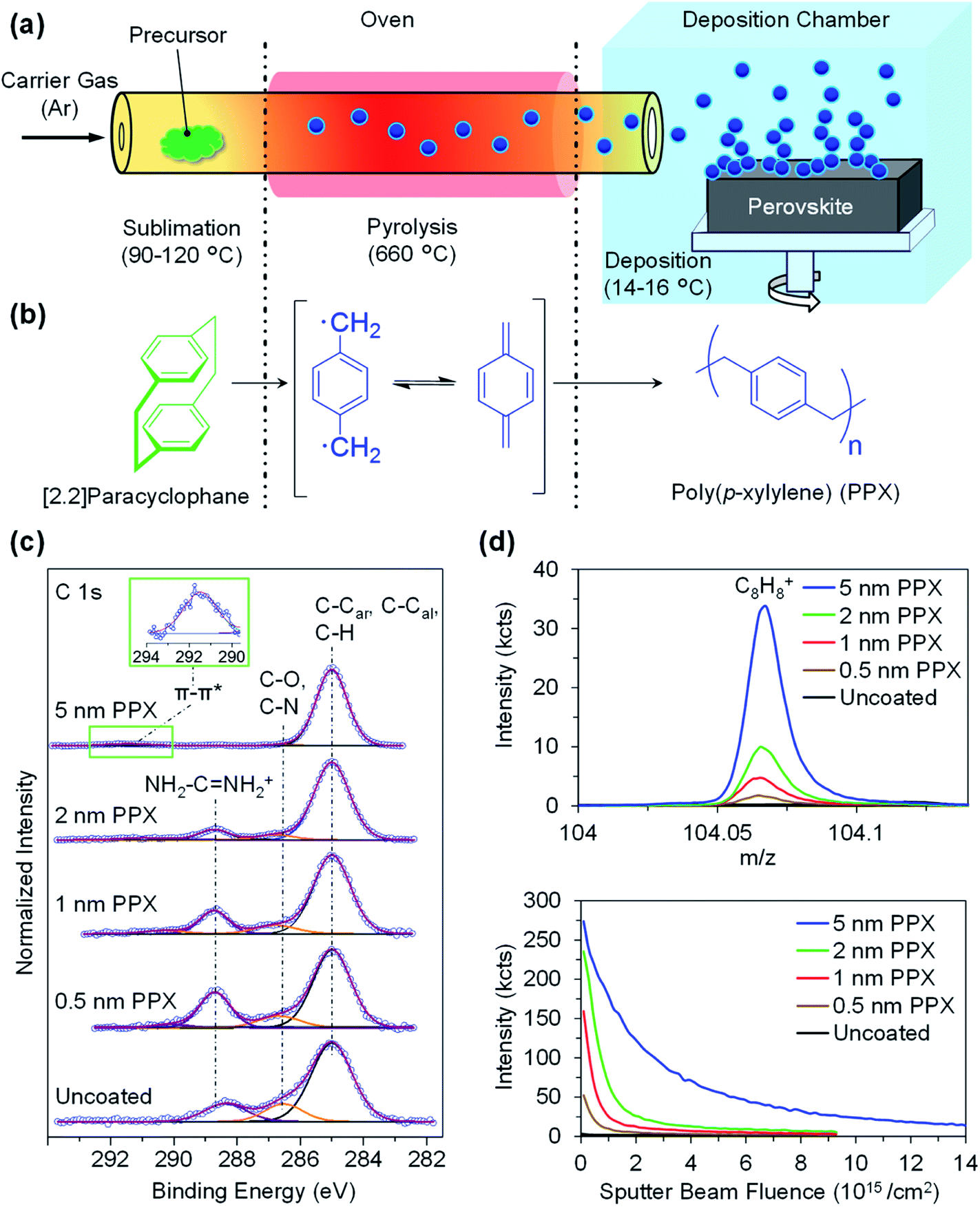 | ||
| Fig. 1 (a) Schematic illustration of the CVD polymerization process: polymer precursor sublimation, radicalization and the deposition of a PPX ultra-thin layer on top of perovskite thin film. (b) Chemical structures for the different steps of polymerization. (c) Detailed XPS C 1s spectra of uncoated perovskite, 0.5 nm, 1 nm, 2 nm, and 5 nm PPX-coated perovskite thin films indicates an increase of the C–C, C–H contribution after deposition of the PPX layer. For the 5 nm PPX layer, at ∼291.5 eV the weak π–π* transition signal (characteristic for PPX) appeared. For a better visualization, all spectra are normalized to the maximum of intensity. (d) ToF-SIMS data: depth integrated signals of the C8H8+ secondary ion (a representative fragment for the repeating unit of PPX) (top). Depth profiles of uncoated perovskite (black), and perovskite after deposition of 0.5 nm (brown), 1 nm (red), 2 nm (green), and 5 nm (blue) PPX on the surface obtained by Ar1200, 2.5 keV erosion. | ||
In order to prove the presence of the PPX layers and analyse the surface chemistry of PPX-coated perovskite thin films, XPS and ToF-SIMS measurements on uncoated and coated perovskite thin films with PPX layer thickness of 0.5 nm, 1 nm, 2 nm, and 5 nm are conducted. The C 1s XP spectra of the uncoated, 0.5 nm, 1 nm, 2 nm and 5 nm PPX-coated perovskites are depicted in Fig. 1c. The spectrum of the uncoated perovskite shows three components at 285.0 eV (C–C, C–H), at 286.5 eV (C–N) and at 288.5 eV (NH2–C![[double bond, length as m-dash]](https://www.rsc.org/images/entities/char_e001.gif) NH2+) stemming from a carbon contamination layer and from components of the perovskite layer (formamidinium and methylammonium). Along with the deposition of the PPX layer, an increase in the intensity of the aliphatic and aromatic component at 285.0 eV is observed in comparison to the contributions stemming from the perovskite thin film. Deposition of the PPX layer can be quantitatively monitored by the increase of various ratios, namely here the ratio (C–C, C–H)/(C–N) from 4.2 for uncoated perovskite to 6.0, 8.6, 20.1 and 63.4 for 0.5 nm, 1 nm, 2 nm, and 5 nm PPX-coated perovskites respectively (Table 1), proving the formation of a carbon-rich layer. Because of the information depth of XPS, comparable results are obtained for the 0.5 nm layer and the uncoated sample with its usually observed contamination. Moreover, the typically weak peak corresponding to the π–π* transition at ∼291.5 eV (characteristic for PPX containing aromatic rings) appears for the 5 nm PPX-coated perovskite (Fig. 1c inset). In correspondence with the increased PPX contributions, the concentration of iodine (characteristic for the perovskite) decreases from 41.5 at% for uncoated perovskite down to 7.7 at% along the thickness series studied (Table 1) and similarly, the concentration of Pb (further characteristic signal for the perovskite) decreases clearly from 15.3 at% for uncoated perovskite thin film down to 2.8 at% for 5 nm PPX-coated perovskite thin films. The drop in the intensity of both characteristic signals of perovskite (Pb and I) reveals the presence of a further layer on the surface. This can be demonstrated in addition by the evolution of the ratio between (C–C, C–H) moieties to I (and Pb) (Table 1). Overall, the increase of the signals stemming from PPX and attenuation of the signals from perovskite confirm the deposition of the PPX on the surface of the perovskite thin film.
NH2+) stemming from a carbon contamination layer and from components of the perovskite layer (formamidinium and methylammonium). Along with the deposition of the PPX layer, an increase in the intensity of the aliphatic and aromatic component at 285.0 eV is observed in comparison to the contributions stemming from the perovskite thin film. Deposition of the PPX layer can be quantitatively monitored by the increase of various ratios, namely here the ratio (C–C, C–H)/(C–N) from 4.2 for uncoated perovskite to 6.0, 8.6, 20.1 and 63.4 for 0.5 nm, 1 nm, 2 nm, and 5 nm PPX-coated perovskites respectively (Table 1), proving the formation of a carbon-rich layer. Because of the information depth of XPS, comparable results are obtained for the 0.5 nm layer and the uncoated sample with its usually observed contamination. Moreover, the typically weak peak corresponding to the π–π* transition at ∼291.5 eV (characteristic for PPX containing aromatic rings) appears for the 5 nm PPX-coated perovskite (Fig. 1c inset). In correspondence with the increased PPX contributions, the concentration of iodine (characteristic for the perovskite) decreases from 41.5 at% for uncoated perovskite down to 7.7 at% along the thickness series studied (Table 1) and similarly, the concentration of Pb (further characteristic signal for the perovskite) decreases clearly from 15.3 at% for uncoated perovskite thin film down to 2.8 at% for 5 nm PPX-coated perovskite thin films. The drop in the intensity of both characteristic signals of perovskite (Pb and I) reveals the presence of a further layer on the surface. This can be demonstrated in addition by the evolution of the ratio between (C–C, C–H) moieties to I (and Pb) (Table 1). Overall, the increase of the signals stemming from PPX and attenuation of the signals from perovskite confirm the deposition of the PPX on the surface of the perovskite thin film.
| I (at%) | Pb (at%) | (C–C, C–H)/I | (C–C, C–H)/Pb | (C–C, C–H)/(C–N) | |
|---|---|---|---|---|---|
| Uncoated | 41.5 | 15.3 | 0.5 | 1.5 | 4.2 |
| 0.5 nm PPX | 41.3 | 13.9 | 0.5 | 1.6 | 6.0 |
| 1 nm PPX | 36.5 | 12.2 | 0.8 | 2.4 | 8.6 |
| 2 nm PPX | 27.2 | 9.3 | 1.7 | 4.8 | 20.1 |
| 5 nm PPX | 7.7 | 2.8 | 9.9 | 25.3 | 63.4 |
These observations are further supported by ToF-SIMS depth profiles. For this purpose, dual beam depth profiles were recorded using Bi3+, 25 keV, primary ions during a low energy argon ion cluster (Ar1200, 2.5 keV) bombardment until the lead signals stabilized and the PPX signals (C8H8+ and other hydrocarbons) dropped to <5% of their initial value. The depth integrated signals of the C8H8+, a characteristic mass fragment for the repeating unit of the PPX polymer layer, increase significantly for the 1 nm, 2 nm, and the 5 nm PPX-coated perovskite thin film (Fig. 1d top). The relative intensities of the C8H8+ signals are proportional to the thicknesses of the PPX layers deposited on the surface of the perovskite thin films as determined by ellipsometry (Fig. S3†). Furthermore, depth profiles of C8H8+ measured on uncoated and PPX-coated perovskite thin films, shown in Fig. 1d bottom, are in good agreement with the amounts expected for the deposited PPX layers. Altogether, ellipsometry, XPS, and ToF-SIMS analyses of PPX-coated perovskite thin films strongly indicate that the PPX layers with thicknesses of 0.5–5 nm are successfully deposited on the perovskite surface by CVD polymerization. We further observed that the polymer films deposited by CVD, but not the corresponding precursor, are stable against common solvents such as ethanol and acetone (Fig. S4†). The polymeric nature of the PPX layer on a silicon wafer (after washing with ethanol and acetone) was confirmed by XPS and ToF-SIMS (Fig. S4a and b†). As a next step, it is confirmed that the ultra-thin PPX layer does not alter the morphology and crystallinity of the underlying perovskite thin films. Scanning electron microscopy (SEM) images of uncoated and coated perovskite thin films with 1 nm and 5 nm thick PPX layers exhibit the same surface morphology (Fig. S5a–c†). Moreover, the same characteristic X-ray diffraction (XRD) peaks before and after CVD polymerization are observed for the perovskite thin films, which indicates that the crystallinity of perovskite does not alter by the PPX deposition (Fig. S5d†). Given that the deposited PPX layers are ultra-thin, the absorbance of the perovskite thin films is not affected (Fig. S5e†). Therefore, the parasitic absorption losses caused by the PPX deposition are negligible.
To evaluate the effect of the ultra-thin PPX layers on the underlying perovskite thin films, the performance of PSCs incorporating these layers is investigated. To this end, the PSCs are fabricated using the following planar n–i–p PSC architecture: glass substrate, indium tin oxide (ITO) front electrode, nanoparticle-based SnO2 ETL, double-cation perovskite ((FAPbI3)0.97(MAPbBr3)0.03) thin film, 2,2′,7,7-tetrakis(N,N′-di-p-methoxy phenylamine)-9,9-spirobifluorene (spiro-OMeTAD) HTL and gold back electrode (ESI†).51,52 The PPX layers are deposited with varying thicknesses (0.5, 1, 2 and 5 nm) on top of the perovskite thin films. Cross-sectional SEM images of the PSCs show the respective layer stacks (Fig. S6†). Fig. 2a–d shows the statistical data of photovoltaic parameters for both reverse and forward scan direction of the J–V characteristic of 25 PSCs that were passivated with a range of different thicknesses of PPX layers at the perovskite/HTL interface. It should be noted that the JSC of J–V measurements is updated by the calculated correction factor of the JSC derived from EQE, which will be discussed later. Both, the VOC and FF gradually increase up to an optimal thickness of the PPX layer around 1 nm and decrease for higher thicknesses in forward as well as reverse scan direction. This decrement with high PPX thicknesses is attributed to the insulating characteristic of the PPX layer, which impacts all relevant photovoltaic parameters at higher thicknesses and is accompanied by a significant increase in series resistance (RS) (see Fig. S7 and Table S2†). The advantage of the PPX as a passivation layer for the PSCs is highlighted by the increase in VOC peaking at a PPX thickness of 1 nm with an average value of 1.11 V, exceeding the VOC of the uncoated reference PSCs at 1.09 V. Moreover, as shown in Fig. 2a–d and S8,† PSCs with passivating PPX layers of optimized thickness, i.e. 1 nm, show low hysteresis, which we ascribe to the efficient suppression of charge accumulation at the perovskite/HTL interface of passivated perovskite thin film. The hysteresis for 5 nm PPX coated samples is significantly increased compared to the devices with lower PPX thicknesses as well as the reference, which is attributed to the fact that thick PPX layers act as insulators (Fig. S7 and Table S2†).
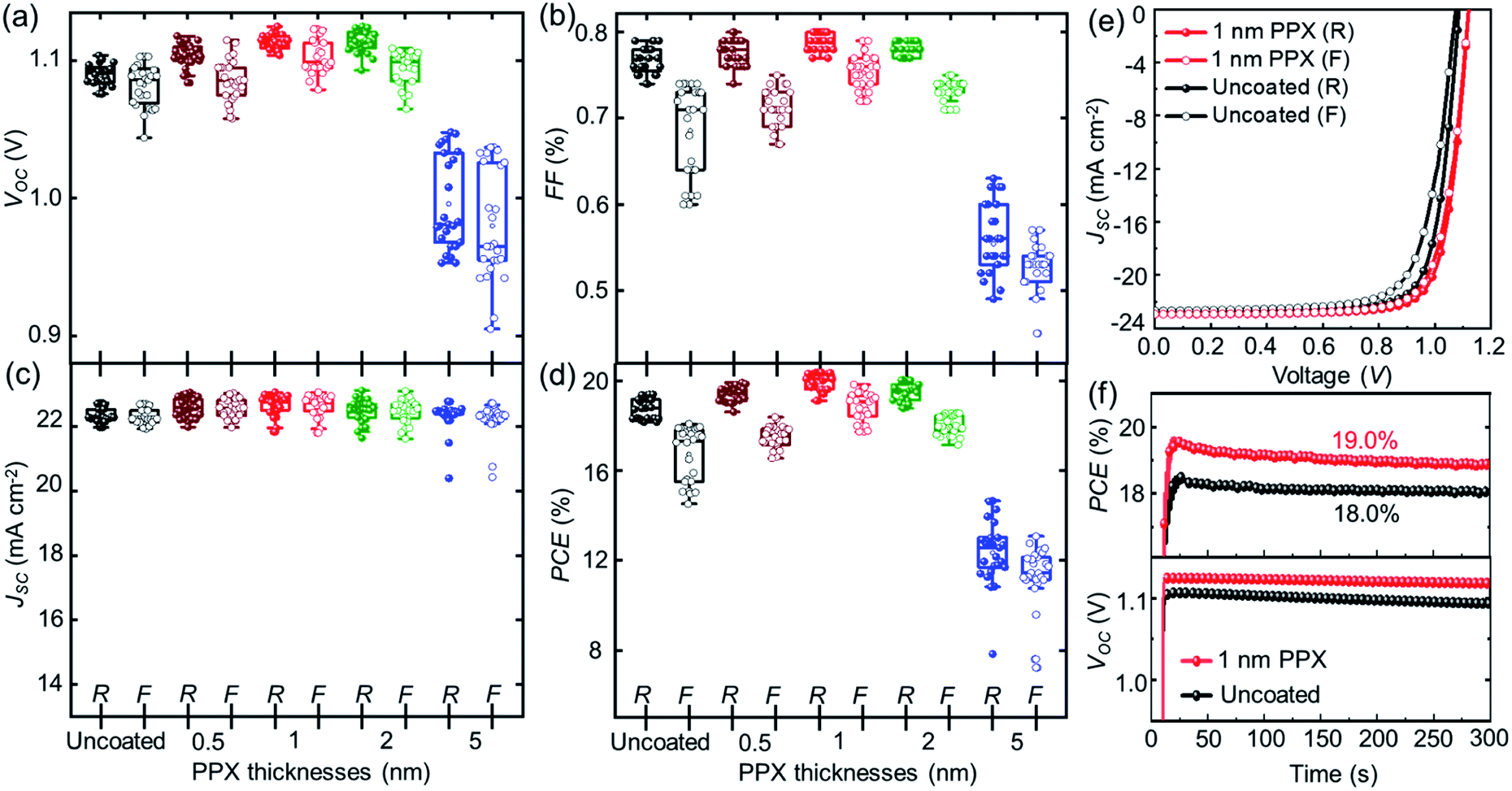 | ||
| Fig. 2 Photovoltaic parameters extracted from both reverse (closed symbols) and forward (open symbols) direction of J–V measurement of 25 PSCs fabricated with uncoated and different thicknesses of the PPX passivation layer coated perovskite thin films: (a) VOC, (b) FF, (c) JSC and (d) PCE. (e) The champion J–V characteristics with reverse and forward scans under standard test conditions (1000 W m−2 intensity, AM1.5G spectrum, and 25 °C device temperature). (f) Stabilized PCE (top) and VOC (bottom) during MPP tracking. | ||
A detailed analysis of the passivation properties of PPX layer follows in the subsequent section by means of photoluminescence spectroscopy. The PPX layer of 1 nm thickness provides combination of an efficient passivation and sufficient conductivity. The average PCE of fabricated PSCs with uncoated and 1 nm PPX-coated perovskite thin films increased from 18.4% up to 19.8%, evaluating 25 samples per category (Fig. S8†).
These results suggest that 1 nm is the optimum thickness of passivation layer on top of the perovskite thin film. Therefore, photovoltaic and optoelectronic properties of the 1 nm PPX-coated perovskite thin film are investigated in more detail.
Several reports show that the VOC can be significantly improved by means of solution-processed passivation layers. For example, our group recently demonstrated that by creating a very thin layer of two-dimensional (2D) perovskite at the interface of high band gap three-dimensional (3D) perovskite (≈1.72 eV) and HTL, the VOC has improved to 1.31 V with VOC deficit of 0.41 V.53 The PPX interlayer used in this work distinct from the 2D/3D perovskite hetero-structure, as it is deposited via a solvent-free CVD polymerization, allowing precise control over the thickness of the passivation layer and good homogeneity on large areas.
By keeping all the experimental conditions constant during the CVD process (i.e. operating temperatures and pressures) and feeding a precise amount of monomer in each run, uniform deposition of the PPX layer was achieved. To demonstrate the homogeneity on a macroscopic scale, up to 16 samples (perovskite thin film substrates) with the dimensions of 1.6 × 1.6 cm2 were coated (Scheme S2†). No relevant thickness variation was observed for the 16 samples that are placed 1 cm apart, showing that uniform deposition of PPX coatings on areas of up to 9.5 × 9.5 cm2 is feasible. Table S1† shows the film thickness, determined by ellipsometry measurements, for several spots on three random substrates per PPX deposition (targeted thickness of 0.5 nm, 1 nm, 2 nm and 5 nm). Exemplary, fitted parameters and the quality of the fit in the ellipsometry experiments for a 1 nm PPX layer are reported in Fig. S9.† It should be noted that we apply for convenience a Cauchy model that is suitable for transparent materials and therefore of limited relevance for wavelengths shorter than 370 nm (see Fig. S9†), where PPX layers exhibit some absorption.54 For each PPX deposition, the standard deviation in film thickness remains <0.2 nm (see Table S1†), highlighting the good homogeneity on a macroscopic-scale. In general, we expect also a high degree of conformality on a sub-micrometer scale for the PPX layer, since the monomer possesses very low values of sticking coefficients. However, characterization of the degree of conformality on a sub-micrometer scale in our system involves reporting of extensive data and analysis, which is out of scope of the current work. We also refer to our previous work, wherein we have demonstrated the ability to deposit the PPX polymer with controlled thickness on multiple samples on a large area of 15 cm in diameter.41,43
The very good homogeneity of the PPX layer becomes evident when comparing the four solar cells processed simultaneously on the same device. As shown in Fig. S10a,† the PSC with PPX layer exhibit almost identical J–V characteristics and photovoltaic parameters (Table S3†), strongly encouraging the conclusion that the passivation layer obtained in one CVD run is homogeneous over the whole area of the four cells. Furthermore, the reproducibility of the CVD passivation method is demonstrated by comparing the PCEs of 25 passivated PSCs per category from 4 batches. As shown in Fig. S10b,† PSCs of different batches show almost identical PCEs with an average of 19.8%, 19.9%, 19.7%, and 19.8% for run#1, run#2, run#3 and run#4, respectively. These results prove that PPX passivation of perovskite thin films by the CVD method is reproducible.
In Fig. 2e, the J–V characteristic of the champion PSC incorporates a 1 nm PPX-coated perovskite thin film (i.e. passivated PSC), corresponding to a very high PCE of 20.4% in reference to the champion PSC incorporating uncoated perovskite thin film (i.e., non-passivated PSC) exhibiting a PCE of 19.4%. The corresponding photovoltaic parameters are summarized in Table S4.† It should be noted that it is an ongoing challenge in the field of perovskite photovoltaics to ascertain an agreement between JSC derived from EQE and J–V characteristics.55,56 Also in this study, we observed a significant difference. However, as the absolute value of JSC is not key to this work and we prefer to be conservative in reporting PCE, we applied a mismatch factor to the JSC driven from J–V that accounts for the lower JSC derived from EQE (Fig. S11†). This factor is consequently applied to all measured J–V characteristics. The VOC and FF are significantly increased for the passivated PSC, which is attributed to the suppressed non-radiative recombination at the interface of HTL due to the incorporation of the PPX layer on top of the perovskite thin film. These improvements are in good agreement with previous reports on the passivation of perovskite thin films by other organic or inorganic layers. For instance, Matsudo's group and Miyasaka's group separately suggested that incorporating a solution-processed polymer layers of PMMA and PVP with thicknesses about 5–10 nm between the perovskite thin film and the HTL can reduce the surface trap states and non-radiative recombination as demonstrated by photoluminescence and impedance spectroscopy, which significantly improved the VOC, FF and PSC performance.38,39 Atomic layer deposition (ALD) is a successful example of a solvent-free method for the passivation of perovskite thin films. For example, Koushik and co-workers demonstrated that an ultra-thin (1–2 nm) Al2O3 passivation layer deposited by ALD on top of a perovskite thin film can effectively improve the VOC and FF in planar perovskite solar cells.31 While ALD is a layer-by-layer deposition process that is particularly suited for processing high quality inorganic passivation layers on top of perovskite thin films, this work reports on the solvent-free deposition of PPX polymer passivation layers deposited by CVD polymerization. CVD polymerization is a facile solvent-free deposition technique that allows maintaining low substrate temperatures (∼15 °C) and deposition of PPX passivation layers in a single process step. In addition, we want to point out that the PPX passivation layers deposited by CVD yield similar improvements in device performance compared to established solution-proceed polymers passivation layers such as PMMA.35 Fig. S12a–h† compares the improvement in device performance of PSCs with PMMA layers processed from a range of concentrations (0.2, 0.5, 1 mg ml−1) to the PPX passivation layers developed in this work. A comparable ΔVOC ∼ 0.04 mV and ΔFF ∼ 3% are shown with both passivation strategies. The highest improvement in ΔFF and ΔVOC are demonstrated for the PPX passivation layer of nominal thickness ∼1 nm. Therefore, our results encourage future work on alternative solvent-free deposition methods of polymer passivation layers such as molecular layer deposition. Furthermore, the decreased hysteresis for the passivated PSC is attributed to the efficient suppression of charge accumulation at the perovskite/HTL interface of passivated perovskite thin films as well as the passivation of defect at this interface. The stabilized PCE, determined by maximum power point (MPP) tracking of the PSCs under continuous illumination, is enhanced for the passivated PSC to 19% compared to 18% for the non-passivated PSC (Fig. 2f top). It should be noted that the passivated PSC shows higher and stable VOC for 300 s of constant illumination of one sun (Fig. 2f bottom). To acquire more reliable results regarding the performance stability, the MPP tracking of the PSCs is measured under continuous illumination for 60 min. As shown in Fig. S13,† the passivated and non-passivated PSCs show exquisite long-term PCE stability that is in good accordance with short-term MPP tracking (Fig. 2f top). Zhang and co-workers observed a similar improvement in MPP tracked PCE by inserting a solution-processed polystyrene layer at the interface of perovskite/HTL. They attributed this effect to reduced number of interface traps and defects, resulting in reduced non-radiative recombination.37
To rule out that the process conditions during the CVD polymerization (vacuum, substrate temperature etc.) affect the quality of the perovskite thin films, the performance of reference PSCs without PPX passivation is compared to PSCs that underwent the entire CVD deposition process without any precursor being supplied during the deposition step. As shown in Fig. S14,† the photovoltaic parameters are very similar for both cases, which confirms that the CVD polymerization process that encompasses vacuum and a low substrate temperature (14–16 °C) cannot be held responsible for the observed passivation of the PPX layers.
Next, the origin of the superior optoelectronic quality of the perovskite thin films passivated with a 1 nm PPX layer is explored by means of steady-state PL and time resolved photoluminescence (TRPL). For this purpose, the uncoated and 1 nm PPX-coated perovskite thin films are deposited on bare glass. As shown in Fig. 3a and b, the PPX layer approximately doubles the intensity of the steady state PL intensity and the charge carrier lifetime from 294 ns to around 419 ns. Both aspects highlight that the ultra-thin PPX layer strongly improves the optoelectronic quality of the perovskite thin film. Considering our previous observation that the PPX layer changes the chemical environment at the surface of the perovskite thin film and improves the PCE in PSCs, it is concluded that the PPX polymer passivates surface defects and trap states that are apparent for the double-cation perovskite thin film employed in this work.57 By passivating these defects, non-radiative recombination at the perovskite/HTL interface is suppressed, leading to an enhanced PL and a longer minority charge carrier lifetime. Furthermore, the ideality factor is determined from the VOC dependence on the light intensity in order to obtain indications on the relevant recombination mechanism at the perovskite/HTL interface in PSCs. The variation in ideality factor between 1 and 2 in PSCs is commonly interpreted in terms of the competition between radiative recombination (band to band), trap-assisted recombination in the bulk (SRH recombination), and surface recombination.58–60 The values of ideality factors for the non-passivated and the passivated PSCs are found to be 2.08 and 1.48, respectively (Fig. S15†). This is a further indication for suppression of trap-assisted SRH recombination by surface passivation, which is attributed to the reduced surface defects on the perovskite/HTL interface and is in good agreement with the PL data. For illustration, the suggested mechanism of the PPX passivation effect at the surface of the perovskite thin film is schematically presented in Fig. 3c and d. It is hypothesized that the grains and grain boundaries on the surface of perovskite thin films accommodate several defects or trap states such as cation vacancies and anti-site substitutional defects, as depicted in Fig. 3c.61 In the ideal device, the photogenerated charge carriers should reach the respective contact stacks without non-radiative recombination at either interface, i.e., the perovskite/HTL interface. Thin film characterizations and photovoltaic characterizations suggest that the ultra-thin PPX layer can passivate the defects and trap states and facilitate the hole transport at the interface of perovskite/HTL. Identifying the optimal balance between surface passivation and increased resistance of the PPX layer is key to obtain high final performance of the solar cells, which is again the focus of this work that introduces the CVD polymerization as a novel and powerful technique for this purpose.
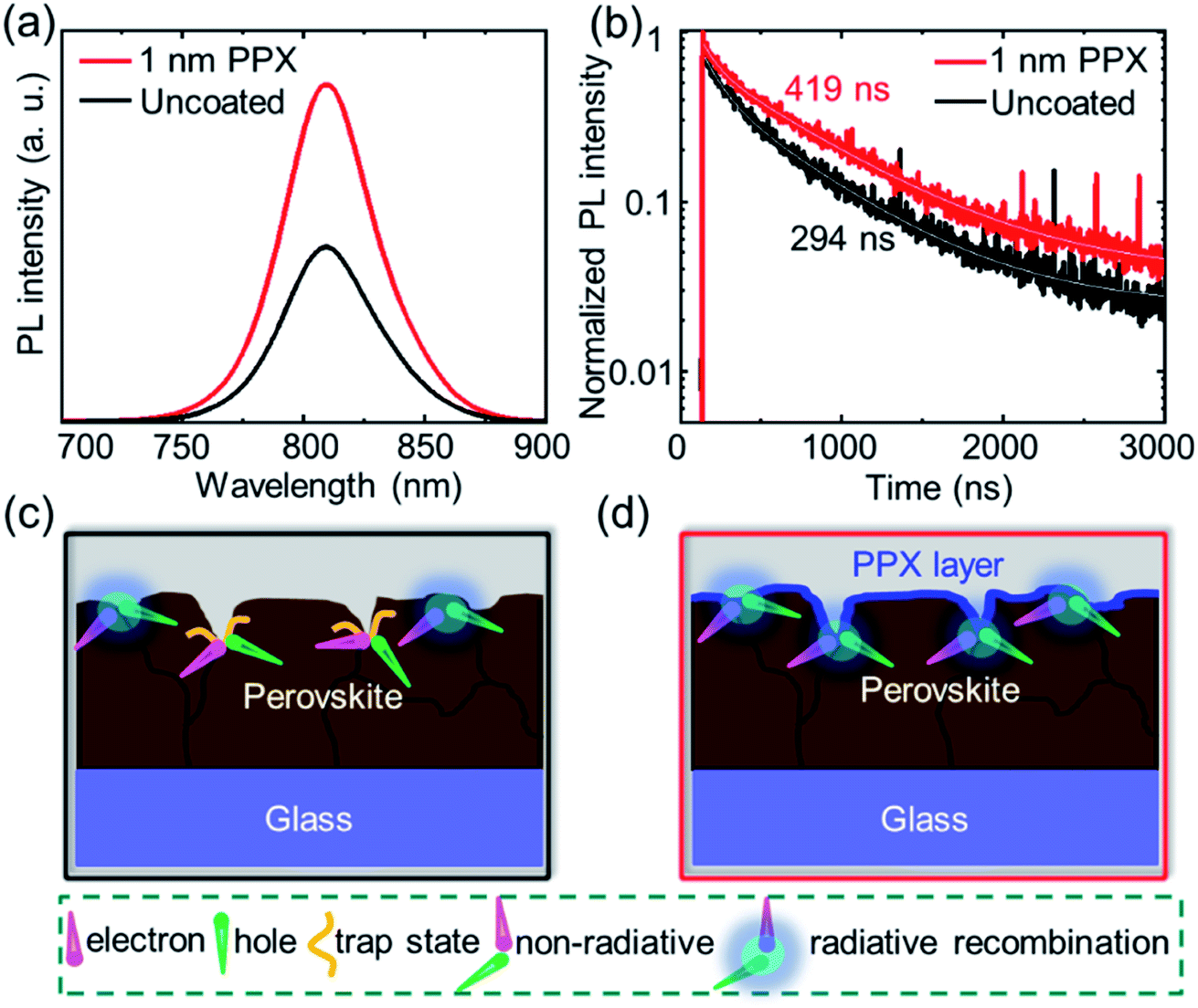 | ||
| Fig. 3 (a) Steady state photoluminescence (PL) and (b) time resolved PL (TRPL) of the uncoated and 1 nm PPX-coated perovskite films. Schematics of the charge carrier dynamics at the surface of the (c) uncoated and (d) PPX-coated perovskite thin film. | ||
Previous studies on solution-processed polymer passivation of perovskite thin films reported on the improved stability against moisture-induced degradation of the PSCs using passivation layers.17,37,38 Moreover, it has been demonstrated that CVD encapsulation of MAPbI3 solar cells by poly(p-chloro-xylylene) (parylene-C) can significantly slow down the perovskite decomposition reaction in high humidity atmosphere.50 Owing to the hydrophobic behavior of parylene polymers, the stability of CVD-coated PPX perovskite thin films and their incorporation in PSCs is investigated in this work, as well. To investigate the stability of the PSCs, uncoated, 1 nm PPX-coated (providing the optimal photovoltaic performance), and 5 nm PPX-coated (providing the thickest barrier layer) perovskite thin films are selected for further characterizations.
Measurements of the water contact angles (CA) confirm an increase in CA of perovskite thin films from 71 ± 4° for uncoated to 89 ± 4°, and 91 ± 5° for 1 nm and 5 nm PPX-coated respectively (Fig. S16†). The morphology of perovskite thin films (deposited on glass/ITO/SnO2 NPS) for 24 h in the ambient atmosphere (relative humidity ∼40–50%) under dark condition is investigated. For this purpose, atomic force microscopy (AFM) images of the exact same grains at the surface of uncoated, 1 nm and 5 nm PPX-coated perovskite thin films are measured at several time intervals (Fig. S17†). By comparing the morphology of the uncoated perovskite thin film at the beginning (0 h) to its morphology after 24 h, a very strong degradation is identified. Several small particles are formed on the surface of the perovskite grains (see marked areas in Fig. 4a), increasing their surface roughness (Fig. S18†). Several studies correlated the moisture-induced degradation starting at the surface of the grains and grain boundaries of perovskite thin film and identified the smaller particles appearing on the grains as PbI2.62–64 In stark contrast, not only 5 nm PPX-coated, but also 1 nm PPX-coated perovskite thin film exhibits no noticeable degradation in AFM images during the investigated 24 h (Fig. 4b and c) as well as almost the same surface roughness values (Fig. S18†) of the sample at 0 h and after 24 h. Notably, this is another evidence of the homogeneous PPX deposition by CVD polymerization because even the ultra-thin (1 nm) PPX layer protects conformably the rough surface of the perovskite thin film. Moreover, XRD analyses of the 1 nm and 5 nm PPX-coated perovskite films reveals no change in the PbI2 peak intensity (12.8°), while the uncoated perovskite thin film exhibits a strong increment in PbI2 after storage in ambient atmosphere for 24 h (Fig. 4d–f).
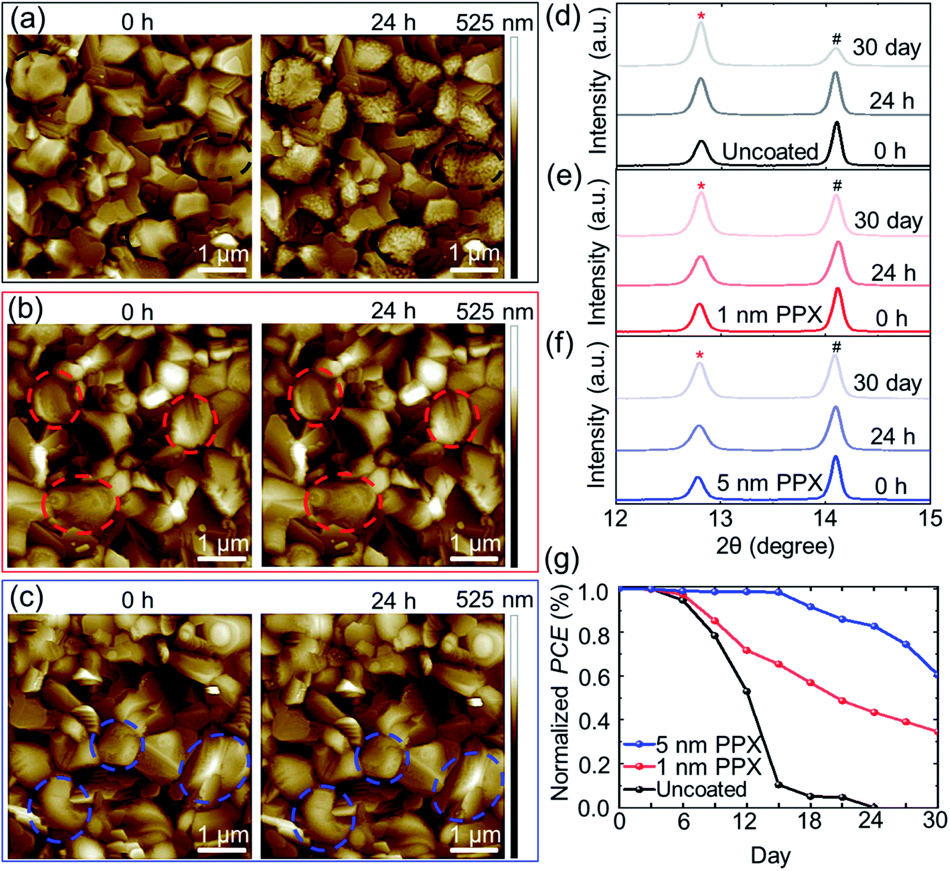 | ||
| Fig. 4 AFM height images of the (a) uncoated, (b) 1 nm PPX and (c) 5 nm PPX-coated perovskite thin films measured at 0 h and after 24 h exposure to ambient air conditions (relative humidity ∼40–50%). (d, e and f) XRD pattern of the uncoated perovskite thin film and the perovskite thin films coated with 1 nm and 5 nm PPX measured at 0 h, 24 h, and after 30 days exposure to ambient air conditions. (g) Stability tracking of PSCs without and with PPX passivation by exposing PSCs incorporated with the uncoated, 1 nm and 5 nm PPX-coated perovskite thin films to ambient atmosphere over 30 days. | ||
By increasing the storage time of the perovskite thin films up to 30 days, the PbI2 peak intensity in the XRD signal is increased further for the uncoated perovskite thin film and a slight increase for the 1 nm PPX-coated perovskite film is observed. Interestingly, for the 5 nm PPX-coated perovskite thin film, the change in the PbI2 peak is even less. This finding implies that an increase of the thickness of the polymer layer on top of perovskite thin film enhances the barrier properties against moisture, but sacrifices the PCE due to the poor conductivity of thicker PPX layers.
Having demonstrated that the PPX passivation films act as barriers47,65,66 for moisture ingress, the stability of unencapsulated PSCs with PPX passivation is examined by exposing PSCs incorporated with the uncoated, 1 nm and 5 nm PPX-coated perovskite thin films to ambient atmosphere (relative humidity ∼40–50%) and measuring repetitively the PCE over 30 days (Fig. 4g). It is observed that the uncoated PSC degrades completely after 24 days, while the PSCs with 1 nm and 5 nm PPX-coated, preserved 35% and 60% of their initial PCEs over 30 days. The photographs of PSCs with uncoated and the PPX-coated (1 nm and 5 nm) perovskite thin film at day 1 and at day 30 of the stability test are shown in Fig. S19.† The PSC with uncoated perovskite thin film is fully degraded and decomposed to PbI2 (yellow appearance given bandgap of ∼2.3 eV), but the PSCs with 1 nm and 5 nm PPX-coated still have the brown color of the perovskite thin film in the solar cell active area after 30 days. However, it is not possible to significantly increase the thickness of the PPX passivation layer on top of perovskite thin film to improve the stability of PSCs, given the insulating nature of the PPX layer can significantly decrease the PCE (see Fig. 2a–d).
In order to unambiguously prove that the PPX layer acts predominantly as a barrier against moisture, bare perovskite thin films with 1 nm and 5 nm thick PPX passivation layer, as well as reference perovskite thin films without PPX layers are exposed to severe humidity condition in a climate chamber (75% humidity, dark, 25 °C, 10 days). The XRD analyses after 10 days reveals that uncoated samples strongly degrade and produce the degradation product PbI2 (peak position 12.8°), while the degradation is strongly delayed for samples coated with PPX passivation layers (Fig. S20a–c†). Moreover, PSCs processed subsequent to this stress from perovskite thin films with PPX passivation layer demonstrate respectable PCE around 15% (Fig. S20d†). This analysis shows that PPX passivation layers predominantly act as barriers against moisture and, thereby, can enhance the stability of PSCs, which is in consistent with the long-term stability test of PSCs (Fig. 4g). Therefore, this work proposes the extension of the application of CVD-processed PPX layer to more intrinsically stable perovskites with a different composition such as triple cation mixed halides66 or two-dimensional Ruddlesden–Popper perovskites,66,67 which are more stable than the perovskite used in this work.
Conclusions
In this work, CVD polymerization is introduced as a novel technique to efficiently passivate the surface of polycrystalline perovskite thin films with ultra-thin PPX polymer layers. By means of photoluminescence spectroscopy, the improved surface passivation of perovskite thin films coated with PPX layers is demonstrated. The quality and thicknesses of PPX layers (<5 nm) are investigated by XPS, ToF-SIMS, and ellipsometry. Double-cation perovskite solar cells with PPX passivation layers of optimized thickness exhibit lower non-radiative surface recombination losses, resulting in an enhanced VOC (∼40 mV) and an improved FF. The champion solar cell using an optimal PPX passivation layer thickness of 1 nm shows a remarkable PCE of 20.4% and a stabilized power output PCE of around 19% for MPP tracking of 300 s. Furthermore, PSCs incorporating the PPX passivation layer show improved stability against moisture compared to uncoated perovskite thin films. In summary, this work reports on a novel, effective passivation strategy for perovskite photovoltaics using an innovative, scalable and precise deposition technique. However further work may result in more efficient and/or stable solar cells.Author contributions
M. M. B. and F. B. S. share equal contribution for conceiving the idea, developing the CVD PPX layer passivation and processing of the perovskite solar cells. A. A. E. was involved in the fabrication of the PSCs. V. T. conducted the XPS measurements and A. W. conducted the ToF-SIMS measurements. S. T., I. M. H., M. R. K. and J. A. S. conducted the optoelectronic and photovoltaics characterization. A. F. designed the stability test of PSCs. All co-authors discussed the paper and revised the manuscript. U. W. P., J. L. and F. B. S. were involved in designing the experiments and supervised the work.Conflicts of interest
The authors declare no conflict of interest.Acknowledgements
The authors gratefully acknowledge financial support of the German Federal Ministry of Education and Research (PRINTPERO, funding code: 03SF0557A), the German Federal Ministry for Economic Affairs and Energy (CAPITANO, funding code: 03EE1038B), and the Initiating and Networking funding of the Helmholtz Association (HYIG of U. W. P. (funding code: VH-NG1148); Recruitment Initiative of B. S. R.; the Helmholtz Energy Materials Foundry (HEMF); PEROSEED (funding code: ZT-0024); and the Science and Technology of Nanostructures Research Program), the Soft Matter Synthesis Lab, and the Karlsruhe School of Optics & Photonics (KSOP).Notes and references
- A. Kojima, K. Teshima, Y. Shirai and T. Miyasaka, J. Am. Chem. Soc., 2009, 131, 6050–6051 CrossRef CAS.
- H. Min, M. Kim, S.-U. Lee, H. Kim, G. Kim, K. Choi, J. H. Lee and S. Il Seok, Science, 2019, 366, 749–753 CrossRef CAS.
- E. H. Jung, N. J. Jeon, E. Y. Park, C. S. Moon, T. J. Shin, T. Y. Yang, J. H. Noh and J. Seo, Nature, 2019, 567, 511–515 CrossRef CAS.
- R. Schmager, J. Roger, J. A. Schwenzer, F. Schackmar, T. Abzieher, M. Malekshahi Byranvand, B. Abdollahi Nejand, M. Worgull, B. S. Richards and U. W. Paetzold, Adv. Funct. Mater., 2020, 30, 1907481 CrossRef CAS.
- M. Saliba, T. Matsui, J.-Y. Seo, K. Domanski, J.-P. Correa-Baena, M. K. Nazeeruddin, S. M. Zakeeruddin, W. Tress, A. Abate, A. Hagfeldt and M. Gratzel, Energy Environ. Sci., 2016, 9, 1989–1997 RSC.
- D. P. Mcmeekin, G. Sadoughi, W. Rehman, G. E. Eperon, M. Saliba, M. T. Hörantner, A. Haghighirad, N. Sakai, L. Korte, B. Rech, M. B. Johnston, L. M. Herz and H. J. Snaith, Science, 2016, 351, 151–155 CrossRef CAS.
- W. Nie, H. Tsai, R. Asadpour, J.-C. Blancon, A. J. Neukirch, G. Gupta, J. J. Crochet, M. Chhowalla, S. Tretiak, M. a. Alam, H.-L. Wang and A. D. Mohite, Science, 2015, 347, 522–525 CrossRef CAS.
- M. M. Byranvand, S. Song, L. Pyeon, G. Kang, G. Y. Lee and T. Park, Nano Energy, 2017, 34, 181–187 CrossRef CAS.
- S. Ternes, T. Börnhorst, J. A. Schwenzer, I. M. Hossain, T. Abzieher, W. Mehlmann, U. Lemmer, P. Scharfer, W. Schabel, B. S. Richards and U. W. Paetzold, Adv. Energy Mater., 2019, 9, 1901581 CrossRef CAS.
- J. Peng, Y. Wu, W. Ye, D. a. Jacobs, H. Shen, X. Fu, Y. Wan, T. Duong, N. Wu, C. Barugkin, H. T. Nguyen, D. Zhong, J. Li, T. Lu, Y. Liu, M. N. Lockrey, K. J. Weber, K. R. Catchpole and T. P. White, Energy Environ. Sci., 2017, 10, 1792–1800 RSC.
- H. Kim, S. U. Lee, D. Y. Lee, M. J. Paik, H. Na, J. Lee and S. Il Seok, Adv. Energy Mater., 2019, 9, 1902740 CrossRef CAS.
- J. J. Yoo, S. Wieghold, M. C. Sponseller, M. R. Chua, S. N. Bertram, N. T. P. Hartono, J. S. Tresback, E. C. Hansen, J. P. Correa-Baena, V. Bulović, T. Buonassisi, S. S. Shin and M. G. Bawendi, Energy Environ. Sci., 2019, 12, 2192–2199 RSC.
- H. Taherianfard, G.-W. Kim, F. Ebadi, T. Abzieher, K. Choi, U. W. Paetzold, B. S. Richards, A. Alrhman Eliwi, F. Tajabadi, N. Taghavinia and M. Malekshahi Byranvand, ACS Appl. Mater. Interfaces, 2019, 11, 44802–44810 CrossRef CAS.
- Best research-cell efficiencies, https://www.nrel.gov/pv/assets/pdfs/best-research-cell-efficiencies.20200218.pdf, accessed 2020-02-18 Search PubMed.
- Q. Jiang, Y. Zhao, X. Zhang, X. Yang, Y. Chen, Z. Chu, Q. Ye, X. Li, Z. Yin and J. You, Nat. Photonics, 2019, 13, 460–466 CrossRef CAS.
- X. Zheng, B. Chen, J. Dai, Y. Fang, Y. Bai, Y. Lin, H. Wei, X. C. Zeng and J. Huang, Nat. Energy, 2017, 2, 17102 CrossRef CAS.
- M. Kim, S. G. Motti, R. Sorrentino and A. Petrozza, Energy Environ. Sci., 2018, 11, 2609–2619 RSC.
- J. A. Christians, P. A. Miranda Herrera and P. V. Kamat, J. Am. Chem. Soc., 2015, 137, 1530–1538 CrossRef CAS.
- J. Lee, M. Malekshahi Byranvand, G. Kang, S. Y. Son, S. Song, G.-W. Kim and T. Park, J. Am. Chem. Soc., 2017, 139, 12175–12181 CrossRef CAS.
- W. Li, W. Zhang, S. Van Reenen, R. J. Sutton, J. Fan, A. A. Haghighirad, M. B. Johnston, L. Wang and H. J. Snaith, Energy Environ. Sci., 2016, 9, 490–498 RSC.
- S. S. Shin, E. J. Yeom, W. S. Yang, S. Hur, M. G. Kim, J. Im, J. Seo, J. H. Noh and S. Il Seok, Science, 2017, 356, 167–171 CrossRef CAS.
- T. Abzieher, S. Moghadamzadeh, F. Schackmar, H. Eggers, F. Sutterlüti, A. Farooq, D. Kojda, K. Habicht, R. Schmager, A. Mertens, R. Azmi, L. Klohr, J. A. Schwenzer, M. Hetterich, U. Lemmer, B. S. Richards, M. Powalla and U. W. Paetzold, Adv. Energy Mater., 2019, 9, 1802995 CrossRef.
- W. Zhang, J. Xiong, L. Jiang, J. Wang, T. Mei, X. Wang, H. Gu, W. A. Daoud and J. Li, ACS Appl. Mater. Interfaces, 2017, 9, 38467–38476 CrossRef CAS.
- T. Niu, J. Lu, R. Munir, J. Li, D. Barrit, X. Zhang, H. Hu, Z. Yang, A. Amassian, K. Zhao and S. Liu, Adv. Mater., 2018, 30, 1706576 CrossRef.
- F. Giordano, A. Abate, J. P. Correa Baena, M. Saliba, T. Matsui, S. H. Im, S. M. Zakeeruddin, M. K. Nazeeruddin, A. Hagfeldt and M. Graetzel, Nat. Commun., 2016, 7, 1–6 Search PubMed.
- M. M. Byranvand, T. Kim, S. Song, G. Kang, S. U. Ryu and T. Park, Adv. Energy Mater., 2018, 8, 1702235 CrossRef.
- H. Tan, A. Jain, O. Voznyy, X. Lan, F. P. G. de Arquer, J. Z. Fan, R. Quintero-Bermudez, M. Yuan, B. Zhang, Y. Zhao, F. Fan, P. Li, L. N. Quan, Y. Zhao, Z.-H. Lu, Z. Yang, S. Hoogland and E. H. Sargent, Science, 2017, 355, 722–726 CrossRef CAS.
- K. Choi, J. Lee, H. Il Kim, C. W. Park, G.-W. Kim, H. Choi, S. Park, S. A. Park and T. Park, Energy Environ. Sci., 2018, 11, 3238–3247 RSC.
- P. Schulz, D. Cahen and A. Kahn, Chem. Rev., 2019, 119, 3349–3417 CrossRef CAS.
- S. Akin, N. Arora, S. M. Zakeeruddin, M. Grätzel, R. H. Friend and M. I. Dar, Adv. Energy Mater., 2019, 2, 1–29 Search PubMed.
- D. Koushik, W. J. H. Verhees, Y. Kuang, S. Veenstra, D. Zhang, M. A. Verheijen, M. Creatore and R. E. I. Schropp, Energy Environ. Sci., 2017, 10, 91–100 RSC.
- J. Zhuang, P. Mao, Y. Luan, X. Yi, Z. Tu, Y. Zhang, Y. Yi, Y. Wei, N. Chen, T. Lin, F. Wang, C. Li and J. Wang, ACS Energy Lett., 2019, 2913–2921 CrossRef CAS.
- F. Tan, H. Tan, M. I. Saidaminov, M. Wei, M. Liu, A. Mei, P. Li, B. Zhang, C. S. Tan, X. Gong, Y. Zhao, A. R. Kirmani, Z. Huang, J. Z. Fan, R. Quintero-Bermudez, J. Kim, Y. Zhao, O. Voznyy, Y. Gao, F. Zhang, L. J. Richter, Z. H. Lu, W. Zhang and E. H. Sargent, Adv. Mater., 2019, 31, 1807435 CrossRef.
- F. Wang, A. Shimazaki, F. Yang, K. Kanahashi, K. Matsuki, Y. Miyauchi, T. Takenobu, A. Wakamiya, Y. Murata and K. Matsuda, J. Phys. Chem. C, 2017, 121, 1562–1568 CrossRef CAS.
- J. Peng, J. I. Khan, W. Liu, E. Ugur, T. Duong, Y. Wu, H. Shen, K. Wang, H. Dang, E. Aydin, X. Yang, Y. Wan, K. J. Weber, K. R. Catchpole, F. Laquai, S. De Wolf and T. P. White, Adv. Energy Mater., 2018, 8, 1801208 CrossRef.
- Q. Wang, Q. Dong, T. Li, A. Gruverman and J. Huang, Adv. Mater., 2016, 28, 6734–6739 CrossRef CAS.
- M. Li, X. Yan, Z. Kang, Y. Huan, Y. Li, R. Zhang and Y. Zhang, ACS Appl. Mater. Interfaces, 2018, 10, 18787–18795 CrossRef CAS.
- B. Chaudhary, A. Kulkarni, A. K. Jena, M. Ikegami, Y. Udagawa, H. Kunugita, K. Ema and T. Miyasaka, ChemSusChem, 2017, 10, 2473–2479 CrossRef CAS.
- F. Yang, H. E. Lim, F. Wang, M. Ozaki, A. Shimazaki, J. Liu, N. B. Mohamed, K. Shinokita, Y. Miyauchi, A. Wakamiya, Y. Murata and K. Matsuda, Adv. Mater. Interfaces, 2018, 5, 1701256 CrossRef.
- K. C. K. Cheng, M. A. Bedolla-Pantoja, Y.-K. Kim, J. V Gregory, F. Xie, A. De France, C. Hussal, K. Sun, N. L. Abbott and J. Lahann, Science, 2018, 362, 804–808 CrossRef CAS.
- H.-Y. Chen and J. Lahann, Langmuir, 2011, 27, 34–48 CrossRef CAS.
- M. E. Alf, A. Asatekin, M. C. Barr, S. H. Baxamusa, H. Chelawat, G. Ozaydin-lnce, C. D. Petruczok, R. Sreenivasan, W. E. Tenhaeff, N. J. Trujillo, S. Vaddiraju, J. Xu and K. K. Gleason, Adv. Mater., 2010, 22, 1993–2027 CrossRef CAS.
- J. Lahann, Polym. Int., 2006, 55, 1361–1370 CrossRef CAS.
- A. M. Ross, D. Zhang, X. Deng, S. L. Chang and J. Lahann, Anal. Chem., 2011, 83, 874–880 CrossRef CAS.
- J. A. Schwenzer, L. Rakocevic, R. Gehlhaar, T. Abzieher, S. Gharibzadeh, S. Moghadamzadeh, A. Quintilla, B. S. Richards, U. Lemmer and U. W. Paetzold, ACS Appl. Mater. Interfaces, 2018, 10, 16390–16399 CrossRef CAS.
- J. Lee, T. H. Lee, M. M. Byranvand, K. Choi, H. Il Kim, S. A. Park, J. Y. Kim and T. Park, J. Mater. Chem. A, 2018, 6, 5538–5543 RSC.
- W. F. Gorham, J. Polym. Sci., Part A-1: Polym. Chem., 1966, 4, 3027–3039 CrossRef CAS.
- X. Deng and J. Lahann, J. Appl. Polym. Sci., 2014, 131, 40315 CrossRef.
- H.-Y. Chen, J. H. Lai, X. Jiang and J. Lahann, Adv. Mater., 2008, 20, 3474–3480 CrossRef CAS.
- H. Kim, J. Lee, B. Kim, H. R. Byun, S. H. Kim, H. M. Oh, S. Baik and M. S. Jeong, Sci. Rep., 2019, 9, 15461 CrossRef.
- Q. Jiang, Z. Chu, P. Wang, X. Yang, H. Liu, Y. Wang, Z. Yin, J. Wu, X. Zhang and J. You, Adv. Mater., 2017, 29, 1703852 CrossRef.
- Q. Jiang, L. Zhang, H. Wang, X. Yang, J. Meng, H. Liu, Z. Yin, J. Wu, X. Zhang and J. You, Nat. Energy, 2016, 2, 16177 CrossRef.
- S. Gharibzadeh, B. Abdollahi Nejand, M. Jakoby, T. Abzieher, D. Hauschild, S. Moghadamzadeh, J. A. Schwenzer, P. Brenner, R. Schmager, A. A. Haghighirad, L. Weinhardt, U. Lemmer, B. S. Richards, I. A. Howard and U. W. Paetzold, Adv. Energy Mater., 2019, 9, 1803699 CrossRef.
- Y. S. Jeong, B. Ratier, A. Moliton and L. Guyard, Synth. Met., 2002, 127, 189–193 CrossRef CAS.
- E. L. Unger, E. T. Hoke, C. D. Bailie, W. H. Nguyen, A. R. Bowring, T. Heumüller, M. G. Christoforo and M. D. McGehee, Energy Environ. Sci., 2014, 7, 3690–3698 RSC.
- O. Hentz, P. Rekemeyer and S. Gradečak, Adv. Energy Mater., 2018, 8, 1701378 CrossRef.
- T.-H. Han, S. Tan, J. Xue, L. Meng, J.-W. Lee and Y. Yang, Adv. Mater., 2019, 31, 1803515 CrossRef CAS.
- K. Tvingstedt, L. Gil-Escrig, C. Momblona, P. Rieder, D. Kiermasch, M. Sessolo, A. Baumann, H. J. Bolink and V. Dyakonov, ACS Energy Lett., 2017, 2, 424–430 CrossRef CAS.
- C. M. Wolff, P. Caprioglio, M. Stolterfoht and D. Neher, Adv. Mater., 2019, 31, 1902762 CrossRef CAS.
- W. Tress, M. Yavari, K. Domanski, P. Yadav, B. Niesen, J. P. Correa Baena, A. Hagfeldt and M. Graetzel, Energy Environ. Sci., 2018, 11, 151–165 RSC.
- E. Aydin, M. De Bastiani and S. De Wolf, Adv. Mater., 2019, 31, 1900428 CrossRef.
- C. C. Boyd, R. Cheacharoen, T. Leijtens and M. D. McGehee, Chem. Rev., 2019, 119, 3418–3451 CrossRef CAS.
- J. S. Yun, J. Kim, T. Young, R. J. Patterson, D. Kim, J. Seidel, S. Lim, M. A. Green, S. Huang and A. Ho-Baillie, Adv. Funct. Mater., 2018, 28, 1705363 CrossRef.
- M. A. Spivack, Rev. Sci. Instrum., 1970, 41, 1614–1616 CrossRef CAS.
- T.-N. Chen, D.-S. Wuu, C.-C. Wu, C.-C. Chiang, Y.-P. Chen and R.-H. Horng, Plasma Processes Polym., 2007, 4, 180–185 CrossRef CAS.
- M. Saliba, T. Matsui, K. Domanski, J.-Y. Seo, A. Ummadisingu, S. M. Zakeeruddin, J.-P. Correa-Baena, W. R. Tress, A. Abate, A. Hagfeldt and M. Grätzel, Science, 2016, 354, 206–209 CrossRef CAS.
- H. Tsai, W. Nie, J. C. Blancon, C. C. Stoumpos, R. Asadpour, B. Harutyunyan, A. J. Neukirch, R. Verduzco, J. J. Crochet, S. Tretiak, L. Pedesseau, J. Even, M. A. Alam, G. Gupta, J. Lou, P. M. Ajayan, M. J. Bedzyk, M. G. Kanatzidis and A. D. Mohite, Nature, 2016, 536, 312–317 CrossRef CAS.
Footnotes |
| † Electronic supplementary information (ESI) available. See DOI: 10.1039/d0ta06646j |
| ‡ These authors contributed equally to this work. |
| This journal is © The Royal Society of Chemistry 2020 |