DOI:
10.1039/D0TA05859A
(Paper)
J. Mater. Chem. A, 2020,
8, 16366-16375
New frontier in printed thermoelectrics: formation of β-Ag2Se through thermally stimulated dissociative adsorption leads to high ZT†
Received
12th June 2020
, Accepted 17th July 2020
First published on 17th July 2020
Abstract
Printed thermoelectrics (TE) could significantly reduce the production cost of energy harvesting devices by large-scale manufacturing. However, developing a high performance printable TE material is a substantial challenge. In this work, a new one-pot synthesis and processing of high performance Ag2Se based n-type printed TE materials is reported. Structural analyses reveal that orthorhombic β-Ag2Se is the dominant phase in the n-type printed material compounds. For a printed material at room temperature, a breakthrough power-factor of ∼17 μW cm−1 K−2 with a record high figure-of-merit ZT ∼ 1.03 is achieved. A high average ZT, an important parameter for device applications, of ∼0.85–0.60 has been realized in the temperature range of 300 K to 400 K. Using this material for n-type legs in combination with commercially available PEDOT:PSS for p-type legs, a printed TE generator (print-TEG) of two thermocouples has been fabricated. An output voltage of 17.6 mV and a high maximum power output Pmax of 0.19 μW are achieved using the print-TEG at ΔT = 75 K.
1. Introduction
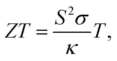
Thermoelectric (TE) generators are a promising technology for large-scale waste heat recovery and for harvesting energy from ambient heat sources to power small electronic devices. The maximum efficiency with which conversion from thermal to electrical energy takes place is largely dependent on the used materials' figure-of-merit ZT values, denoted by1
where S stands for the Seebeck coefficient, σ is the electrical conductivity, κ denotes the thermal conductivity, and T is the temperature of the material. While conventional TE materials prepared by solid-state techniques achieve on average higher ZT values, printable TE inks have their advantages in their superior processing and upscaling properties.2 This enables mass production of low-cost roll-to-roll printed flexible TE devices for a variety of applications ranging from wearable electronics3 to large area waste heat recovery. One way to develop TE inks is embedding the TE bulk material as a powder in a passive matrix of additives and solvents. The resulting printable composite can then be printed through various printing techniques, e.g., screen printing or ink-jet printing, onto mechanically flexible substrates and subsequently sintering them.4–6 However, development of printable thermoelectric inks resulting in high efficiencies is a key challenge in the field. The rheological adaptation of TE inks to the different printing techniques by introducing non-conductive additives and solvents oftentimes leads to an overall reduced ZT value compared with the base thermoelectric material.7 Chemical instability with respect to the additives, the solvents, and the ambient air can further deteriorate the electronic properties. Furthermore, many TE inks require a high sintering temperature which would destroy the underlying flexible polymer substrate. Hence, while the best conventional bulk TE materials are reported to have ZT values exceeding 2, it is very difficult to achieve even a ZT of 0.5 in a printed TE material through moderate temperature annealing processes.8–10 Bi2Te3 based n- and p-type bulk TE materials have been targeted extensively to make them printable while preserving their high performance at room temperature (RT).11–13 Unfortunately, the disruption of charge carrier transport at the interfaces of the particles in a printed film due to binders and additives diminishes the overall thermoelectric performance.14 Recently, an Sb2Te3 based flexible printed film with a ZT of 1 was reported to be achieved through connecting Bi0.4Sb1.6Te3 particles by melted Te particles.15 However, an intermediate post-printing high pressing process and high sintering temperature of 723 K make this approach infeasible for large-scale production.4 In an alternative approach, a power factor value of 3.63 μW cm−1 K−2 with ZT over 0.2 was attained in a screen-printed Bi2Te3 film through interface modification.6 Inkjet printed Bi2Te3 and Bi0.5Sb1.5Te3 flexible nanowires were reported to reach power factors of 1.80 μW cm−1 K−2 and 1.10 μW cm−1 K−2, respectively, through post-print thermal annealing.16 Organic materials on the other hand offer a much easier path towards printability. In particular, conductive polymers have attracted much attention recently because of their promising printability with high σ and low κ, but the low S values limit their thermoelectric performance. A p-type PEDOT:PSS [poly(3,4-ethylenedioxythiophene):polystyrene sulfonate] based conductive polymer was reported to exhibit good performance mainly due to low κ and high σ.17 However, despite being used worldwide,7 PEDOT:PSS based polymers with similar performances have not been reproduced or reported by any other researcher so far. Different approaches, hybridization and functionalization are being put forward to improve the TE performance of printable conductive polymers like n-type 1,1,2,2-ethenetetrathiolate (ett)–metal coordination polymers poly[Ax(M–ett)] (A = K, Na; M = Ni, Cu) and p-type PEDOT18–25 but the performance is still well below that of their inorganic counterparts.
In this work we overcome the significant reduction of electrical conductivity resulting in a low figure-of-merit caused by the separation of inorganic particles by binders and additives in a printed TE material. To this end, a new facile one-pot synthesis paradigm is introduced to prepare Ag2Se based printed materials without defined grain boundaries through a post-printing moderate temperature thermal annealing process. Bulk Ag2Se chalcogenides are known to exhibit high TE performance at RT.26 In addition, through dissociative adsorption of Se by Ag, the Ag2Se phase is formed at lower temperatures, beneficial for printing technology.27 Previously, various other intricate methods, for example magnetron sputtering28 and vacuum-assisted filtration,29–31 have been used to prepare high performance flexible Ag2Se TE films. We have recently reported an n-type Ag–Se based printed film with ZT ∼ 0.6 where the ink was made of silver paste and Se particles. However, the figure-of-merit was still not up to the mark and the use of commercial silver paste makes this process costly.32 Here, we present a high-performance n-type Ag2Se based printed material with ZT ∼ 1 at RT. This is to the best of our knowledge the highest reported ZT value for a printed TE material to date. The one-pot synthesis using raw Ag and Se powder is very simple, allowing easy upscaling to industrial batch sizes. Furthermore, the post-printing sintering temperature of 473 K is low enough that it does not destroy the flexible substrate foils made of commercial polymers such as polyethylene terephthalate (PET). We also demonstrate the operation of a printed TE generator (print-TEG) made of the Ag2Se based material for n-type legs in combination with commercial PEDOT:PSS as p-type legs.
2. Experimental methods
2.1. Materials
Se powder (100 mesh, ≥99.5% trace metal basis, Sigma Aldrich), Ag powder (2–3.5 μm, ≥99.9% trace metal basis, Sigma Aldrich), polystyrene (average Mw ∼ 192![[thin space (1/6-em)]](https://www.rsc.org/images/entities/char_2009.gif) 000, Sigma Aldrich) as a binder, toluene (anhydrous, 99.8%, Sigma Aldrich) as a solvent, and BYK additive were used.
000, Sigma Aldrich) as a binder, toluene (anhydrous, 99.8%, Sigma Aldrich) as a solvent, and BYK additive were used.
2.2. One-pot synthesis of TE inks
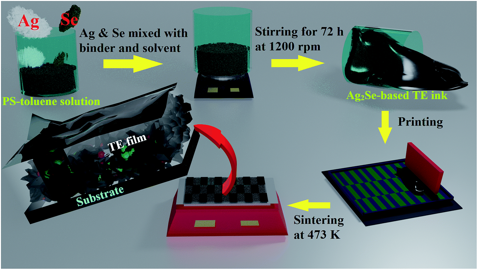
Multiple printable inks were prepared by mixing Ag and Se powders in different weight ratios together with ∼2 wt% BYK additive in a polystyrene–toluene solution (6:94 in wt ratio) followed by stirring the mixture for 72 h at 1200 rpm. The wt% of Se in the material (1 − x)Ag–xSe was varied from 10 to 60% (0.1 ≤ x ≤ 0.6) in order to optimize their TE performance. We kept the weight ratio of (1 − x)Ag–xSe to the solvent in the inks constantly at 1:1. The films were prepared on glass substrates/measurement chips using manual doctor blading or screen printing followed by sintering at 473 K, a temperature near the melting point of Se, for a duration of 5–10 min in ambient air. In order to modify the rheology of the film for different printing techniques, extra additives were added with the inks without affecting the charge transport. The screen printability of the TE ink on a flexible PEN substrate has been checked using a semi-automatic ROKUPRINT machine. A routine of the preparation of Ag2Se based printable TE inks and films is demonstrated in Fig. 1.
 |
| | Fig. 1 The different steps to the synthesis of printable TE ink and to prepare printed TE films. | |
2.3. Analysis of materials and TE parameters
The Seebeck coefficient (S) and electrical conductivity (σ) of the printed films on glass substrates at RT were determined using a custom-built set-up. In addition, temperature dependent thermoelectric parameters S, σ and the in-plane thermal conductivity (κ) of the printed films of thicknesses 25–40 μm in the temperature range of RT to 450 K were measured using a Linseis thin film analyzer (TFA) system. The measurement setup was developed by V. Linseis et al. based on the method presented by Völklein et al.33–35 The experimental errors related to the TE parameters, S, σ and κ measured using the TFA system are ∼7%, 6%, and 10%, respectively. The Hall carrier concentration (nH) was calculated from the Hall coefficient (RH) measured using the Linseis Hall measurement setup. Phase and crystallographic structures of the printed films at different temperatures were analysed by the X-ray diffraction (XRD) technique in Bragg–Brentano geometry using Ni filtered Cu-Kα1,2 lines on a Bruker D8 diffractometer with a Lynxeye XE detector and an Anton Paar HTK1200 heating chamber. Morphological and microstructural analyses were done using a focused ion beam scanning electron microscope (FIB-SEM) (ZEISS Auriga 60). Elemental distribution and composition were analysed by energy dispersive X-ray spectroscopy (EDS) (EDAX). Thicknesses of the printed films were determined using BRUKER 3D microscopes based on a white light interferometer (WLI). The screen-printability of the optimized ink was checked using a semi-automatic flat-screen ROKUPRINT printing machine. A printed TE generator (print-TEG) of two thermocouples was fabricated using the printed material as n-type legs in combination with commercially available PEDOT:PSS PH1000 for printing the p-type legs. The performance of the print-TEG was characterised using a custom-built set-up.
3. Results and discussion
3.1. Crystallographic and microstructure analysis
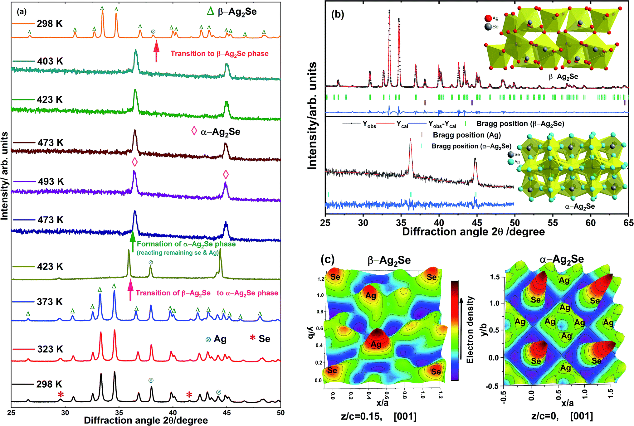
Phase and crystallographic structures of the printed films (1 − x)Ag–xSe for x = 0.20, 0.27 and 0.40 were determined by XRD analysis. The RT XRD patterns of the printed films sintered at 473 K indicate the formation of the orthorhombic β-Ag2Se phase along with a small fraction of excess Ag or Se (Fig. S1, ESI†). Excess Ag and Se are found to be significant together with the orthorhombic β-Ag2Se phase in the printed films for x = 0.20 and 0.40 respectively. For the stoichiometric film with x = 0.27 we found predominantly the orthorhombic β-Ag2Se phase along with a small amount of unreacted Ag. In order to track the formation and the crystallographic transitions of the Ag2Se phase with changing temperature, XRD analysis of an as-prepared stoichiometric printed film was performed during heating and cooling in the temperature range of 298 to 493 K (cf.Fig. 2(a)). Initially, the non-sintered printed film is found to be a mixed phase comprising the orthorhombic β-Ag2Se phase with unreacted Se and Ag at 298 K. This indicates that Se and Ag have reacted partially to form the β-Ag2Se phase during the long stirring process through dissociative adsorption of Se by Ag. This is in agreement with a previous report.27 The existing orthorhombic β-Ag2Se phase is transformed into the high temperature cubic α-Ag2Se phase at 423 K, which is in agreement with the temperature dependent heat capacity (CP) results (Fig. S3, ESI†). The remaining unreacted Se is found to be adsorbed by Ag forming the single cubic α-Ag2Se phase at 473 K and it remains in the same phase up to 493 K. During cooling, the cubic α-Ag2Se phase remains unchanged down to 403 K and is transformed to the orthorhombic β-Ag2Se phase at RT. In order to get more insights into the crystallographic structure of the RT orthorhombic β-Ag2Se phase and high-temperature cubic α-Ag2Se phase, Rietveld refinement of the XRD patterns of the printed films was done using the FULLPROF program. The refinement results with diffraction patterns and refinement parameters are shown in Fig. 2(b) and Table 1 respectively. The structural analysis of the RT XRD pattern using Rietveld refinement reveals that the printed film corresponds to the main phase, β-Ag2Se, which belongs to the space group P212121 along with 2.32 vol% of excess Ag (cf.Fig. 2(b)). The lattice constants of the β-Ag2Se phase are calculated to be a = 0.433(1) nm, b = 0.706(3) and c = 0.777(0) nm. Both Ag and Se atoms in the β-Ag2Se crystal lattice are found to occupy Wyckoff position 4a (x, y, z). The crystal structure of the printed film at 473 K is found to be the cubic α-Ag2Se phase belonging to the space group Im![[3 with combining macron]](https://www.rsc.org/images/entities/char_0033_0304.gif) m. The Ag and Se atoms of the cubic α-Ag2Se phase are located in the two inequivalent positions 12d (1/4, 1/2, 0) and 2a (0, 0, 0), respectively, with the lattice parameter a = 0.496(2) nm.
m. The Ag and Se atoms of the cubic α-Ag2Se phase are located in the two inequivalent positions 12d (1/4, 1/2, 0) and 2a (0, 0, 0), respectively, with the lattice parameter a = 0.496(2) nm.
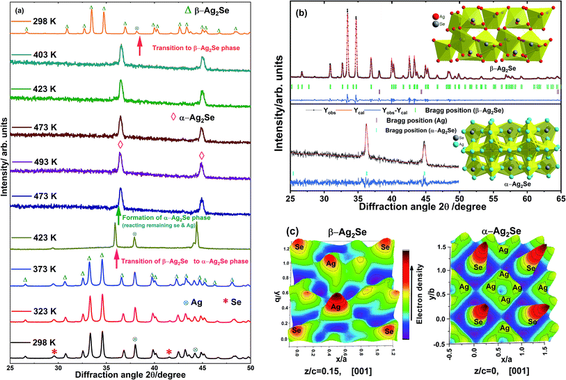 |
| | Fig. 2 Temperature dependent XRD patterns of the printed film for x = 0.27 during heating and cooling (a). β-Ag2Se is found to be the primary phase at room temperature and it transforms to the α-Ag2Se phase at T > 423 K. Rietveld refinement results and XRD patterns for the room temperature orthorhombic β-Ag2Se and high temperature cubic α-Ag2Se phase together with their crystal structures (b). The Fourier maps for electron density distributions of the atoms, Ag and Se, for β-Ag2Se and α-Ag2Se phases (c). | |
Table 1 The crystal structure parameters of β-Ag2Se and α-Ag2Se phases determined by Rietveld refinement of the XRD patterns
| Crystallographic phases |
Lattice parameters, nm |
Wyckoff positions |
Space groups |
|
a
|
b
|
c
|
4a |
12d |
2a |
| β-Ag2Se. |
0.433(1) |
0.706(3) |
0.777(0) |
Ag, Se |
— |
— |
P212121 |
| α-Ag2Se |
0.496(2) |
0.496(2) |
0.496(2) |
— |
Ag |
Se |
Imm |
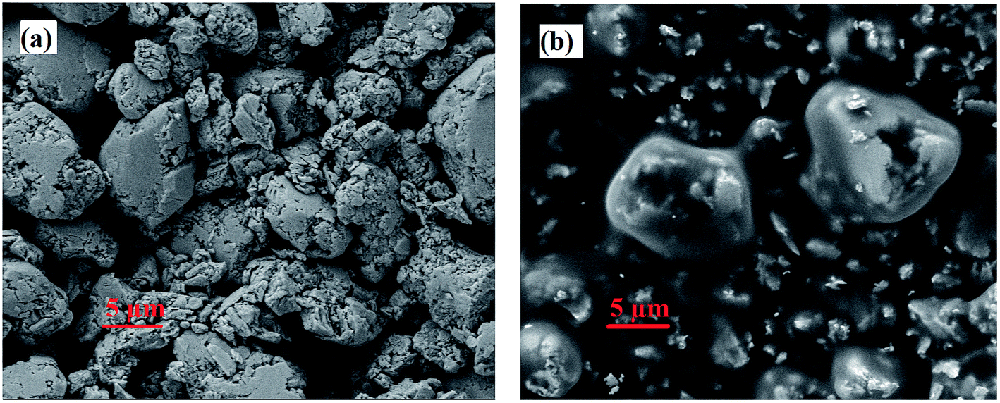
Three-dimensional Fourier maps along the [001] direction of the planes z/c = 0.15 and z/c = 0 for the orthorhombic β-Ag2Se phase and cubic α-Ag2Se phase, respectively, are shown in Fig. 2(c). Electron density distributions of the atoms, Ag and Se, can be visualised from the Fourier maps which indicate that the position of the Se atom for the β-Ag2Se phase on the z/c = 0.15 plane is x/a = 0.112, y/b = 0.998, and that for α-Ag2Se on the z/c = 0 plane is x/a = 0, y/b = 0. Microstructural images of the stoichiometric (x = 0.27) drop-cast films using FIB-SEM before and after sintering at 473 K for a few minutes are shown in Fig. 3(a) and (b) respectively. It is found that particles with dimensional size <10 μm are present in the film before sintering whereas the particles lose their definite shapes and appear agglomerated after sintering forming the Ag2Se phase through dissociative adsorption of Se by Ag (blackish region). The small fraction of greyish particles corresponds to Ag present in the sintered film due to insufficient sintering time for the elements to react fully. The particles look blurry due to the surrounding transparent polystyrene resin. When the printed films are sintered at 473 K, the polystyrene present in the film flows around the Ag and Se particles, and the Se becomes highly volatile and starts to be adsorbed by Ag to form the Ag2Se phase. As a result, dense films are formed. Using EDS analysis, elements present in the films and the atomic percentage of the elements were estimated. EDS analysis for both non-sintered and sintered films is given in Fig. S2 & Table S1, ESI.† EDS results indicate that both the films are stoichiometric with a slight deviation from the designed composition.
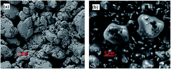 |
| | Fig. 3 The SEM microstructures of non-sintered (a) and sintered (b) film at 473 K for x = 0.27. Particles of dimension <10 μm are present in the non-sintered film which are found to react while sintering at 473 K. | |
3.2. Thermoelectric performance of the printed films
The TE performances of the printed films, (1 − x)Ag–xSe for 0.5 ≤ x ≤ 0.90 on glass substrates have been studied extensively in order to identify the optimum composition. TE transport parameters S and σ of the printed films have been measured at room temperature after sintering at 473 K in ambient air for 5 min and 10 min, cf.Fig. 4(a) and (b). The electrical conductivity σ is found to decrease whereas the magnitude of S increases with increasing wt% of Se in the composition. This is due to a decrease in the volume fraction of excess Ag and Ag2Se phase which leads to a decrease in carrier concentration in the films, cf.Fig. 4(c). nH is found to increase with increasing temperature in the complete temperature range for all compositions indicating the semiconducting nature of the material. However, the carrier concentration drops by 10 times when x changes from 0.20 to 0.27 and continues to decrease with increasing x due to nearly complete adsorption of Ag by Se. Considering that the single phase printed film with x = 0.27 follows the single parabolic band (SPB) model, the effective mass m* of the charge carrier is estimated using the following equation:36| | 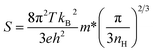 | (1) |
where h is Planck's constant and kB is the Boltzmann constant. RT m* is found to be 0.19me which is in agreement with the theoretically and experimentally calculated effective mass of β-Ag2Se in previous reports.37–39 The Hall carrier mobility (μH) is found to be ∼1100 cm2 V−1 s−1 at RT and both μH and m* decrease with increasing temperature as shown in Fig. 4(e). σ varies from 500 S cm−1 to 100 S cm−1 and the magnitude of S increases from 100 μV K−1 to 220 μV K−1, respectively for different compositions. Consequently, the power factor (S2σ) initially increases with increasing Se content and starts decreasing after reaching a maximum at a nearly stoichiometric composition. We observed that the films with compositions between x = 0.20 and 0.40 exhibit a high power factor value of ≥10 μW cm−1 K−2. Hence, temperature dependent thermoelectric properties of the printed films with x = 0.20, 0.27 and 0.40 have been studied in the range of 300 K to 450 K (cf.Fig. 5). Details of the measurement procedure and setup are described in ESI Fig. S4.† The electrical conductivities for all compositions increase with increasing temperature, showing a semiconducting behaviour. However, for the film with x = 0.40, σ decreases with increasing temperature at T > 400 K due to the interruption of carrier transport by the highly resistive volatilized excess Se. The films with x = 0.20 and 0.27 exhibit high absolute electrical conductivity for printed n-type materials whereas the film with x = 0.40 shows significantly lower electrical conductivity compared to the other two films in the complete temperature range. We attribute this to a decrease in carrier concentration due to an increase in Se wt%. Negative Seebeck coefficient values are found for all compositions indicating that majority charge carriers are n-type (cf.Fig. 5(b)). The magnitude of S is found to be high at room temperature and decreases at higher temperatures for all films, which is consistent with the variation of electrical conductivity with temperature. The film with x = 0.40 exhibits the highest S value of −210 μV K−1 which decreases with decreasing ‘x’ at RT. The temperature dependent power factor, S2σ, of all compositions calculated from S and σ, is shown in Fig. 5(d). The power factor for the stoichiometric film (x = 0.27) is found to be highest in the complete temperature range exhibiting a maximum value of ∼17 μW cm−1 K−2 at RT. The absolute value of the in-plane thermal conductivity, κ, of all the films is found to be low compared to bulk Ag2Se based materials and a weak temperature dependency is observed in the complete temperature range, as shown in Fig. 5(c). However, the thermal conductivity decreases with increasing Se wt% in the printed films because of the decrease in charge carrier concentration. In addition, upon Se doping, thermal conductivity is suppressed further due to point defect phonon scattering by the cluster of volatized Se. It is found that κ varies from 0.50 W m−1 K−1 to 0.31 W m−1 K−1 at 300 K for all compositions with x = 0.40 leading to the lowest value at all temperatures. The thermal conductivity of stoichiometric Ag2Se film (x = 0.27) is found to be 0.496 W m−1 K−1, which is lower compared to the κ values, ∼1 W m−1 K−1 for bulk Ag2Se.27,40,41 However, low thermal conductivity values of 0.64 and 0.449 W m−1 K−1 for flexible Ag2Se film not containing insulating resin have been reported in ref. 28 and 29. In our work, the low thermal conductivity value is due to reduced heat transfer in the presence of insulating polystyrene resin. Our data can be compared with published data on composite materials. It has been reported that the high thermal conductivity value (>200 W m−1 K−1) of aluminium nitride (AlN) can be reduced by more than 10 times by compositing with >40 vol% of polystyrene or other polymers.42–45 Assuming that the spherical Ag2Se particles are embedded in polystyrene resin, the low thermal conductivity of the films can be explained using the Bruggeman model. The thermal conductivity κ of a film comprising the Ag2Se phase and polystyrene can be expressed as46| | 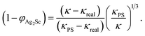 | (2) |
Here κ and κreal are the thermal conductivities of the printed film and the pure Ag2Se phase respectively, φAg2Se is the volume fraction of the Ag2Se phase and κPS is the thermal conductivity of polystyrene. κ is calculated using the estimated value of φAg2Se ∼ 0.65 in the printed film and the reported thermal conductivity of polystyrene κPS ∼ 0.15 W m−1 K−1.43 The resulting κ of the printed material is found to be 0.543 W m−1 K−1, which is in good agreement with the experimentally found value of 0.496 W m−1 K−1. In order to evaluate the lattice and electronic contribution κe to κ, we estimate the electronic contribution as follows: the Lorenz number L at RT is estimated using the equation47| | | L = 1.5 + exp[−|S|/116] | (3) |
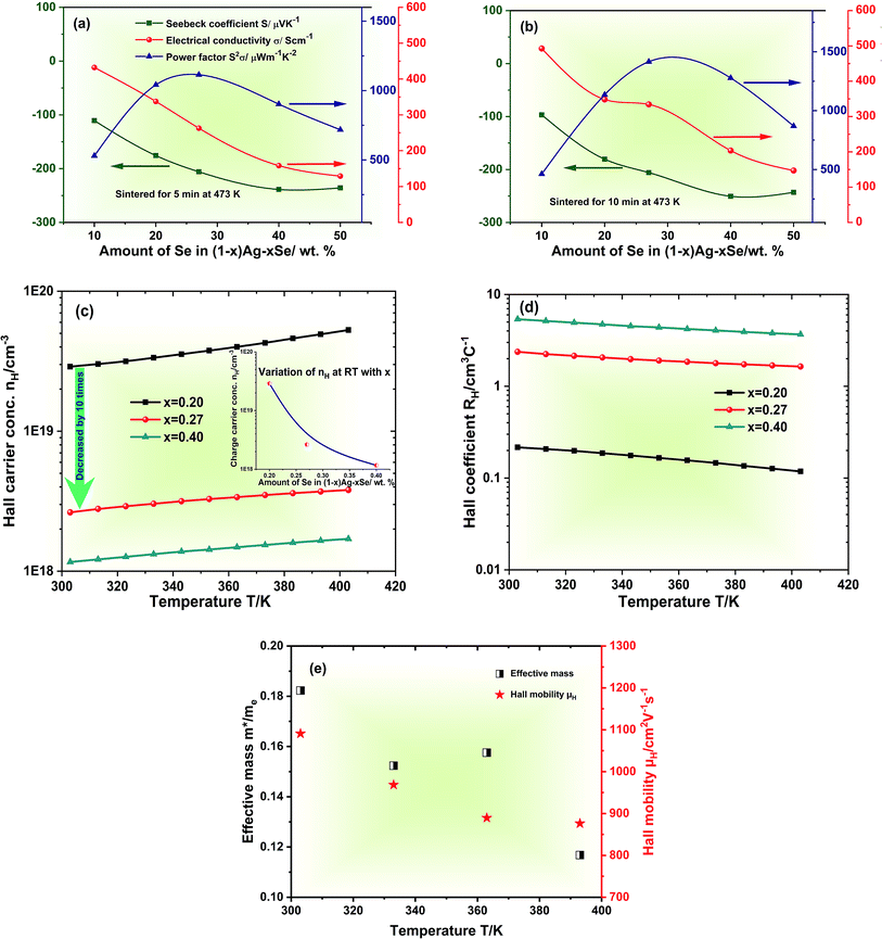 |
| | Fig. 4 Composition-dependent thermoelectric properties of the printed films sintered at 473 K for 5 min (a) and 10 min (b). The nearly stoichiometric compositions show higher power factors. The temperature-dependent Hall carrier concentration (nH) (c) and Hall coefficient (RH) (d) for the films with x = 0.2, 0.27, and 0.4. Variation of the effective mass (m*) and Hall mobility (μH) with temperatures of the film for x = 0.27 (e). | |
 |
| | Fig. 5 Variation of thermoelectric parameters σ (a), S (b) and κ (c) of the printed films for x = 0.20, 0.27 and 0.40 with temperatures from 300 to 450 K. The calculated power factor S2σ (d) and figure-of-merit ZT (e) for all the printed films. It is observed that the film with x = 0.27 shows the highest S2σ and ZT for all the temperatures. A comparison of room temperature ZT for different pressure treatment-free printed TE films is shown (f). To the best of our knowledge, the highest ZT ∼ 1 is achieved for a printed material at RT in this work. | |
For the three films the values of L are found to be between 1.65 × 10⁻⁸ W Ω K−2 and 1.75 × 10⁻⁸ W Ω K−2. The electronic and lattice thermal conductivity κe and κl at RT are calculated via the Wiedemann–Franz law, κe = σLT, see Fig. S5, ESI.†κe is found to contribute ∼50% to the total κ for x = 0.20 and 0.27 due to the higher electrical conductivity whereas it is significantly lower than κl for 0.40 contributing only ∼23%. The temperature dependent figures-of-merit ZT for all printed films are shown in Fig. 5(e). The stoichiometric film with x = 0.27 shows the highest ZT for all temperatures achieving an impressively high value of 1.03 at 300 K. A comparison of TE performances for different pressure treatment-free printed TE films is shown Fig. 5(f). TE performances of recently reported Ag2Se based films are also given in Table 2. A high average ZT, which is an important parameter for device applications, of ∼0.85–0.60 has also been estimated in the temperature range from 300 K to 400 K. The ink was found to be long-term stable leading to reproducible results (cf. Fig. S6, ESI†).
Table 2 Thermoelectric performances of different recently reported Ag2Se based films
| Ag2Se based films |
Preparation methods |
Power factor/μW cm−1 K−2 |
ZT
|
Reference |
| Ag2Se film on a nylon membrane |
Vacuum assisted filtration |
9.87 |
0.6 |
29
|
| Ag2Se/Ag/CuAgSe composite on a nylon membrane |
Vacuum assisted filtration |
22.3 |
∼0.5 |
30
|
| Ag–Se printed film |
Doctor blading |
5 |
0.6 |
32
|
| Ag2Se film on a nylon membrane |
Vacuum assisted filtration |
18.8 |
0.8 |
31
|
| Ag2Se thin film |
Magnetron sputtering |
24.4 |
1.2 |
28
|
3.3. Performance of a printed TEG
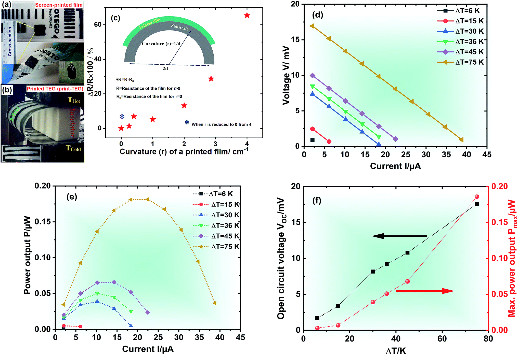
To demonstrate the printability and flexibility of the materials we first fabricate strips of our material on PEN-foil by doctor blading. The behaviour under bending conditions has been studied by measuring the change in the resistance of the film with increasing curvature (r) from 0 to 4 cm−1, as shown in Fig. 6(c). It is observed that up to 2 cm−1, the change in resistance is <20% and reaches ∼70% for r = 4 cm−1. However, the change in resistance is reversible to <10% again when the bending is relaxed (blue asterisks in Fig. 6(c)). Using the Ag2Se ink with x = 0.27 as n-type legs and commercially available PEDOT:PSS (PH1000) (S, σ and κ at RT are measured to be 25.4 μV K−1, 368 S cm−1 and 1.56 W m−1 K−1, respectively) as p-type legs, a printed TE generator (print-TEG) with dimensions ∼8.5 cm × 3.6 cm × 0.015 cm was fabricated. The print-TEG is made of two thermocouples and has been fabricated manually by doctor blading the two materials on a 75 μm PEN substrate (cf.Fig. 6(b)) followed by sintering at 473 K for 10 min. For measuring the device performance, the print-TEG has been characterized by varying the device current from 0 to 45 μA and the temperature difference ΔT from 6 to 75 K, while measuring the output voltage with a KEITHLEY Source Measuring Unit 2601B. Hereby the two ends of the device were thermally coupled to the hot and cold side of a measuring setup using thermal conductive paste and separated by an insulating block (cf.Fig. 6(b)). The device performance is shown in Fig. 6(d). The open circuit voltage VOC and the maximum power output Pmax are found to be 17.6 mV and 0.19 μW for ΔT = 75 K. The Seebeck coefficient per thermocouple estimated from the VOC value is found to be significantly low as compared to the material Seebeck coefficient while the TEG is operated. The most likely reason is that the thermal contact resistance when tracking the maximum power point of the TEG plays a role and leads to a reduced thermovoltage. To check the screen printability of the TE ink, it was printed on a flexible PEN substrate using a semi-automatic ROKUPRINT machine, shown in Fig. 6(a).
 |
| | Fig. 6 Screen printed Ag2Se film with cross-section image taken using an optical microscope in the inset (a). The print-TEG of two thermocouples during operation (b). Study of the flexibility of the printed film: change in the resistance of the film with increasing curvature (c). Performance of the print-TEG operating at different temperatures (d–f). The print-TEG exhibits an output voltage of 17.6 mV and a high maximum power output Pmax of 0.19 μW for ΔT = 75 K. | |
4. Conclusion
In this work, high performance n-type Ag2Se based printed TE materials have been developed through a scalable one-pot synthesis process. Unlike the conventional approach, the orthorhombic β-Ag2Se TE phase revealed by structural analyses is formed after printing by thermal annealing at moderate temperature due to the dissociative adsorption of volatilized Se by Ag particles. Hence, a high conductivity transport path of Ag2Se without defined grain boundaries is created. As a result, a record high figure-of-merit ZT > 1 with a high average ZT of ∼0.94 is attained at room temperature in the printed material. A printed TE generator of two thermocouples yields an output voltage of 17.6 mV with a high maximum power output Pmax of 0.19 μW for ΔT = 60 K. The results are found to be reproducible and repeatable and the TE generator is stable in air for a month demonstrating its potential for industrial applications.
Conflicts of interest
There are no conflicts to declare.
Acknowledgements
The authors wish to acknowledge the Deutsche Forschungsgemeinschaft (DFG, German Research Foundation) under Germany's Excellence Strategy via the Excellence Cluster 3D Matter Made to Order (EXC-2082/1 – 390761711) for financial support. The authors wish to acknowledge funding by the Ministry of Science, Research and Arts of the state of Baden Württemberg through the MERAGEM graduate school. This work was also supported by the German Federal Environmental Foundation (Deutsche Bundesstiftung Umwelt – DBU) through the DBU PhD scholarship program.
References
- H. S. Kim, W. Liu, G. Chen, C.-W. Chu and Z. Ren, Proc. Natl. Acad. Sci. U. S. A., 2015, 112, 8205–8210 CrossRef CAS PubMed.
- J. Kim, R. Kumar, A. J. Bandodkar and J. Wang, Adv. Electron. Mater., 2017, 3, 1600260 CrossRef.
- A. Nozariasbmarz, H. Collins, K. Dsouza, M. H. Polash, M. Hosseini, M. Hyland, J. Liu, A. Malhotra, F. M. Ortiz, F. Mohaddes, V. P. Ramesh, Y. Sargolzaeiaval, N. Snouwaert, M. C. Özturk and D. Vashaee, Appl. Energy, 2020, 258, 114069, DOI:10.1016/J.apenergy.2019.114069.
- S. Shin, R. Kumar, J. W. Roh, D. S. Ko, H. S. Kim, S. Il Kim, L. Yin, S. M. Schlossberg, S. Cui, J. M. You, S. Kwon, J. Zheng, J. Wang and R. Chen, Sci. Rep., 2017, 7, 7317, DOI:10.1038/s41598-017-07654-2.
- K. Wu, Y. Yan, J. Zhang, Y. Mao, H. Xie, J. Yang, Q. Zhang, C. Uher and X. Tang, Phys. Status Solidi RRL, 2017, 11, 1700067, DOI:10.1002/pssr.201700067.
- J. Feng, W. Zhu, Y. Deng, Q. Song and Q. Zhang, ACS Appl. Energy Mater., 2019, 2, 2828, DOI:10.1021/acsaem.9b00178.
- M. Orrill and S. LeBlanc, J. Appl. Polym. Sci., 2017, 134, 44256 CrossRef.
- L. D. Zhao, C. Chang, G. Tan and M. G. Kanatzidis, Energy Environ. Sci., 2016, 9, 3044–3060 RSC.
- H. J. Wu, L. D. Zhao, F. S. Zheng, D. Wu, Y. L. Pei, X. Tong, M. G. Kanatzidis and J. Q. He, Nat. Commun., 2014, 5, 4515, DOI:10.1038/ncomms5515.
- B. Srinivasan, A. Gellé, F. Gucci, C. Boussard-Pledel, B. Fontaine, R. Gautier, J. F. Halet, M. J. Reece and B. Bureau, Inorg. Chem. Front., 2019, 6, 63–73, 10.1039/c8qi00703a.
- S. J. Kim, J. H. We, J. S. Kim, G. S. Kim and B. J. Cho, J. Alloys Compd., 2014, 582, 177–180, DOI:10.1016/j.jallcom.2013.07.195.
- J. H. We, S. J. Kim, G. S. Kim and B. J. Cho, J. Alloys Compd., 2013, 552, 107–110, DOI:10.1016/j.jallcom.2012.10.085.
- J. H. We, S. J. Kim and B. J. Cho, Energy, 2014, 73, 506–512, DOI:10.1016/j.energy.2014.06.047.
- Z. Cao, E. Koukharenko, M. J. Tudor, R. N. Torah and S. P. Beeby, J. Phys.: Conf. Ser., 2013, 476, 012031, DOI:10.1088/1742-6596/476/1/012031.
- T. Varghese, C. Dun, N. Kempf, M. Saeidi-Javash, C. Karthik, J. Richardson, C. Hollar, D. Estrada and Y. Zhang, Adv. Funct. Mater., 2020, 30, 1905796, DOI:10.1002/adfm.201905796.
- B. Chen, M. Kruse, B. Xu, R. Tutika, W. Zheng, M. D. Bartlett, Y. Wu and J. C. Claussen, Nanoscale, 2019, 11, 5222–5230, 10.1039/c8nr09101c.
- G. H. Kim, L. Shao, K. Zhang and K. P. Pipe, Nat. Mater., 2013, 12, 719–723, DOI:10.1038/nmat3635.
- B. T. McGrail, A. Sehirlioglu and E. Pentzer, Angew. Chem., Int. Ed., 2015, 54, 1710–1723, DOI:10.1002/anie.201408431.
- M. He, F. Qiu and Z. Lin, Energy Environ. Sci., 2013, 6, 1352–1361 RSC.
- Q. Wei, M. Mukaida, K. Kirihara, Y. Naitoh and T. Ishida, Materials, 2015, 8, 732–750 CrossRef CAS PubMed.
- D. Kim, Y. Kim, K. Choi, J. C. Grunlan and C. Yu, ACS Nano, 2010, 4, 513–523, DOI:10.1021/nn9013577.
- O. Bubnova, Z. U. Khan, A. Malti, S. Braun, M. Fahlman, M. Berggren and X. Crispin, Nat. Mater., 2011, 10, 429–433, DOI:10.1038/nmat3012.
- Y. Sun, L. Qiu, L. Tang, H. Geng, H. Wang, F. Zhang, D. Huang, W. Xu, P. Yue, Y. S. Guan, F. Jiao, Y. Sun, D. Tang, C. A. Di, Y. Yi and D. Zhu, Adv. Mater., 2016, 28, 3351–3358, DOI:10.1002/adma.201505922.
- L. Liu, Y. Sun, W. Li, J. Zhang, X. Huang, Z. Chen, Y. Sun, C. Di, W. Xu and D. Zhu, Mater. Chem. Front., 2017, 1, 2111–2116, 10.1039/c7qm00223h.
- Y. Sun, P. Sheng, C. Di, F. Jiao, W. Xu, D. Qiu and D. Zhu, Adv. Mater., 2012, 24, 932–937, DOI:10.1002/adma.201104305.
- H. Z. Duan, Y. L. Li, K. P. Zhao, P. F. Qiu, X. Shi and L. D. Chen, JOM, 2016, 68, 2659–2665, DOI:10.1007/s11837-016-1980-4.
- D. Yang, X. Su, F. Meng, S. Wang, Y. Yan, J. Yang, J. He, Q. Zhang, C. Uher, M. G. Kanatzidis and X. Tang, J. Mater. Chem. A, 2017, 5, 23243–23251, 10.1039/c7ta08726h.
- J. A. Perez-Taborda, O. Caballero-Calero, L. Vera-Londono, F. Briones and M. Martin-Gonzalez, Adv. Energy Mater., 2018, 8, 1702024, DOI:10.1002/aenm.201702024.
- Y. Ding, Y. Qiu, K. Cai, Q. Yao, S. Chen, L. Chen and J. He, Nat. Commun., 2019, 10, 841, DOI:10.1038/s41467-019-08835-5.
- Y. Lu, Y. Qiu, K. Cai, Y. Ding, M. Wang, C. Jiang, Q. Yao, C. Huang, L. Chen and J. He, Energy Environ. Sci., 2020, 13, 1240–1249, 10.1039/c9ee01609k.
- C. Jiang, Y. Ding, K. Cai, L. Tong, Y. Lu, W. Zhao and P. Wei, ACS Appl. Mater. Interfaces, 2020, 12, 9646–9655, DOI:10.1021/acsami.9b21069.
- M. M. Mallick, A. Roesch, L. Franke, S. Ahmad, A. Gall, H. Geßwein, J. Aghassi-Hagmann and U. Lemmer, ACS Appl. Mater. Interfaces, 2020, 12, 19655–19663, DOI:10.1021/acsami.0c01676.
- V. Linseis, F. Völklein, H. Reith, R. Hühne, L. Schnatmann, K. Nielsch and P. Woias, Semicond. Sci. Technol., 2018, 33, 085014, DOI:10.1088/1361-6641/aacf39.
- F. Völklein, H. Reith and A. Meier, Phys. Status Solidi A, 2013, 210, 106–118, DOI:10.1002/pssa.201228478.
- V. Linseis, F. Völklein, H. Reith, P. Woias and K. Nielsch, J. Mater. Res., 2016, 31, 20, DOI:10.1557/jmr.2016.353.
- J. P. Heremans, V. Jovovic, E. S. Toberer, A. Saramat, K. Kurosaki, A. Charoenphakdee, S. Yamanaka and G. J. Snyder, Science, 2008, 321, 554–557 CrossRef CAS PubMed.
- C. M. Fang, R. A. De Groot and G. A. Wiegers, J. Phys. Chem. Solids, 2002, 63, 457–464, DOI:10.1016/S0022-3697(01)00160-3.
- T. Day, F. Drymiotis, T. Zhang, D. Rhodes, X. Shi, L. Chen and G. Jeffrey Snyder, J. Mater. Chem. C, 2013, 1, 7568–7573, 10.1039/c3tc31810a.
- V. V. Gorbachev and I. M. Putilin, Phys. Status Solidi B, 1975, 69, K153–K156, DOI:10.1002/pssb.2220690266.
- M. Ferhat and J. Nagao, J. Appl. Phys., 2000, 88, 813, DOI:10.1063/1.373741.
- W. Mi, P. Qiu, T. Zhang, Y. Lv, X. Shi and L. Chen, Appl. Phys. Lett., 2014, 104, 133903, DOI:10.1063/1.4870509.
- G. Pezzotti, I. Kamada and S. Miki, J. Eur. Ceram. Soc., 2000, 20, 1197–1203, DOI:10.1016/S0955-2219(99)00282-4.
- S. Yu, P. Hing and X. Hu, Composites, Part A, 2002, 33, 289–292, DOI:10.1016/S1359-835X(01)00107-5.
- A. Agrawal and A. Satapathy, Composites, Part A, 2014, 63, 51–58, DOI:10.1016/j.compositesa.2014.04.001.
- G. Wu, Y. Wang, K. Wang and A. Feng, RSC Adv., 2016, 6, 102542–102548, 10.1039/c6ra22794e.
- R. C. Progelhof, J. L. Throne and R. R. Ruetsch, Polym. Eng. Sci., 1976, 16, 615–625 CrossRef CAS.
- H. S. Kim, Z. M. Gibbs, Y. Tang, H. Wang and G. J. Snyder, APL Mater., 2015, 3, 041506, DOI:10.1063/1.4908244.
Footnote |
| † Electronic supplementary information (ESI) available. CCDC 2017753 (β-Ag2Se) and 2017754 (α-Ag2Se). For ESI and crystallographic data in CIF or other electronic format see DOI: 10.1039/d0ta05859a |
|
| This journal is © The Royal Society of Chemistry 2020 |
Click here to see how this site uses Cookies. View our privacy policy here. 
 Open Access Article
 This Open Access Article is licensed under a Creative Commons Attribution-Non Commercial 3.0 Unported Licence
 *a,
Andres Georg
Rösch
a,
Leonard
Franke
a,
Andre
Gall
a,
Sarfraz
Ahmad
b,
Holger
Geßwein
b,
Andrey
Mazilkin
*a,
Andres Georg
Rösch
a,
Leonard
Franke
a,
Andre
Gall
a,
Sarfraz
Ahmad
b,
Holger
Geßwein
b,
Andrey
Mazilkin