
 Open Access Article
 This Open Access Article is licensed under a Creative Commons Attribution-Non Commercial 3.0 Unported Licence
Electro-chemo-mechanical effect in Gd-doped ceria thin films with a controlled orientation†
Simone
Santucci
 *a,
Haiwu
Zhang
a,
Simone
Sanna
b,
Nini
Pryds
a and
Vincenzo
Esposito
*a
*a,
Haiwu
Zhang
a,
Simone
Sanna
b,
Nini
Pryds
a and
Vincenzo
Esposito
*a
aDepartment of Energy Conversion and Storage, Technical University of Denmark, Fysikvej, Building 310, 2800 Kgs. Lyngby, Denmark. E-mail: sisan@dtu.dk; vies@dtu.dk
bDipartimento di Ingegneria Civile e Ingegneria Informatica and CNR-SPIN, Università di Roma Tor Vergata, Via del Politecnico 1, I-00133 Roma, Italy
First published on 30th June 2020
Abstract
Gd-doped ceria (CGO) fluorite exhibits prominent electro-chemo-mechanical properties and giant-electrostriction at room temperature and has been recently disclosed in both CGO polycrystalline films and bulk. The electromechanical properties of CGO depend on the oxygen vacancy defects of the fluorite lattice. Early experiments suggest that defects along the [111] crystallographic direction promote high atomic distortion. These factors result in the largest electrostriction response ever measured. However, only out-of-plane electrostriction (i.e. M13) in (111) CGO oriented thin films has been reported so far, and several questions remain open about the electrostriction mechanism in the oxygen-defective fluorite. Here, we present electromechanical performances along different crystallographic directions. We grow thin films by pulsed laser deposition on single crystal substrates to obtain longitudinal and shear deformations (i.e. M11 and M12) of highly coherent (100), (110) and (111) oriented CGO thin films. As a result, we find an order of magnitude higher electrostriction coefficient along [100]. Such an analysis gives a new insight into the mechanism of CGO electrostriction.
Introduction
Ceria-based materials are applied in a wide range of applications such as solid oxide fuel cells (SOFCs),1–3 oxygen sensors3,4 and storage,5 catalysts5–7 and memristors.8–10 Ceria oxide, i.e. CeO2−δ, is capable of accommodating a high amount of oxygen vacancies into the lattice, which results in its remarkable versatility as an ionic conductor and catalyst.11–13 At temperatures superior to 1200 °C (ref. 14) and low oxygen partial pressure (pO2 ≈ 2.5 × 10⁻³ atm),15 ceria undergoes a chemical reduction of Ce4+ to Ce3+ releasing oxygen gas and consequently increasing the defect concentration,
  .5,16 Acceptor doping, e.g. using substitutional rare-earth cations with a 3+ valence state (i.e. Gd, Nd, Sm, and La), stabilizes the structure and leads to high ionic mobility.2,7,17–21 At room temperature, doped ceria showed outstanding electromechanical properties due to local distortion in the vicinity of oxygen vacancies.22 Studies carried out on Gd-doped ceria (CGO) thin films,22–26 bulk27,28 and membranes,29–31 show an average electrostriction coefficient of Me ≈ 6 × 10⁻¹⁸ (m2 V−2),22 which is comparable to that of state-of-the-art materials such as Pb(Mn1/3Nb2/3)O3 (Me = 2 × 10⁻¹⁸ m2 V−2).32 For classical electrostrictors, Newnham et al. provided a relationship in which the logarithm of performances depends on (S/ε), where S is the elastic compliance and ε is the dielectric constant.33 However, Yavo et al.34 showed that the electromechanical properties of CGO are conflicting with the Newnham law. The electrostriction coefficient is two-three orders of magnitude higher than that of similar materials,35 meaning that a different mechanism is in play. In the same study, they also showed high electrostriction in (Y, Nb)-stabilized Bi2O3 bulk. These findings suggest that such features are common to some defective fluorite structures, representing a new family of electromechanical functional materials.
X-ray absorption spectroscopy (XAS) measurements on CGO attribute the electromechanical activity to the lattice distortion in the presence of oxygen vacancies.22,36,37 Although the dopant does not have an active role in the single lattice model,22,36 doping and vacancy association are able to influence the electrostriction in cerium oxide. In polycrystalline CGO, vacancies are mainly controlled by associations at the grain boundaries,38–40 which also act as ionic blocking barriers controlled by the dopant.17,38,41,42 Under an electric field, if the grain boundaries of a material have high resistivity, the voltage drops correspondingly. As a consequence, the overall electromechanical response drops.30 However, grain size is not directly related to electrostriction performances as reported in our recent work.27 We show that the electrostrictive behavior of polycrystalline CGO ceramics depends on the vacancy configurations within the grain boundaries. For these reasons, a grain boundary-free material is needed to obtain a clear insight into the sole lattice distortion effect.
To date, only the out-of-plane component of electrostriction i.e. M13 has been measured in thin films.23,43 Here, we apply a top planar electrode configuration which allows investigation of the other electrostriction directions of the matrix i.e. M11 and M12. By varying the crystal orientation of the film, we are able to study the crystal distortion in different crystallographic directions.
Fig. 1a shows the structural model proposed in previous studies to explain the macroscopic distortion of CGO thin films.22 Using the Kröger–Vink notation, we consider a 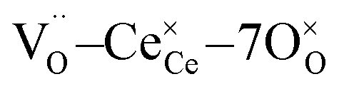 cell, where CeCe is the Ce4+ cation,
  is a vacancy located at an oxygen site, and 7OO denotes seven oxygen atoms. When the oxygen vacancy
 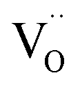 is included in a CGO cell
  , it causes the distortion of the unit, with a consequent rearrangement of the local elastic field and charge distribution. In particular, a distortion takes place by the elongation of the diagonal
 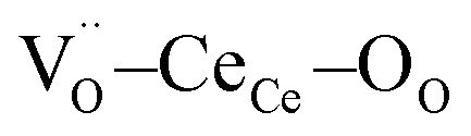 triplet (black vector), along the [111] direction. As a counter effect, the other six oxygen atoms collapse toward the center of the cell (blue vectors). As a consequence, the bonds of
  and CeCe–OO pairs along the diagonal are longer, while the remaining CeCe–6OO pairs are shorter. When an electric field is applied, the electroactive
  diagonal shrinks, and consequently it “squeezes out” the remaining six oxygen atoms in the perpendicular direction, yielding electrostriction. The model is confirmed by XAS experiments on thin films.36,37,44 Gd doping is needed to introduce a significant concentration of vacancies in the lattice, but it does not have an active role in the electrostrictive effect.22,36 Therefore, Gd was not considered in previous and current models.
 | ||
Fig. 1 CeO2 crystal structure with an oxygen vacancy inclusion. (a)  unit, structure of the current model for electrostriction in CGO. Black vector: unit, structure of the current model for electrostriction in CGO. Black vector:  electroactive triplet and distortion direction. Blue vectors: consequent 6O displacement. (b) 4-unit complex composed of four electroactive triplet and distortion direction. Blue vectors: consequent 6O displacement. (b) 4-unit complex composed of four  distorted units with a central vacancy. Near-empty site oxygen atoms, i.e. 6O, are numbered. Red lines highlight the bond direction of Ce atoms with oxygen 1 and 2. (c) 6O octahedral structure composed of six near-empty site oxygen atoms, base structure for our new model. distorted units with a central vacancy. Near-empty site oxygen atoms, i.e. 6O, are numbered. Red lines highlight the bond direction of Ce atoms with oxygen 1 and 2. (c) 6O octahedral structure composed of six near-empty site oxygen atoms, base structure for our new model. | ||
According to this interpretation, a field parallel to the [111] direction maximizes the electrostriction effect, as the most efficient way to induce strain of the  triplets.22,26 It is worth emphasizing that the model is based on thin film experiments, and it considers only a single cell, neglecting the surrounding structure.
In terms of the crystallographic arrangement, a larger surrounding region can be considered in the analysis. The oxygen atoms in the CGO lattice have a coordination number of 4, meaning that a single vacancy produces four  units. Fig. 1b shows a schematic illustration of the resulting complex. Under an electric field, all four
 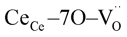 units rearrange simultaneously. In particular, six oxygen atoms (i.e. 6O, numbered in Fig. 1b) are bonded to two cations each, as illustrated for atom 1 and 2 (red lines). With an applied field, the 6O are expected to actively contribute to the lattice distortion as they withstand the force of two
  triplets at once. Moreover, they are the closest oxygen atoms to the
  site, which is the centre of the local elastic field and charge distortion. The 6O are arranged as an octahedron with the
 site placed in the centre, as illustrated in Fig. 1c.
A similar octahedron structural representation is used to describe the effect of local distortion in piezoelectric ABO3 perovskites. In such a structure, the oxygen atoms arrange as an octahedron with a central B-ion that induces stress.45–47 For piezoelectric perovskites, Li et al.46,47 also showed a trend of the distortion magnitude as a function of the electric field in the crystallographic directions. Such an analysis shows that an electric field parallel to 〈100〉 allows oxygen to release the stress imposed by the cation easily along the octahedron axis, favouring atomic distortion. Upon comparison, it can be seen that the displacement along the 〈110〉 directions results in an overall counteracting of the surrounding region, leading to a decreased electromechanical response. In the same manner, 〈111〉 directions show an even weaker distortion effect.46,47 On the other hand, the trend is opposite in fluorite structures such as CaF2.46
In this work, we use the pulsed laser deposition (PLD) technique to grow (100)-, (110)-, and (111)-oriented CGO grain boundary free thin films on (100)-oriented SrTiO3 (STO),2,48, (110) YSZ48,49 and (100) NdGaO3 (NGO)48,50,51 respectively. To study the electrostriction effect, we analyze both the longitudinal (M11) and the shear (M12) responses of the films as a function of the crystallographic orientation and the direction of the electric field. Then, we compare the experimental results with the microscopic model based on the ABO3 octahedron applied to CGO. As a result, we are able to provide new insight into the electrostrictive mechanics in the defective fluorite structure.
Experimental
Film and electrode deposition
We fabricated the Ce0.8Gd0.2O1.9 target from powder pressed at 140 MPa and then sintered at 1723 K for 10 h. XRD investigation indicated a pure fluorite phase of the target. One micron thick films of Ce0.8Gd0.2O1.9 were grown on STO(100), NGO(100) and YSZ(110) substrates by PLD using a KrF excimer laser (λ = 248 nm), at a 20 Hz repetition rate, 120 mJ energy and fluence of about 1.8 J cm−2 (deposition rate was ∼0.07 Å per pulse). During the deposition, we fixed the background oxygen pressure at 10−3 mbar, with a temperature of 600 °C. Such conditions were optimal for growing high-quality fluorite structured CGO with a single orientation.2,48 After deposition, the samples were kept in a chamber with the temperature slowly decreasing (−3 °C min−1) for reoxidation and releasing the stress. We sputtered Au top electrodes with a Bal-tec SCD 005 Sputter Coater at room temperature. The size of the substrates was 5 × 2.5 mm and the thickness was 0.1 mm.Sample characterization
We analysed the crystallographic properties of the grown samples using X-ray diffraction with a Rigaku Smartlab diffractometer. We carried out θ–2θ and rocking curve scans, and the crystalline quality of the film was established by evaluating the full-width-half-maximum (FWHM). Grazing incidence angle scans with α = 1° were performed on CGO/NGO to exclude the reflection of the substrate, as (100) NGO and (200) CGO reflection overlapped at ≈33° and confirmed the correct (111) orientation of the film. We analyzed the cross-section of the samples with a Zeiss Gemini-Merlin FE-SEM for microstructure and thickness measurements.Electrostriction setup
The electromechanical characterization was carried out on a cantilever with planar top electrodes. The samples had one side glued to a base, and the other one free to move. The experiment was performed at room temperature. The method used to calculate the electrostriction coefficient is reported in detail in the ESI.† We performed the measurements with a single-beam laser interferometer SIOS NA analyzer. The experimental setup and instruments are described elsewhere.23 However, we added some new features described here. The interferometer resolution was 5 pm, but the background noise is usually higher, and it was not possible to observe displacements smaller than 3–4 nm. We coupled an Ametek 7230 DSP Lock-in Amplifier to the interferometer. This instrument allowed us to extract an oscillating signal from the raw measurement of the SIOS NA analyzer. Since lock-in detection spots only periodically signal with a specific set frequency, the measured response is not affected by mechanical drift or external noise. As a consequence, when an oscillating field was applied, the resolution increased to values around 0.1–0.2 nm. These values were used as error bars in our measurements. The ESI† reports further details of the instrument and measurement data as an example (Fig. S2†). An AIM-TTI TGP 3100 function generator connected with a Trek 2220 amplifier, was used to apply a sinusoidal electric field to the samples. The voltage amplifier has been added to increase the electric field needed to trigger electrostriction on the samples with planar electrodes. The contacts were made with tungsten tips. Oscillation in electrostrictive materials always takes place with double the frequency of the applied field. For this reason, the source generator and the lock-in amplifier were set at 0.5 Hz and 1 Hz respectively. The displacement measured in this work was always related to the II harmonic contribution to the oscillation amplitude. A schematic of the updated experimental setup is reported in the ESI (Fig. S3†).Results and discussion
Structural characterization
We deposited highly coherent CGO thin films on several single-crystal substrates. Fig. 2 shows the results of the structural characterization, i.e. XRD pattern in θ–2θ scan mode, rocking curve and the microstructure of the thin films samples from scanning electron microscope (SEM) images. Depending on the orientation of the substrates, the films are grown in a single orientation, i.e. CGO(110)/YSZ(110), CGO(100)/STO(100) and CGO(111)/NGO(100) (Fig. 2a). The inset of the CGO(111)/NGO(100) plot shows a grazing angle scan to exclude the presence of CGO (200). For CGO(200)/STO(100), the cubic cell aligns along the [110] direction of the STO substrate and grows 45° in-plane tilted (Fig. S5†),2 resulting in an epitaxial relationship 〈110〉CGO//〈100〉STO in both in- and out-of-plane directions. | ||
| Fig. 2 Structural characterization of CGO(111)/NGO(100), CGO(100)/STO(100) and CGO(110)/YSZ(110) thin films. (a) θ–2θ scans of CGO(110)/YSZ(110) at the top, CGO(100)/STO(100) and CGO(111)/NGO(100) at the bottom. Inset: θ–2θ scan in grazing angle mode. (b) Rocking curve at the (220) peak of CGO on YSZ, (200) peak of CGO on STO and (111) peak of CGO on NGO. (c) Cross sectional images by SEM: from the top CGO(110)/YSZ(110), CGO(100)/STO(100) and CGO(111)/NGO(100). | ||
NGO is a perovskite with an orthorhombic cell. A pseudocubic structure with lattice parameter a ≈ 3.86 Å can be extracted.52 Considering an NGO substrate with the (200)orthorhombic orientation, a good crystallographic match is the (111) face of CGO50 with in-plane relationship [001]NGO//[0−11]CGO and [010]NGO//[−211]CGO. Finally, YSZ and CGO have similar cell parameters, and CGO grows on (110) YSZ with the in- and out-of-plane relationship 〈100〉CGO//〈100〉YSZ and 〈110〉CGO//〈110〉YSZ.48,49 More details of the film/substrate geometry can be found in the ESI.†Fig. 2b shows the rocking curve scans of CGO(111)/NGO(100), CGO(100)/STO(100) and CGO(110)/YSZ(110) with FWHM values of 0.42°, 0.32°, and 0.33° respectively. Such low values indicate a high order of crystallinity. The cross-section of the films (Fig. 2c) also shows a homogeneous and continuous microstructure without the signature of vertical grain boundaries, i.e. columnar grains. The samples are grown with a thickness of tf = 1 μm, ruling out the contribution from substrate-induced strain, which is relieved after a few nanometers.53 The lattice parameter of CGO, as determined from the XRD, indicates that the structures are fully relaxed pure fluorite.
Electrostriction effect and discussion
We evaluated the electromechanical performances by measuring the longitudinal M11 and the transverse M12 electrostriction coefficients. We used the cantilever vibration method23 on the samples with in-plane top electrodes (Fig. S1†). In CGO(111)/NGO(100), we used two different electrode configurations, as described in the ESI (Fig. S4†). By doing this, we can apply electric field along [−211] and [0−11] directions. In the same way, we apply voltage on CGO(110)/YSZ(110) along [001] and [−223] in-plane directions, as depicted in Fig. S6.† Fig. S1b† shows a typical map of the 2nd harmonic component of vertical displacement d in different positions on the sample. The X-scans and Y-scans indicate a distortion both parallel and perpendicular to the electric field, respectively.To measure the longitudinal electrostriction coefficient M11, we measure the displacement d in a fixed position for different electric fields. The scans along the width of the sample (Y-scans) allow evaluation of the shear component M12 (see the Experimental section for details).
Fig. 3 shows the electromechanical response of CGO thin films for both longitudinal and shear directions. Indications of the electric field direction are also reported. Fig. 3a shows the performances of CGO(110)/YSZ(110) in response to the electric field along the [001] direction. The longitudinal electrostriction coefficient is found to be M11 = 4.93 × 10⁻¹⁷ m2 V−2. Fig. 3c and e show the response of CGO(100)/STO(100) and CGO(111)/NGO(100) to the electric field along the [110] direction with a longitudinal electrostriction coefficient of 2.22 × 10⁻¹⁷ m2 V−2 and 3.50 × 10⁻¹⁸ m2 V−2, respectively. Fig. 3g shows the electric field in the CGO(111)/NGO(100) sample with in-plane electrodes is along the [−211] direction with an M11 = 2.03 × 10⁻¹⁸ m2 V−2. In CGO(110)/YSZ(110) with electrodes along the [−223] direction, the electrostriction is annihilated, and the oscillations are so weak to be comparable with the background noise. Therefore, we cannot calculate the electrostriction coefficient, and we report it as a minimal noise value M11 = <6.72 × 10⁻¹⁹ m2 V−2. Each measurement lasted between 5 and 10 minutes. We did not find evidence of degeneration of performances with time, evidencing the sound mechanical integrity of the device.23
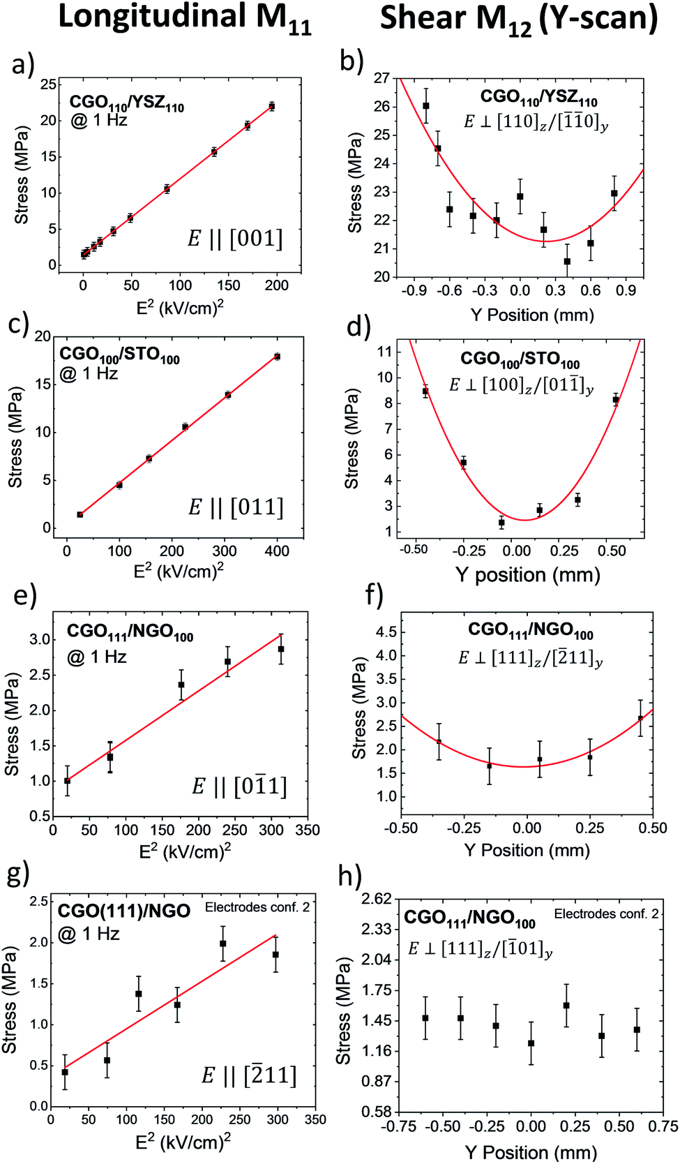 | ||
| Fig. 3 Electromechanical response of CGO thin films for different orientations and electric field direction at 1 Hz. The stress measured is the contribution to II harmonic of oscillation. First row: CGO (110) oriented on YSZ with electric field along [001] axis. (a) Longitudinal stress vs. electric field, used to calculate M11, (b) stress Y-scan, used to calculate M12. Second row: CGO (100) on STO with E∥[011]. (c) Longitudinal stress, (d) shear stress. Third row: CGO (111) on NGO with E∥[0−11]. (e) Longitudinal stress, (f) shear stress. Fourth row: CGO (111) on NGO with E∥[-211]. (g) Longitudinal stress, (h) shear displacement. | ||
According to eqn (S4),† the electrostriction coefficient is dependent on Young's modulus (Y) of CGO which was assumed to be 200 GPa.22,23,53–55 The Y values can change depending on the hkl texture, but such measurements are still not available in the literature. However, Goldsby et al. reported the elastic compliances of CeO2 by the first-principles simulation for different hkl,56 showing a maximum difference of 30% from the average value. Moreover, Young's modulus was obtained for fluorite structure YSZ,57,58 showing similar values along all the crystallographic directions. Kurpaska et al. in particular, reported Y ranging from 235 GPa along 〈110〉 to 216 GPa along with 〈111〉.58 Fujikane et al., on the other hand, showed variable Y depending on the experimental technique. They considered the nanoindentation method most trustable as they obtained Y with a maximum difference of 21% and 9% for elastic and elastoplastic deformation, respectively. Taking into account these results, we decided to use the approximated Y presented in the literature for a thin-film configuration.
Fig. 3b, d, f and h show the full Y-scans for M12 analysis as a result of laser profilometry measurements. We applied 13 kV cm−1 at a 1 Hz frequency. The transverse electrostriction coefficient represents the component of stress that is perpendicular to the electric field. As the electrostriction effect takes place in both in- and out-of plane directions, we describe the crystal distortion in terms of vertical and lateral directions. Fig. 3b shows the transverse electrostrictive response of CGO(110)/YSZ(110) with a measured value of M12 = 0.26 × 10⁻¹⁷ m2 V−2 considering the vertical (z) and in-plane (y) directions [110]z/[−1−10]y. On other hand, for the CGO(100)/STO(100) sample, the electrostriction coefficient is M12 = 0.79 × 10⁻¹⁷ m2 V−2 along [100]z/[0–11]y as depicted in Fig. 3d. CGO(111)/NGO(100) shows an electrostriction coefficient of M12 = 1.9 × 10⁻¹⁸ for [111]z/[−211]y directions. Finally, CGO(111)/NGO(100) with [111]z/[−101]y perpendicular directions does not show a clear parabolic profile along the width.
Our measurements deviate from the prediction of the single-cell model described by Yavo et al.,22,36,37 which suggests that the distortion is favoured if the electric field is along the [111] direction (see Fig. 1a). We propose here an alternative view of the effect, based on the previous one, but extended to the octahedron structure and supported by our experimental results. It is worth noting that our interpretation is not necessarily in contrast with the model previously reported, as the primary effect is the same. We consider the broad environment of the oxygen vacancy and the anisotropic behaviour of electrostriction expanding beyond the single-cell.
Fig. 4a shows the octahedron structure. Each of the oxygen atoms depicted withstands distortions from two  triplets. As an example, the oxygen atom labelled 2 (highlighted in the figure) is strained by the triplets labelled (A) and (B). Both displacements take place along diagonal directions, as depicted by the red arrows. Consequently, the resulting distortion is parallel to the [100] direction (black lines), corresponding with the octahedron axis. We approximate the stress to have the same intensity for all the triplets. As a result, when an electric field is aligned with the 〈100〉 directions, the atomic displacement is maximized because it is parallel to the favoured distortion directions (Fig. 4b). When the field is applied along a non-preferential direction, the distortion decreases as the angle respective to the preferred direction increases. In particular, 〈110〉 and 〈111〉 directions have an angle of 45° and 60° respectively (Fig. 4c and d). Again, the same relation between distortion magnitude and crystal direction is found in the microscopic model for ABO3 perovskites.45–47 In summary, CGO electrostriction can be described by an “octahedron model”, i.e. distortion of the 6O atom octahedron with central
  , in which the electroactive forces are mediated by the
  triplets. The preferential directions of atomic distortion are along 〈100〉, followed by 〈110〉 and then 〈111〉, with the electromechanical performances following this trend. Interestingly, these results suggest that the geometric properties of CGO electrostriction are similar to those of perovskite structures rather than regular fluorites such as CaF2, whose preferred distortion is along 〈111〉.46 As the force applied from each triplet to one oxygen can be different, an asymmetric contribution to the overall distortion could take place. Moreover, a contribution from the oxygen atoms outside the octahedron can play a role.
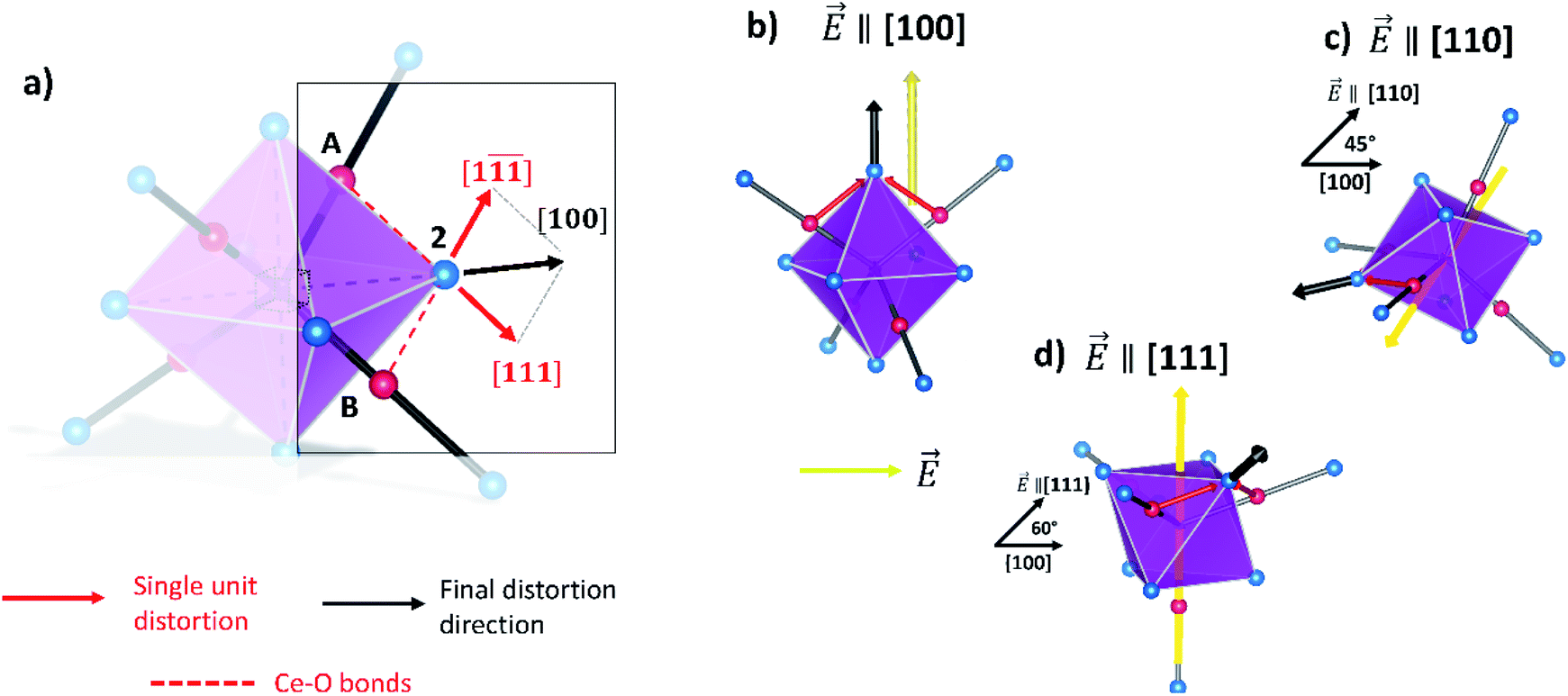 | ||
Fig. 4 Microscopic interpretation of CGO electrostriction in the  neighborhood lattice. (a) 4-Units complex with neighborhood lattice. (a) 4-Units complex with  triplets imposed stress. (b) Preferred direction in the octahedron structure parallel with the electric field along the [100] direction. (c) Preferred direction (black line) compared to induced stress with an electric field (yellow line) along [110] with an angle of 45°. (d) Preferred direction with the electric field parallel to [111] with a 60° angle. triplets imposed stress. (b) Preferred direction in the octahedron structure parallel with the electric field along the [100] direction. (c) Preferred direction (black line) compared to induced stress with an electric field (yellow line) along [110] with an angle of 45°. (d) Preferred direction with the electric field parallel to [111] with a 60° angle. | ||
The M11 values follow the trend expected from the octahedron model. The highest electromechanical performances are found for the CGO(110)/YSZ(110) sample for fields applied along 〈100〉, intermediate performances for 〈110〉 directions in CGO(100)/STO(100) and lower performances for diagonal direction [−211] in CGO(111)/NGO(100). The M12 values are considerably lower than longitudinal coefficients but, considering both in-plane (y) and vertical (z) directions, the performances of the samples consistently follow the trend expected from the model. Table 1 summarizes the results for the longitudinal and the transverse electrostriction coefficients in different crystal directions. Despite having lower M11 compared to that of CGO(110)/YSZ(110), the CGO(100)/STO(100) sample shows an M12 value of about three times higher. In CGO100/STO100 the out-of-plane distortion takes place along [100]z, which allows an easy release of the stress compared to the [110]z direction in CGO110/YSZ110, resulting thus in a more significant electrostriction coefficient. Remarkably, the M11 of the CGO(100)/STO(100) and CGO(111)/NGO (100) samples shows a difference despite having the field applied along directions of the same family: [011] and [0−11] respectively (Fig. 3f and h). We explained this effect by assuming that the weaker transverse effect of CGO(111)/NGO(100) influences the longitudinal performances.
Orientation∥![[E with combining right harpoon above (vector)]](https://www.rsc.org/images/entities/i_char_0045_20d1.gif) |
Longitudinal M11 (m2 V−2) | Orientation⊥ |
Shear M12 (m2 V−2) | |
|---|---|---|---|---|
| a (z and y denote the vertical and lateral orientation of the films, respectively). The values in the brackets are values calculated without subtracting the contribution of the substrates (Fig. S7–S9). b El. conf. 2 (ESI). | ||||
| CGO110/YSZ110 | [001] | 4.93 (9.11) × 10−17 | [110]z/[−1−10]ya | 0.26.10–17 |
| CGO100/STO100 | [011] | 2.22 (2.45) × 10−17 | [100]z/[01−1]y | 0.79.10–17 |
| CGO111/NGO100 | [0−11] | 3.50 × 10⁻¹⁸ | [111]z/[−211]y | 1.9.10–18 |
| CGO111/NGO100b | [−211] | 2.03 × 10⁻¹⁸ | [111]z/[−101]y | — |
| CGO110/YSZ110b | [−223] | <6.72 × 10⁻¹⁹ | [110]z/[−33−4]y | — |
Conclusions
In this work, we fabricate highly coherent CGO thin films with the (100), (110) and (111) orientation. These films are electromechanically tested using a planar electrode geometry in different electric field directions for both longitudinal (M11) and transverse (M12) coefficients. The electrostrictive performances depend on the crystallographic direction of the film, showing a maximum value of M11 = 4.93 × 10⁻¹⁷ m2 V−2 along the 〈100〉 direction, followed by 〈110〉 and then 〈111〉. To support the experimental results, we propose an extension of the current model, based on the octahedron structure of oxygen atoms neighbouring a site. Using such an interpretation, we explain the reason for the performance trend dependent on the crystallographic direction, giving new insight into the microscopic mechanism behind electrostriction in CGO.
Conflicts of interest
There are no conflicts to declare.Acknowledgements
This research was supported by the Danish Council for Independent Research Technology and Production Sciences for the DFF-Research Project 2 (Grant No. 48293) and the BioWings project funded by the European Union's Horizon 2020, Future and Emerging Technologies (FET) programme (Grant No. 801267).References
- V. Esposito and E. Traversa, J. Am. Ceram. Soc., 2008, 91, 1037–1051 CrossRef CAS.
- S. Sanna, V. Esposito, D. Pergolesi, A. Orsini, A. Tebano, S. Licoccia, G. Balestrino and E. Traversa, Adv. Funct. Mater., 2009, 19, 1713–1719 CrossRef CAS.
- C. Sun, H. Li and L. Chen, Energy Environ. Sci., 2012, 5, 8475–8505 RSC.
- P. Jasinski, T. Suzuki and H. U. Anderson, Sens. Actuators, B, 2003, 95, 73–77 CrossRef CAS.
- M. Kuhn, S. R. Bishop, J. L. M. Rupp and H. L. Tuller, Acta Mater., 2013, 61, 4277–4288 CrossRef CAS.
- J. Kas, P. Fornasiero and M. Graziani, Catal. Today, 1999, 50, 285–298 CrossRef.
- N. Yang, Y. Shi, S. Schweiger, E. Strelcov, A. Belianinov, V. Foglietti, P. Orgiani, G. Balestrino, S. V. Kalinin, J. L. M. Rupp and C. Aruta, ACS Appl. Mater. Interfaces, 2016, 8, 14613–14621 CrossRef CAS PubMed.
- A. Younis, D. Chu, X. Lin, J. Yi, F. Dang and S. Li, ACS Appl. Mater. Interfaces, 2013, 5, 2249–2254 CrossRef CAS PubMed.
- S. Schweiger, M. Kubicek, F. Messerschmitt, C. Murer and J. L. M. Rupp, ACS Nano, 2014, 8, 5032–5048 CrossRef CAS PubMed.
- R. Schmitt, J. Spring, R. Korobko and J. L. M. Rupp, ACS Nano, 2017, 11, 8881–8891 CrossRef CAS PubMed.
- N. Pryds and V. Esposito, J. Electroceram., 2017, 38, 1–23 CrossRef CAS.
- K. Rodrigo, S. Heiroth, M. Lundberg, N. Bonanos, K. Mohan Kant, N. Pryds, L. Theil Kuhn, V. Esposito, S. Linderoth, J. Schou and T. Lippert, Appl. Phys. A: Mater. Sci. Process., 2010, 101, 601–607 CrossRef CAS.
- K. M. Kant, V. Esposito and N. Pryds, Appl. Phys. Lett., 2010, 97, 5–8 CrossRef.
- M. Melchionna and P. Fornasiero, Mater. Today, 2014, 17, 349–357 CrossRef CAS.
- S. Ackermann and A. Steinfeld, J. Phys. Chem., 2014, 5216–5225 CAS.
- I. Kosacki, T. Suzuki, V. Petrovsky and H. U. Anderson, Solid State Ionics, 2000, 136–137, 1225–1233 CrossRef CAS.
- K. Mohan Kant, V. Esposito and N. Pryds, Appl. Phys. Lett., 2012, 100, 033105 CrossRef.
- S. Wang, T. Kobayashi, M. Dokiya and T. Hashimoto, J. Electrochem. Soc., 2000, 147, 3606 CrossRef CAS.
- G. Baure, R. M. Kasse, N. G. Rudawski and J. C. Nino, Phys. Chem. Chem. Phys., 2015, 17, 12259–12264 RSC.
- T. S. Stefanik and H. L. Tuller, J. Electroceram., 2004, 13, 799–803 CrossRef CAS.
- S. R. Bishop, T. S. Stefanik and H. L. Tuller, Phys. Chem. Chem. Phys., 2011, 13, 10165–10173 RSC.
- R. Korobko, A. Patlolla, A. Kossoy, E. Wachtel, H. L. Tuller, A. I. Frenkel and I. Lubomirsky, Adv. Mater., 2012, 24, 5857–5861 CrossRef CAS PubMed.
- S. Santucci, H. Zhang, S. Sanna, N. Pryds and V. Esposito, APL Mater., 2019, 7, 071104 CrossRef.
- R. Korobko, E. Wachtel and I. Lubomirsky, Sens. Actuators, A, 2013, 201, 73–78 CrossRef CAS.
- A. D. Ushakov, N. Yavo, E. Mishuk, I. Lubomirsky, V. Y. Shur and A. L. Kholkin, KnE Mater. Sci., 2016, 1, 177 CrossRef.
- M. Hadad, H. Ashraf, G. Mohanty, C. Sandu and P. Muralt, Acta Mater., 2016, 118, 1–7 CrossRef CAS.
- A. Kabir, S. Santucci, N. Van Nong, M. Varenik, I. Lubomirsky, R. Nigon, P. Muralt and V. Esposito, Acta Mater., 2019, 174, 53–60 CrossRef CAS.
- N. Yavo, O. Yeheskel, E. Wachtel, D. Ehre, A. I. Frenkel and I. Lubomirsky, Acta Mater., 2018, 144, 411–418 CrossRef CAS.
- E. Mishuk, E. Makagon, E. Wachtel, S. R. Cohen, R. Popovitz-Biro and I. Lubomirsky, Sens. Actuators, A, 2017, 264, 333–340 CrossRef CAS.
- A. D. Ushakov, E. Mishuk, E. Makagon, D. O. Alikin, A. A. Esin, I. S. Baturin, A. Tselev, V. Y. Shur, I. Lubomirsky and A. L. Kholkin, Appl. Phys. Lett., 2017, 110, 142902 CrossRef.
- E. Mishuk, A. D. Ushakov, S. R. Cohen, V. Y. Shur, A. L. Kholkin and I. Lubomirsky, Solid State Ionics, 2018, 327, 47–51 CrossRef CAS.
- R. E. N. V. Sundar, J.-F. Li and D. Viehland, Mater. Res. Bull., 1996, 31, 555–563 CrossRef.
- R. E. Newnham, V. Sundar, R. Yimnirun, J. Su and Q. M. Zhang, J. Phys. Chem. B, 1997, 101, 10141–10150 CrossRef CAS.
- N. Yavo, A. D. Smith, O. Yeheskel, S. Cohen, R. Korobko, E. Wachtel, P. R. Slater and I. Lubomirsky, Adv. Funct. Mater., 2016, 26, 1138–1142 CrossRef CAS.
- S. Kim and J. Maier, J. Electrochem. Soc., 2002, 149, J73 CrossRef CAS.
- R. Korobko, A. Lerner, Y. Li, E. Wachtel, A. I. Frenkel and I. Lubomirsky, Appl. Phys. Lett., 2015, 106, 042904 CrossRef.
- Y. Li, O. Kraynis, J. Kas, T. C. Weng, D. Sokaras, R. Zacharowicz, I. Lubomirsky and A. I. Frenkel, AIP Adv., 2016, 6, 055320 CrossRef.
- L. Sun, D. Marrocchelli and B. Yildiz, Nat. Commun., 2015, 6, 1–10 Search PubMed.
- Y. Lei, Y. Ito, N. D. Browning and T. J. Mazanec, J. Am. Ceram. Soc., 2002, 85, 2359–2363 CrossRef CAS.
- S. Kim, P. Jain, H. J. Avila-Paredes, A. Thron, K. Van Benthem and S. Sen, J. Mater. Chem., 2010, 20, 3855–3858 RSC.
- Y. L. Kuo, C. Lee, Y. S. Chen and H. Liang, Solid State Ionics, 2009, 180, 1421–1428 CrossRef CAS.
- H. J. Avila-Paredes, K. Choi, C. T. Chen and S. Kim, J. Mater. Chem., 2009, 19, 4837–4842 RSC.
- A. Infortuna, A. S. Harvey and L. J. Gauckler, Adv. Funct. Mater., 2008, 18, 127–135 CrossRef CAS.
- A. Kossoy, Q. Wang, R. Korobko, V. Grover, Y. Feldman, E. Wachtel, A. K. Tyagi, A. I. Frenkel and I. Lubomirsky, Phys. Rev. B: Condens. Matter Mater. Phys., 2013, 87, 054101 CrossRef.
- K. Uchino, S. Nomura, L. E. Cross, R. E. Newnham and S. J. Jang, J. Mater. Sci., 1981, 16, 569–578 CrossRef CAS.
- F. Li, L. Jin, Z. Xu and S. Zhang, Appl. Phys. Rev., 2014, 1, 011103 Search PubMed.
- F. Li, L. Jin, Z. Xu, D. Wang and S. Zhang, Appl. Phys. Lett., 2013, 102, 152910 CrossRef.
- S. Sanna, V. Esposito, A. Tebano, S. Licoccia, E. Traversa and G. Balestrino, Small, 2010, 6, 1863–1867 CrossRef CAS PubMed.
- R. Sinclair, S. C. Lee, Y. Shi and W. C. Chueh, Ultramicroscopy, 2017, 175, 25–35 CrossRef CAS PubMed.
- L. Chen, C. L. Chen, D. X. Huang, Y. Lin, X. Chen and A. J. Jacobson, Solid State Ionics, 2004, 175, 103–106 CrossRef CAS.
- N. Yang, P. Orgiani, E. Di Bartolomeo, V. Foglietti, P. Torelli, A. V. Ievlev, G. Rossi, S. Licoccia, G. Balestrino, S. V. Kalinin and C. Aruta, J. Phys. Chem. C, 2017, 121, 8841–8849 CrossRef CAS.
- M. Mathews, E. P. Houwman, H. Boschker, G. Rijnders and D. H. A. Blank, J. Appl. Phys., 2010, 107, 013904 CrossRef.
- Y. Shi, S. C. Lee, M. Monti, C. Wang, Z. A. Feng, W. D. Nix, M. F. Toney, R. Sinclair and W. C. Chueh, ACS Nano, 2016, 10, 9938–9947 CrossRef CAS PubMed.
- A. Selçuk and A. Atkinson, J. Eur. Ceram. Soc., 1996, 17, 1523–1532 CrossRef.
- R. Korobko, C. T. Chen, S. Kim, S. R. Cohen, E. Wachtel, N. Yavo and I. Lubomirsky, Scr. Mater., 2012, 66, 155–158 CrossRef CAS.
- J. C. Goldsby, J. Ceram., 2012, 2013, 1–4 Search PubMed.
- M. Fujikane, D. Setoyama, S. Nagao, R. Nowak and S. Yamanaka, J. Alloys Compd., 2007, 431, 250–255 CrossRef CAS.
- L. Kurpaska, M. Frelek-Kozak, K. Nowakowska-Langier, M. Lesniak, J. Jasinski and J. Jagielski, Nucl. Instrum. Methods Phys. Res., Sect. B, 2017, 409, 81–85 CrossRef CAS.
Footnote |
| † Electronic supplementary information (ESI) available. See DOI: 10.1039/d0ta05500j |
| This journal is © The Royal Society of Chemistry 2020 |