
 Open Access Article
 This Open Access Article is licensed under a
 Creative Commons Attribution 3.0 Unported Licence
Humidity-robust scalable metal halide perovskite film deposition for photovoltaic applications†
Carlo Andrea Riccardo
Perini‡
 ab,
Anil
Reddy Pininti‡
ab,
Samuele
Martani
ab,
Peter
Topolovsek
a,
Andrea
Perego
a,
Daniele
Cortecchia
a,
Annamaria
Petrozza
a and
Mario
Caironi
*a
ab,
Anil
Reddy Pininti‡
ab,
Samuele
Martani
ab,
Peter
Topolovsek
a,
Andrea
Perego
a,
Daniele
Cortecchia
a,
Annamaria
Petrozza
a and
Mario
Caironi
*a
aCenter for Nano Science and Technology @ PoliMi, Istituto Italiano di Tecnologia, Via G. Pascoli 70/3, 20133, Milan, Italy. E-mail: mario.caironi@iit.it
bPhysics Department, Politecnico di Milano, Piazza L. da Vinci, 32, 20133 Milano, Italy
First published on 25th November 2020
Abstract
Organic–inorganic perovskite photovoltaics have now achieved power conversion efficiencies at par with silicon devices on a lab-scale. To enable industrial application of the technology, developing a perovskite deposition route compatible with scalable, large-area deposition methods, which exploits safer processing solvents and is robust to variations of the processing parameters, particularly humidity, is highly demanded. To satisfy such constraints altogether, here we introduce a lead iodide–hydroiodic acid–water precursor (PbI2–HI–H2O) that enables the scalable deposition of methylammonium lead triiodide (MAPbI3) films from a safer solvent (acetonitrile – ACN) in a wide range of high moisture levels, spanning from 50 to 80% relative humidity. When exposed to a methylamine (MA) gas flow the PbI2–HI–H2O precursor readily converts to specular perovskite films. If heated, the PbI2–HI–H2O film can be easily reverted to PbI2, further enabling the implementation of two step deposition methods. Our process was tested in an inverted solar cell configuration achieving stabilized power conversion efficiencies of 14% with minimal annealing requirements. Our findings demonstrate an appealing route for a large-area compatible manufacturing of hybrid perovskite photovoltaics in air, at high moisture levels, based on solvents of reduced hazard.
Introduction
In less than a decade, organic–inorganic hybrid perovskites have risen to the foreground in photovoltaics research, combining high performances with simple processing. Power conversion efficiencies above 25% have been demonstrated by carefully optimizing the quality of the active thin films and their interfaces within a device.1,2 The Earth abundance of perovskite precursors and their processability from solution promise reduced fabrication costs without compromising excellent device performances. Devices can in principle be deposited on flexible substrates at low temperature, exploiting high throughput approaches.3–6 To harvest such benefits, low temperature fabrication routes compatible with large-area coating, stable in the ambient atmosphere and based on non-hazardous solvents, are required. Significant efforts have been committed to upscale metal halide perovskite deposition, particularly in inverted device structures, yet only limited efforts have been addressed to the latter two desired aspects.7,8 High boiling point, hazardous solvents as dimethylformamide (DMF), dimethyl sulfoxide (DMSO), and γ-butyrolactone (GBL) are typically employed for perovskite deposition, despite various attempts made towards their replacement.9–14 Their use raises concerns not only in relation to their health hazard, but also owing to the related difficulty in obtaining uniform films under humid air conditions.15–17 Uniform perovskite deposition in the ambient atmosphere can be pursued by exploiting hydrophobic compounds or inducing an increased nucleation rate, to hamper the rearrangement of precursors and their interaction with moisture and water.18 A clear example is the rapid recrystallization that follows a methylamine (MA) gas induced solvation of methylammonium lead triiodide (MAPbI3), which has been demonstrated to be effective for healing defective perovskite films in air, deposited by conventional routes.19,20 At present, a sole example, based on an acetonitrile (ACN)–CH3NH2 (methylamine) blend, succeeded in demonstrating contemporarily a scalable perovskite deposition in humid air from a solvent of reduced hazard.21–23 However, such a process has been proven to work only at low relative humidity (RH, <30%), imposing constraints on the deposition environment.18 A low-temperature fabrication route simultaneously fulfilling the requirements of scalability, a broad operational window at different RH values and based on solvents of limited hazard is still missing.Here we demonstrate a novel perovskite precursor formulation that enables MAPbI3 deposition from acetonitrile within a broad RH range, from 50 to 80%. Simply adding stoichiometric hydroiodic acid (HI) to lead iodide (PbI2) permits its solvation in ACN. The acid serves the dual purpose of triggering the precursor formation, later referenced as PbI2–HI–H2O, and preserving the iodine balance during the subsequent conversion to MAPbI3. The perovskite is obtained by exposing the PbI2–HI–H2O film to methylamine gas. A rapid crystallization is prompted, leading to the formation of specular perovskite films regardless of the high RH of the environment. We selected the so-called inverted solar cell architecture, i.e. ITO/PEDOT:PSS (hole extraction layer)/MAPbI3/PC60BM/BCP (electron extraction layer)/Ag, to test the photovoltaic properties of our films as it facilitates fabrication on plastic foil, owing to the low temperature solution-based deposition of the charge transporting interlayers. The obtained devices achieve a stabilized power conversion efficiency (PCE) of up to 14% on a 0.0935 cm2 active area. Notably, a short 5 min annealing time of the converted film is sufficient to achieve the optimal solar cell performance. Importantly, the stability of the ACN-processed film is comparable with that of MAPbI3 deposited in a nitrogen atmosphere via conventional routes. Furthermore, we demonstrate the compatibility of our approach with large area deposition techniques such as blade coating. The proposed fabrication route offers several advantages as it enables PbI2 solvation in a less hazardous compound, it is reliable over a broad relative humidity range, and it provides an increased flexibility in processing from ACN, decoupling PbI2 (precursor) deposition and perovskite formation.
Results and discussion
Perovskite film formation
The key observation of our precursor route is that ACN solvation power of PbI2 can be significantly enhanced via addition of stoichiometric HI to the system, enabling preparation of up to 2 M solutions characterized by a clear, light-red colour (Fig. S1†). Deposition in the ambient atmosphere of the PbI2 solution, at a RH within the 50 to 80% range, leads to the formation of a pale-white film (its absorption profile is shown in Fig. S2†). The X-ray diffractogram (XRD) of the material, presented in Fig. 1a (see Fig. S3† for magnification), indicates the formation of a crystalline compound that has a main diffraction peak at 8.9° and is clearly distinct both from PbI2 (12.7°) and from HPbI3 (11.65°, obtained via deposition from DMF) fingerprints.24–26 It has been suggested that the compound reported as HPbI3 might instead be (CH3)2NH2PbI3: a by-product formed upon DMF degradation by exposure to an acidic environment.27 We therefore investigated the possibility of solvent involvement in the formation of our precursor, and we performed liquid-state proton nuclear magnetic resonance (1H NMR) measurements. The spectrum of the film, dissolved in deuterated DMSO, exhibits a single peak with an intermediate chemical shift between those of water and of an acidic HI solution (Fig. 1b). It markedly differs from the ones of ACN and of its degradation products (i.e. acetamide or acetic acid – Fig. S4a†). Consequently, the presence of either ACN or of solvent by-products can be excluded, and the peak can be ascribed to water, with an offset position due to the presence of a weakly acidic environment (Fig. S4b and c†).28 To corroborate such a hypothesis, we exposed a PbI2–HI–H2O film to low RH (<50%), low vacuum levels (glovebox antechamber, −1 bar) or heat (100 °C, 10 s), and followed the evolution of its XRD spectrum. Under all such circumstances the film reverts to PbI2, as highlighted by the appearance of the characteristic peak at 12.7° (Fig. S5†). | ||
| Fig. 1 (a) XRD spectra of the PbI2–HI–H2O film processed from ACN (red), of PbI2 (green) from DMF and of PbI2–HI deposited from DMF (HPbI3-blue). (b) 1H NMR spectra of the PbI2–HI–H2O film dissolved in deuterated DMSO (red), water (blue), HI solution (orange) and ACN (purple). The peak visible at 2.50 ppm is due to the residual proton signal (DMSO-d5) in DMSO-d6. | ||
We use this PbI2–HI–H2O film as a starting phase for conversion to CH3NH3PbI3 through exposure to MA gas. We adopt a MA laminar flow, which enables us to achieve controlled conversion to high quality films. Upon contact with methylamine, a series of reactions is triggered. Perovskite formation is manifest with an immediate switch of the film to a light brown colour (i), which then turns transparent because of MA solvation (ii).19 Upon interruption of the MA flow, the film swiftly reverts to a brown perovskite phase (iii), a transition we attribute to perovskite recrystallization induced by MA desorption. The so deposited perovskite will be henceforth labelled MA-PVK. The overall process requires less than 10 s for completion. Perturbations of the MA laminar flow during conversion or drops in the MA pressure in the glass flask used for flushing can result in a greyish and rough film. Interestingly, in these cases MA flushing can be repeated, resulting in improved smoothness and reflectivity when the laminar flow is stabilised and the MA partial pressure is restored. The scheme of the proposed reaction is depicted in Fig. 2, together with images relative to the different steps of conversion, and with a sketch of the setup used to perform the flushing. ESI Video 1† provides an outlook of the process. The following sequence summarizes the proposed reaction pathway:
| HI + PbI2 + H2O ⇌ PbI2–HI–H2O, | (1.1) |
| PbI2–HI–H2O + CH3NH2(g) → CH3NH3PbI3(s) + H2O(g), | (1.2) |
| CH3NH3PbI3(s) + xCH3NH2(g) ⇌ CH3NH3PbI3·xCH3NH2. | (1.3) |
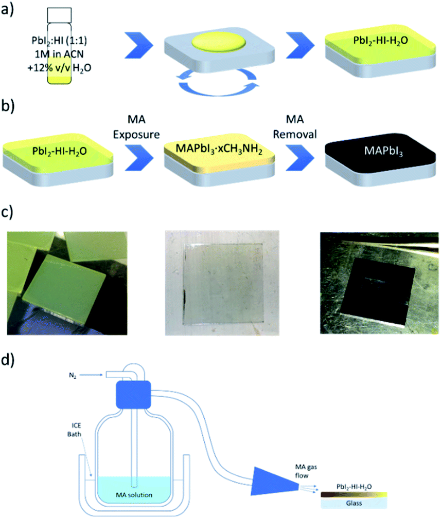 | ||
| Fig. 2 (a) Pb-precursor solution and film formation upon deposition in a moist environment (RH > 50%). (b) Conversion of the film to MAPbI3 upon exposure to MA gas. MA is first protonated leading to perovskite formation; the gas excess then contributes to film solvation. Upon removal of the methylamine flow, excess MA is desorbed from the film. (c) Photographic images of the films from left to right: PbI2–HI–H2O, solvated PVK film, smooth PVK sample reflecting the image of tweezers. (d) Schematic of the setup used to perform the MA side-flushing on films. | ||
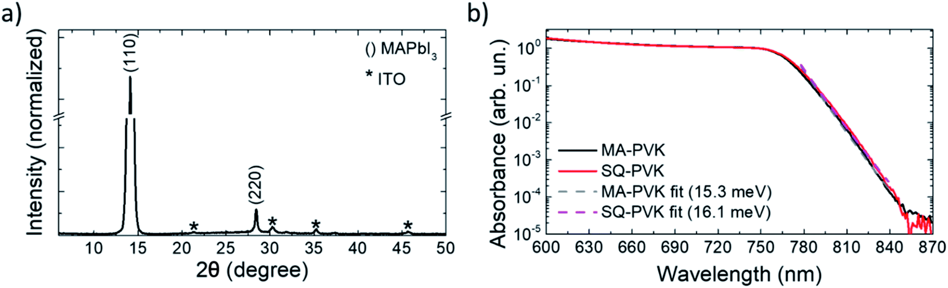
After deposition, the PbI2–HI–H2O film is in equilibrium with its precursors. Low moisture levels (<50% RH) can move the equilibrium towards the precursors, resulting in release of H2O(g) and HI(g) with formation of PbI2(s). At higher relative humidity, the film retains its composition and can be converted to MAPbI3 upon exposure to MA as indicated in (1.2), with the release of the excess H2O molecules. The solvation of the film immediately follows MAPbI3 formation and is induced by the gas excess (1.3).29 As the MA flow is interrupted, the equilibrium of (1.3) is moved towards the reactants, inducing a rapid crystallization back to the perovskite. The XRD pattern of the MA-PVK layer, presented in Fig. 3a, exhibits reflections typical of the tetragonal perovskite phase, belonging to the I4/mcm space group.29 The main spectral features are visible at 14.1° and 28.4°, related to the (110) and (220) crystalline planes, suggesting a preferred orientation along the (110) direction. The higher order (220) reflection is significantly attenuated, a possible marker of disorder in the lattice, or of a reduced extension of crystalline domains. Previous reports evidenced an increased electronic disorder in metal halide perovskite films post-processed with MA, reflected by a broadening in the Urbach tail of the absorption.30 We thus performed photothermal deflection spectroscopy (PDS) measurements to compare the Urbach energies of MA-PVK with those of a conventional solvent quenched MAPbI3 film (sq-PVK).30 We observed slopes of 16.1 meV for sq-PVK and of 15.3 meV for MA-PVK, indicating similar and even slightly lower contribution of band tail states for the perovskite converted with MA from the PbI2–HI–H2O precursor (Fig. 3b).
 | ||
| Fig. 3 (a) XRD pattern of the MA-treated perovskite film. The CH3NH3PbI3 related peaks are indexed in parentheses, whereas the substrate related peaks are marked with a * (Fig. S10†). (b) PDS spectra of solvent quenched MAPbI3 and of MA-PVK. Fits to the experimental data are also shown in the figure. | ||
Solar cell fabrication and characterization
We exploited a newly developed absorber deposition strategy to fabricate a low-temperature processed inverted solar cell, which is compatible with flexible substrates.31 We adopted only solution processed interlayers: poly(3,4-ethylenedioxythiophene):polystyrene sulfonate (PEDOT:PSS) as a hole transporting layer (HTL), and a phenyl-C61-butyric acid methyl ester (PC60BM)/bathocuproine (BCP) stack as an electron transporting layer. Indium tin oxide (ITO) and silver (Ag) were employed as electrodes (Fig. 4a). The whole fabrication flow is performed at temperatures below 100 °C, with short annealing times of less than 10 min per layer. Fig. 4b presents a cross sectional image of the complete device processed at 65% RH. We observe a 550 nm thick active layer, with grains as thick as the film and having micron-scale lateral sizes. It was proposed that the boundaries limiting charge carrier transport are those visible from the SEM images.32 According to such consideration, grains crossing the whole film thickness would result in efficient charge collection. A top-view SEM image of the film is presented in Fig. S8.†Fig. 4c presents the current–voltage characteristic curve of our champion device. It demonstrates a short circuit current (Jsc) of 18.3 mA cm−2, combined with an open circuit voltage (Voc) of 0.94 V and a fill factor (FF) of 77% in reverse scan. Together, these parameters result in a 13.3% PCE in reverse scan (statistical distribution is reported in Fig. 4f). 300 s of maximum power point tracking contribute to a stabilized PCE of 14% (Fig. 4d). The external quantum efficiency (EQE) spectrum is almost flat (Fig. S9†). A slight loss is observed at lower wavelengths, to be ascribed to recombination at the PEDOT:PSS interface.33 The integrated Jsc, computed from the EQE spectrum, amounts to 18.1 mA cm−2, and well matches with the short circuit current measured in the current–voltage scan. 5 min of annealing of the perovskite layer at 100 °C are sufficient to maximise the device performances. Longer timings induce a slight decrease in PCEs and the appearance of PbI2 in the films, as highlighted by both the XRD and SEM images (Fig. S10†). It is known that thickness variations can induce performance fluctuations owing to increased recombination and poorer charge transport. However, it has been shown that perovskite films can be used even in thick films without loss in the efficiency of solar cells, provided that they are of high optoelectronic quality.34 For MA-PVK devices, the concentration of the precursor solution can be changed from 1 to 1.2 M with negligible impact on the PCE values, as shown in Fig. S11,† an advantageous feature towards high throughput fabrication. The deposition of MA-PVK proves effective over a broad range of high RH values, between 50 and 80%, where the solar cells provide average PCEs ranging from 9 to 12% (Fig. 4e). At RH below 50% the PCE abruptly decreases, owing to a reduced short circuit current density approaching 0 mA cm−2 for the devices processed in a glovebox (0% RH). Complete photovoltaic parameters are reported in Fig. S12.† The drop in currents is associated with a significant decrease in the crystallinity of MA-PVK and with the appearance of a (001) PbI2 peak at 12.7°, as shown in Fig. S13.† The presence of PbI2 is consistent with the degradation of the PbI2–HI–H2O precursor in dry environments discussed in the previous section and presented in Fig. S5.† The lower PCE at low RH is thus attributed to the lack of crystallinity of the film and to the presence of a lead iodide excess, both contributing to limiting charge collection. The characterization of the photovoltaic performances of MA-PVK based solar cells is completed by evaluating the device stability. The ‘shelf life’ is a widely used stability protocol for inverted device structures using PEDOT:PSS as the hole extraction layer, as shown in the literature survey presented in Table S1.† We thus present here the ‘shelf Life’ of solar cells processed including a MA-PVK layer. MA-PVK based solar cells experience negligible performance variations over >1400 h, similarly to our reference sample processed in a glovebox from DMF (Fig. S14†). Such a lifetime is longer than most of those reported for similar architectures and perovskite layers in the literature, as can be seen in Table S2,† confirming the quality of the perovskite film processed with our route.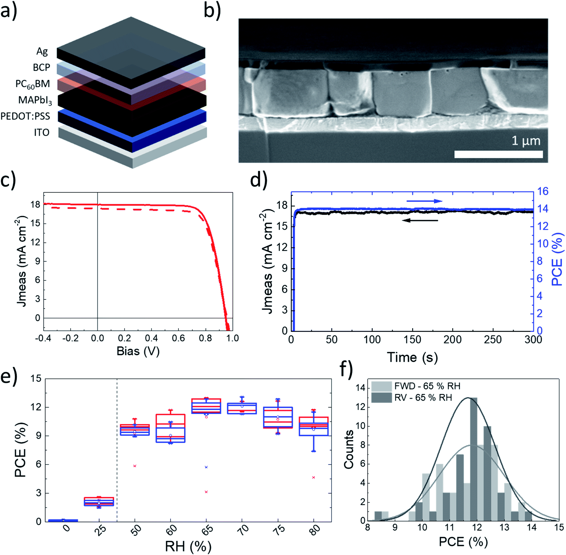 | ||
| Fig. 4 (a) Solar cell device structure. (b) SEM cross sectional image of the complete device. (c) J/V scans in the forward (dashed) and reverse (solid) direction of the champion device. (d) Maximum power point tracking stabilization of the device. (e) RH dependence of device efficiency. Below 50% the PbI2–HI–H2O starts decomposing into PbI2, resulting in an efficiency drop. The vertical dashed lines separate humidity levels that are too low for the proposed processing method (left side) from those which are compatible with it (right side). (f) Widened performance distribution for the devices processed at 65% RH with 5 min annealing. | ||
To provide the first assessment of the scalability of the proposed fabrication route, we printed, via blade coating, thin films on 7.5 cm × 2.5 cm glass slides (Fig. S15†). For simplicity, we adopted an identical device architecture and perovskite formulation, without re-optimization. The layer uniformly covers the glass substrate. The solar cells are fabricated on smaller glass/ITO substrates with the same method. Uniform performances are obtained over an area > 3 cm2, as shown in Fig. S16.† The best performing pixel shows a stabilized PCE of 7.6% (Fig. S17†) on an active area of 0.0935 cm2. Such efficiency is promising, given the simplicity of this initial attempt, and confirms the compatibility of the proposed process with simple, large-area coating and scalable techniques.
Conclusions
We developed a novel processing route for the deposition of hybrid perovskite films in air for photovoltaic applications. The method enables deposition of high-quality films in a wide range of high moisture levels and it is compatible with scalable deposition techniques such as blade-coating. Importantly, by engineering the formation of a PbI2–HI–H2O complex in the precursor solution, we are able to perform our deposition from acetonitrile, a solvent of moderate toxicity with respect to solvents mostly used in this field. Minimal perovskite film annealing times, below 5 minutes, still enable optimal performances when the absorber is adopted in solar cells, making the process attractive for high throughput applications. A stabilized PCE of 14% is achieved for the champion device, while active layers fabricated from blade-coating show compatibility with large-area processing. Despite not achieving record PCE values, the solvation approach we propose demonstrates a powerful alternative path towards the fabrication of metal halide perovskite solar cells with greener solvent systems, favouring the future development of large-scale industrial processes.Experimental
Thin film fabrication
Various molarities of PbI2![[thin space (1/6-em)]](https://www.rsc.org/images/entities/char_2009.gif) :HI (1:1) in ACN were prepared, at least 4 hours before the start of the experiment, by adding to 1 ml of ACN the required volume of HI solution (Sigma-Aldrich, 57 wt% in H2O, distilled, stabilized, 99.95%), and weight of PbI2 (TCI, 99.99%, trace metals basis). The solutions were left stirring until complete dissolution (for the 1 M case 132 μl of HI and 461 mg of PbI2 were used).
:HI (1:1) in ACN were prepared, at least 4 hours before the start of the experiment, by adding to 1 ml of ACN the required volume of HI solution (Sigma-Aldrich, 57 wt% in H2O, distilled, stabilized, 99.95%), and weight of PbI2 (TCI, 99.99%, trace metals basis). The solutions were left stirring until complete dissolution (for the 1 M case 132 μl of HI and 461 mg of PbI2 were used).
Indium doped tin oxide (ITO) glass substrates were patterned by reaction with zinc powder and HCl and subsequently cleaned by sonication in Hellmanex (Hellmanex III – Sigma-Aldrich, 2% v/v in water), water (×2), isopropanol (IPA), acetone and IPA for 10 min each. Oxygen plasma cleaning (6 min) was performed immediately before spin coating PEDOT:PSS (Clevios P VP Al4083, Heraeus). The HTL was filtered with a 0.22 μm PVDF filter, deposited at 4000 rpm for 40 s, and annealed at 100 °C for 10 min. The PbI2–HI (ACN) solution was spin cast at 6000 rpm, for 20 s in air, at different moisture levels, and then exposed within 10 s from deposition to an MA gas flow for 2 s. The substrates were then annealed for 10 s, at 100 °C, and exposed a second time after substrate cooling, to the MA gas flow (5 s). After the second (5 min, 100 °C) annealing step, the substrates were transferred to a nitrogen glovebox, for the deposition of the electron selective layer. A PC60BM solution (40 mg ml−1 in chlorobenzene, CB) was filtered with a 0.22 μm PTFE filter and spin cast at 1000 rpm for 40 s. Following a 40 s, 60 °C solvent removal step, a bathocuproine solution (BCP, 2 mg ml−1 in IPA, filtered with PTFE 0.22 μm) was spin cast at 5000 rpm for 40 s. The devices were completed with evaporation of a 75 nm silver electrode. Fabrication was performed up to the perovskite layer deposition for top-view SEM and XRD characterization. For the PDS measurements, the sole MA-PVK film was deposited on quartz substrates. For the solvent quenched perovskite a previously reported recipe was used.35 Solar cells with a blade-coated active layer were prepared by dropping a 1 M precursor solution on the HTL, and by swiping it by hand with a microscope slide. Two microscope glasses were placed at the sample sides to act as spacers between the blade and the sample surface, similarly to the configuration reported by Deng et al.36 After waiting for a few seconds to permit the drying of the film, the substrate was subjected to a MA flow. The as formed perovskite layer was then annealed for 10 minutes at 100 °C. The devices were completed as in the case of the spin cast samples.
Device characterization
Current density/voltage (J/V) characteristics were recorded in air on non-encapsulated devices, performing forward and reverse bias sweeps under illumination at a scan speed of 0.1 V s−1, without light or bias pre-conditioning.37 An AM 1.5 AAA class Newport solar simulator, calibrated with an NREL certified reference diode (0.99 spectral mismatch factor), was used for illumination. The devices were masked for accurate definition of the active area (0.0935 cm2). Data collection was performed via a computer-controlled Keithley 2400 source measure unit. Stabilized performances were recorded using maximum power point tracking software, for a time span of 300 s. External quantum efficiency was recorded with a home-built setup, composed of a tungsten–halogen lamp and of an Oriel Apex monochromator illuminator, which were coupled with a Keithley 2300 and calibrated with a Newport silicon photodiode (UV-818).Stability measurements were performed adopting the shelf life as performance indicator. The devices were stored in a glovebox and exposed to air only to record their J/V characteristics. No encapsulation was used.
Material characterization
X-ray diffraction (XRD) patterns were acquired using a BRUKER D8 ADVANCE diffractometer equipped with a Cu Kα1 (λ = 1.544060 Å) anode, operating at 40 kV and 40 mA, in a Bragg–Brentano geometry. Spectral acquisition was performed using 0.05° angular steps with 1 s integration.Scanning electron microscope (SEM) images were taken with a Zeiss Supra 40 A at 1 kV acceleration for cross sections. A Jeol JSM-6010LV at 10 kV acceleration was used to acquire top views.
The proton nuclear magnetic resonance (1H NMR) spectra of organic compounds and the chemical shifts of water as a function of pH were recorded in a DMSO-d6 solution with a Bruker ARX 400 (400 MHz) NMR spectrometer. Chemical shift values (ppm) were referenced against residual protic solvent peaks.
Photothermal deflection spectroscopy (PDS) was performed on the samples immersed in a sealed cuvette, filled with an inert liquid (tetradecafluorohexane – 99%, Sigma Aldrich) having a strong temperature dependence of the refractive index. A supercontinuum laser (SuperK Extreme from NKT Photonics) was used to excite the samples from the film side. The monochromatic light was set perpendicular to the film surface and the wavelength was swept, by exploiting a CM110-Monochromator from Spectral Products. A second laser beam (HeNe, JDSU) was fixed parallel to the sample, in close proximity. Its deflection, consequence of the film excitation, was measured with a quadrant detector (PDQ80A, Thorlabs) coupled with a lock-in amplifier (SR830, Stanford Research Systems). Urbach energies were estimated by fitting the exponential tail that follows the band edge with the empirical relation:
| α = α0e(hν−E0)/EU |
Conflicts of interest
There are no conflicts to declare.Acknowledgements
We would like to acknowledge Roberto Sorrentino, Marina Gandini and Min Kim for the fruitful exchange of ideas and the help provided towards the development of this work. A. R. P. and M. C. acknowledge funding from the European Research Council (ERC) under the European Union's Horizon 2020 research and innovation program “HEROIC”, Grant Agreement 638059.Notes and references
- NREL – Efficiency Chart, https://www.nrel.gov/pv/assets/pdfs/pv-efficiency-chart.20181221.pdf.
- K. Liu, Y. Y. Jiang, Y. Y. Jiang, Y. Guo, Y. Liu and E. Nakamura, J. Am. Chem. Soc., 2019, 141, 1406–1414 CrossRef CAS.
- J. M. Ball and A. Petrozza, Nat. Energy, 2016, 1, 16149 CrossRef CAS.
- H. Zeng, Y. Dong, Y. Zou, J. Song and X. Song, J. Mater. Chem. C, 2017, 5, 11369–11394 RSC.
- L. Meng, J. You and Y. Yang, Nat. Commun., 2018, 9, 5265 CrossRef CAS.
- H. J. Snaith, Nat. Mater., 2018, 17, 372–376 CrossRef CAS.
- Z. Yang, S. Zhang, L. Li and W. Chen, J. Materiomics, 2017, 3, 231–244 CrossRef.
- Z. Li, T. R. Klein, D. H. Kim, M. Yang, J. J. Berry, M. F. A. M. van Hest and K. Zhu, Nat. Rev. Mater., 2018, 3, 18017 CrossRef CAS.
- T. H. Kim and S. G. Kim, Saf. Health Work, 2011, 2, 97–104 CrossRef CAS.
- K. L. Gardner, J. G. Tait, T. Merckx, W. Qiu, U. W. Paetzold, L. Kootstra, M. Jaysankar, R. Gehlhaar, D. Cheyns, P. Heremans and J. Poortmans, Adv. Energy Mater., 2016, 6, 1–8 Search PubMed.
- D. M. Wood, A. D. Brailsford and P. I. Dargan, Drug Test. Anal., 2011, 3, 417–425 CrossRef CAS.
- T.-Y. Hsieh, T.-C. Wei, K.-L. Wu, M. Ikegami and T. Miyasaka, Chem. Commun., 2015, 51, 13294–13297 RSC.
- K. Sveinbjörnsson, N. K. Kyi Thein, Z. Saki, S. Svanström, W. Yang, U. B. Cappel, H. Rensmo, G. Boschloo, K. Aitola and E. M. J. Johansson, Sustainable Energy Fuels, 2018, 606–615 RSC.
- J. Wang, F. Di Giacomo, J. Brüls, H. Gorter, I. Katsouras, P. Groen, R. A. J. Janssen, R. Andriessen and Y. Galagan, Sol. RRL, 2017, 1700091 CrossRef.
- Y. Cheng, X. Xu, Y. Xie, H.-W. Li, J. Qing, C. Ma, C.-S. Lee, F. So and S.-W. Tsang, Sol. RRL, 2017, 1700097 CrossRef.
- G. E. Eperon, S. N. Habisreutinger, T. Leijtens, B. J. Bruijnaers, J. J. Van Franeker, W. Dane, S. Pathak, R. J. Sutton, G. Grancini, D. S. Ginger, R. A. J. Janssen, A. Petrozza and H. J. Snaith, ACS Nano, 2015, 9380–9393 CrossRef CAS.
- K. Huang, H. Li, C. Zhang, Y. Gao, T. Liu, J. Zhang, Y. Gao, Y. Peng, L. Ding and J. Yang, Sol. RRL, 2019, 1800318 CrossRef.
- Y. Cheng, F. So and S. W. Tsang, Mater. Horizons, 2019, 6, 1611–1624 RSC.
- S. R. Raga, Y. Jiang, L. K. Ono and Y. Qi, Energy Technol., 2017, 1750–1761 CrossRef CAS.
- K. Huang, C. Wang, C. Zhang, S. Tong, H. Li, B. Liu, Y. Y. Gao, Y. Dong, Y. Y. Gao, Y. Peng and J. Yang, Org. Electron., 2018, 55, 140–145 CrossRef CAS.
- N. K. Noel, S. N. Habisreutinger, B. Wenger, M. T. Klug, M. T. Hörantner, M. B. Johnston, R. J. Nicholas, D. T. Moore and H. J. Snaith, Energy Environ. Sci., 2017, 10, 145–152 RSC.
- B. Dou, J. B. Whitaker, K. Bruening, D. T. Moore, L. M. Wheeler, J. Ryter, N. J. Breslin, J. J. Berry, S. M. Garner, F. S. Barnes, S. E. Shaheen, C. J. Tassone, K. Zhu and M. F. A. M. van Hest, ACS Energy Lett., 2018, 3, 2558–2565 CrossRef CAS.
- W. Zi, Z. Jin, S. Liu and B. Xu, J. Energy Chem., 2018, 27, 971–989 CrossRef.
- M. Kim, S. G. Motti, R. Sorrentino and A. Petrozza, Energy Environ. Sci., 2018, 11, 2609–2619 RSC.
- F. Wang, H. Yu, H. Xu and N. Zhao, Adv. Funct. Mater., 2015, 1120–1126 CrossRef CAS.
- S. Pang, Y. Zhou, Z. Wang, M. Yang and A. R. Krause, J. Am. Chem. Soc., 2016, 138, 750–753 CrossRef CAS.
- W. Ke, I. Spanopoulos, C. C. Stoumpos and M. G. Kanatzidis, Nat. Commun., 2018, 9, 4785 CrossRef.
- A. J. Kresge, J. Chem. Phys., 1963, 39, 1360–1361 CrossRef.
- T. Baikie, Y. Fang, J. M. Kadro, M. Schreyer, F. Wei, S. G. Mhaisalkar, M. Graetzel and T. J. White, J. Mater. Chem. A, 2013, 1, 5628 RSC.
- B. Conings, S. A. Bretschneider, A. Babayigit, N. Gauquelin, I. Cardinaletti, J. Manca, J. Verbeeck, H. J. Snaith and H. G. Boyen, ACS Appl. Mater. Interfaces, 2017, 9, 8092–8099 CrossRef CAS.
- X. Ren and H. S. Jung, J. Korean Ceram. Soc., 2018, 55, 325–336 CrossRef CAS.
- O. G. Reid, M. Yang, N. Kopidakis, K. Zhu and G. Rumbles, ACS Energy Lett., 2016, 1, 561–565 CrossRef CAS.
- Y. Fang and J. Huang, Adv. Mater., 2015, 27, 2804–2810 CrossRef CAS.
- Z. Liu, L. Qiu, E. J. Juarez-Perez, Z. Hawash, T. Kim, Y. Jiang, Z. Wu, S. R. Raga, L. K. Ono, S. F. Liu and Y. Qi, Nat. Commun., 2018, 9, 3880 CrossRef.
- C. A. R. Perini, A. J. Barker, M. Sala, A. Petrozza and M. Caironi, Semicond. Sci. Technol., 2018, 33, 094004 CrossRef.
- Y. Deng, E. Peng, Y. Shao, Z. Xiao, Q. Dong and J. Huang, Energy Environ. Sci., 2015, 8, 1544–1550 RSC.
- M. De Bastiani, G. Dell'Erba, M. Gandini, V. D'Innocenzo, S. Neutzner, A. R. S. Kandada, G. Grancini, M. Binda, M. Prato, J. M. Ball, M. Caironi and A. Petrozza, Adv. Energy Mater., 2016, 6, 1–9 Search PubMed.
Footnotes |
| † Electronic supplementary information (ESI) available. See DOI: 10.1039/d0ta05003b |
| ‡ Both authors contributed equally to this work. |
| This journal is © The Royal Society of Chemistry 2020 |