
 Open Access Article
 This Open Access Article is licensed under a
 Creative Commons Attribution 3.0 Unported Licence
Chemical and photoelectrochemical instability of amorphous TiO2 layers quantified by spectroscopic ellipsometry†
H.
Kriegel
 a,
J.
Kollmann
a,
R.
Raudsepp
a,
T.
Klassen
ab and
M.
Schieda
*a
a,
J.
Kollmann
a,
R.
Raudsepp
a,
T.
Klassen
ab and
M.
Schieda
*a
aHelmholtz-Zentrum Geesthacht, Centre for Materials and Coastal Research GmbH, Max-Planck-Str. 1, D-21502 Geesthacht, Germany. E-mail: mauricio.schieda@hzg.de
bUniversity of the Federal Armed Forces, Helmut-Schmidt-University, Holstenhofweg 85, D-22043 Hamburg, Germany
First published on 25th August 2020
Abstract
Amorphous TiO2 films deposited by Atomic Layer Deposition (ALD) are recently being employed as corrosion protection coatings for photoanodes and photocathodes. However, these protective films are not immune to degradation. We have applied spectroscopic ellipsometry to quantify the loss of material, and the corresponding etch rates, for amorphous TiO2 in photoelectrochemical cells under a wide range of conditions, at open- and short-circuit, in darkness and under illumination with different wavelength ranges. In 0.5 M sulfuric acid, we found corrosion to proceed via two routes: a chemical process, with an activation energy of 57 kJ mol−1, and photoelectrochemically, once excess generated charge carriers are extracted. Compared to the dark condition, the combined degradation rate is more than doubled under illumination at 100 mW cm−2 and at pH 0.3–2. The observed etch processes are highly dependent on the acidic pH values and largely suppressed at pH > 4. This has important implications for the selection of operating conditions for practical photoelectrochemical cells using amorphous TiO2 protective coatings.
Introduction
In the pursuit of efficient and stable photoelectrodes for solar water splitting, protective layers of ALD-grown, amorphous TiO2 have had a large impact on recent and current research strategies in stabilizing efficient but intrinsically unstable absorber materials.1 A number of groups have demonstrated the potential of thin layers of TiO2 to extend the lifetime of photoanodes and photocathodes based on silicon,2–4 GaAs,5 CdTe,6 CZTS7 and Cu2O8 under PEC (Photoelectrochemical Cell) conditions. Because TiO2 is intrinsically a poor catalyst for hydrogen or oxygen evolution, such protected electrodes are commonly decorated with an additional catalyst like platinum or nickel. The metal serves to adjust the Fermi-level of the layered system, extracts and stores charge carriers and facilitates charge transfer for the desired reaction. This also reduces the available charge carriers for the electrochemical corrosion pathways of TiO2 under reducing or oxidizing conditions. The protected systems have shown remarkable photocurrents over hours and days of measurement but often fail after extended testing due to a loss of catalyst8–10 or pinhole enabled etching of the underlying absorber.11Crystalline TiO2 in the anatase phase has been debated to be either beneficial12 or detrimental10 for the electrode functionality, but is accepted to be more stable than amorphous coatings.3,10,13 Studies on RF magnetron sputtered TiO2 on the other hand highlighted the etchability of amorphous titania14,15 in warm sulphuric acid or phosphoric acid mixed with hydrogen peroxide. Once crystallized, the etch rate was shown to be more than 20 times lower at 95 °C.14 Furthermore, recent thermodynamic investigations have determined for amorphous TiO2 in acidic conditions at 25 °C a solubility three orders of magnitude higher than for the crystalline phases.16,17
Even though decoration with electrocatalysts limits their degradation,18,19 in the long term the stability of amorphous TiO2 protective layers in PEC devices will be determined by their intrinsic behaviour in the corresponding chemical and photoelectrochemical environments. Nevertheless, there seem to be no published systematic studies of etch rates or stability windows under operating conditions for these coatings.
In this work, we have evaluated the corrosion of amorphous ALD-grown TiO2 layers on highly doped silicon in a PEC device, in the dark and under illumination, with focus on 0.5 M sulphuric acid (H2SO4) as the electrolyte. Etch rates were determined from residual layer thicknesses modelled by ellipsometry data measured ex situ. The impact of the resulting cell temperature, as well as the influence of the incident illumination wavelength on the etch rate was studied by employing optical filters during the corrosion experiments. In addition, the contribution of photoelectrochemical corrosion could be differentiated from chemical corrosion by careful selection of experimental parameters.
Experimental
Sample preparation
Amorphous TiO2 films were grown on highly doped silicon wafers (5 mohm cm) by plasma assisted Atomic Layer Deposition (ALD). Substrates were cleaned in buffered oxide etch (1![[thin space (1/6-em)]](https://www.rsc.org/images/entities/char_2009.gif) :6 HF:NH4F) prior to loading in the ALD reactor (Oxford Instruments FlexAL). The depositions were performed at 100 °C, using tetrakis(dimethylamido)titanium (TDMAT) and oxygen plasma. The steps consisted of 0.8 s precursor dose, 6 s Ar purge, 1 s pre-plasma gas stabilisation, 3 s plasma with RF power of 300 W and 4 s post-plasma purge. 900 cycles were used to obtain 68 nm TiO2 film thickness at a growth rate of 0.77 Å per cycle. For comparison, crystalline films were grown with the same parameters at 300 °C, resulting in 60 nm films of TiO2 in anatase phase.
:6 HF:NH4F) prior to loading in the ALD reactor (Oxford Instruments FlexAL). The depositions were performed at 100 °C, using tetrakis(dimethylamido)titanium (TDMAT) and oxygen plasma. The steps consisted of 0.8 s precursor dose, 6 s Ar purge, 1 s pre-plasma gas stabilisation, 3 s plasma with RF power of 300 W and 4 s post-plasma purge. 900 cycles were used to obtain 68 nm TiO2 film thickness at a growth rate of 0.77 Å per cycle. For comparison, crystalline films were grown with the same parameters at 300 °C, resulting in 60 nm films of TiO2 in anatase phase.
Characterization
Raman spectra of as-grown films were measured with a WITec confocal Raman-microscope (alpha300 R) using a 633 nm laser. X-ray diffractograms were acquired with a Bruker D8 diffractometer under grazing incidence angle of 1.0° using a Cu K-α source.The (photoelectro-)chemical corrosion experiments were conducted in a commercial PEC cell (Zahner-Elektrik) with a quartz window for illumination and the exposed sample area defined by a 5 mm O-ring. Illumination was supplied by a 300 W xenon lamp (LOT-Oriel) fitted with an AM1.5 global filter (Fig. S1†). Additional adjustment of the wavelength range was achieved using optical filters (Thorlabs). Experiments were performed under open-circuit conditions or in “zero resistance ammeter” (ZRA) mode with a Versastat 4 potentiostat (PAR/Ametek). Unstirred 0.5 M sulphuric acid was used as the electrolyte if not stated otherwise.
The residual layer thickness was determined by spectroscopic ellipsometry on a J.A. Woollam M-2000 ellipsometer with wavelengths in the range of 245 to 995 nm, at 75° angle of incidence. The thickness of the remaining TiO2 layer was modelled with the Cauchy20 relation for wavelengths >400 nm and with dispersions of Cody–Lorentz21,22 and Tauc–Lorentz.23 In general, the results of fitting ellipsometry data to the various models were in close agreement. In all cases with 15 nm or more remaining, the residual film thickness can be determined to within ±0.3%. The homogeneity of the residual TiO2 layer thickness in the area of the sample exposed to the electrolyte was verified by ellipsometric mapping, on a J. A. Woollam RC2 ellipsometer fitted with focusing probes, at 60°, 65° and 70°, in a wavelength range of 210 to 2500 nm. For the full experimental and fitted ellipsometry data see ESI, Fig. S4–S7.† Tabulated optical data for the silicon substrate and a SiO2 interlayer were taken from Herzinger et al.24
Results and discussion
Film properties
The as-grown TiO2 layers on silicon were characterized by gracing incidence X-ray diffraction (GIXRD), Raman spectroscopy, atomic force microscopy (AFM) and spectroscopic ellipsometry (SE). Fig. 1 shows the diffractogram and Raman spectrum of the samples studied in this work, compared to a 300 °C grown film, highlighting the absence of any significant amount of crystalline TiO2 in the 100 °C deposition. AFM topography (Fig. S2, S3 and Table S1†) shows sub-nm surface roughness for the films and is bare of the typical hillocks observed for (partially) crystalline coatings.25,26 Spectroscopic ellipsometry was used to determine the film thickness at 68.1 ± 0.5 nm with a roughness of approximately 2 nm. Modelling the SE data with a Tauc–Lorentz dispersion for the TiO2 layer yields an optical band gap of 3.30–3.45 eV (details in ESI, Fig. S4–S6†), which is in agreement with the amorphous nature of the material.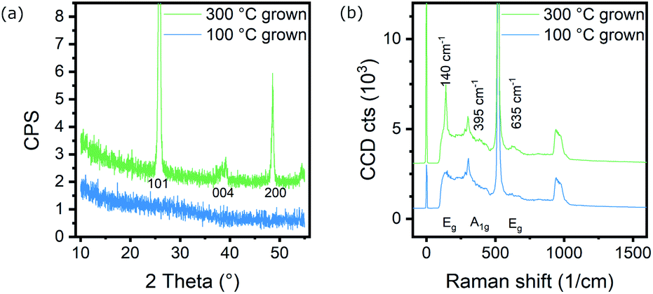 | ||
| Fig. 1 (a) X-ray diffractogram and (b) Raman spectrum of TiO2 films grown at 100 °C and 300 °C to yield amorphous or crystalline layers respectively. For the amorphous films, even the strongest signals indicating anatase at 25.3° and 140 cm−1 cannot be distinguished from the noise or fluorescent background. | ||
Corrosion at open-circuit in the dark and under different illumination conditions
Fig. 2 shows the residual film thicknesses after exposing the samples to a strongly acidic electrolyte (0.5 M H2SO4) for 2–60 h and the respective average etch rates, both in the dark and under illumination with 100 mW cm−2. It shows the steady decrease in film thickness over time, which is enhanced when the samples are illuminated. The average etch rates are 0.39–0.55 nm h−1 in the dark and up to 2.1 nm h−1 under illumination (Fig. 2b). | ||
| Fig. 2 (a) Residual thickness and (b) etch rate of TiO2 in 0.5 M H2SO4 over time in the dark (red) and under 100 mW cm−2 illumination (blue). | ||
To study the impact of incident wavelength, optical filters were used for experiments of 15 h etching under illumination. Using a longpass UV-filter with a 400 nm cut-on (Thorlabs FGL400) and considering that the band gap of TiO2 is >3 eV, exclusion of UV light should minimize photochemical or photoelectrochemical etching (any carriers generated by absorption in the degenerately doped silicon substrate are rapidly lost to recombination). The resulting etch rate was 1.4 nm h−1, close to the rate at full illumination. Using other filters, i.e. an UV-vis bandpass filter (Thorlabs FGS900, 900 nm cut-off) and an UV-passing filter (Thorlabs FGUV, transmission 325–385 nm & 700–900 nm) showed etch rates of 1.0 and 0.7 nm h−1, respectively, with no apparent influence of the chosen wavelength. Fig. 3a summarizes the average rates with several of the employed filters for experiments of 15 h etching duration at open-circuit (black frames).
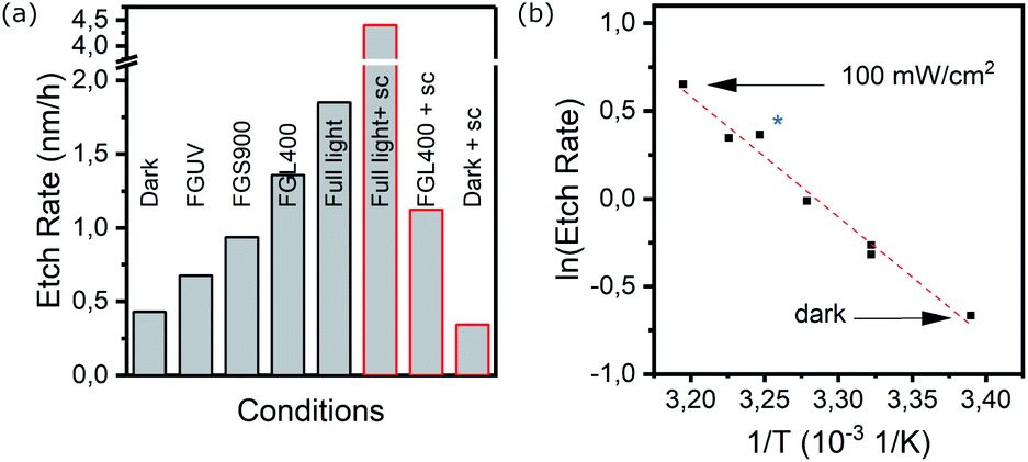 | ||
| Fig. 3 (a) Average etch rate over 15 h under full or partial illumination in 0.5 M H2SO4. FGL400, FGS900 and FGUV denote various filters to remove UV- and IR contributions from incoming light (L400/S900) or limit excitation to UV only (FGUV). “sc” indicates that the cell was wired directly to the Pt counter electrode to allow free transfer of photogenerated charge carriers. Due to higher etch rate, data for fully illuminated, short-circuited sample was determined after 4 hours of etching. (b) Arrhenius plot of TiO2 etch rate based on warming up of the PEC cell under illumination using various filters. The blue star indicates heating up of the cell, sample and electrolyte externally but in the dark (see text for details). All temperatures in the graph were measured within the electrolyte, close to the sample. With a slope of −6.873 × 10³ K−1, resulting in Ea = 57 kJ mol−1. | ||
A warming up of the PEC cell under constant illumination was noted and the electrolyte temperature in the cell was measured with a Pt-100 resistance thermometer, both in close proximity to the sample, with the sensor tip illuminated, and more remotely with the sensor not exposed to light. Without any filters, the measured temperatures rose to 38 °C and 41 °C with the sensor shadowed and exposed respectively (Fig. S8†). The surface temperature of the sample may even exceed those values but could not be determined directly.
The observed increased etch rates under illumination with and without various filters, indicated a temperature dependent etching rate, which was confirmed by performing experiments in the dark with a heated cell (approx. 38 °C electrolyte). In this case, the observed rate of 1.5 nm h−1 was comparable to the previously described experiment with the UV filter, for which a similar temperature was measured.
To verify the influence of temperature increase and stabilitzation during the early stage of continuous illumination, the TiO2 thickness was determined in a series of repeated 1 h intervals under illumination, showing an etch rate of 1.10 nm h−1 (Fig. S9†). A second series of measurements was performed at intervals of 2.8 h, each time allowing the cell to approach its saturation temperature, resulting in an etch rate of 1.63 nm h−1. As the reproducibility of the etch rates over 24 hours and 27 nm for the onset illumination conditions further shows, the slow initial corrosion rates are not linked to differences in the TiO2 film surface related to deposition conditions.
From the respective electrolyte temperatures determined under (partial) illumination and the resulting etch rates, an Arrhenius plot was constructed (Fig. 3b) which yields an activation energy of 57 kJ mol−1 for the dissolution of amorphous TiO2, comparable to the values reported for anatase-rutile particles in HF–HCl mixtures.27
Corrosion under short-circuit conditions
With the working electrode at open-circuit, electrochemical corrosion is expected to occur only if significant inhomogeneities are present. Such inhomogeneities, e.g. in the form of pinholes to the substrate or considerable phase differences, could present a difference in electrochemical potentials and divide the surface locally into microscopic anodic and cathodic regions that facilitate oxidation and reduction reactions. In our experiments, however, degradation proceeds isotropically, as evidenced by atomic force microscopy and spectroscopic ellipsometry mapping (Fig. S2 and S7†). On such a homogenous surfaces, the electrochemical anodic or cathodic corrosion would lead to a build-up of charges that result in an electrochemical potential that opposes further corrosion. Connecting the sample in short-circuit to a counter electrode or using a potentiostat in zero resistance mode, allows these charges to be extracted and the study of the influence of (photo-)electrochemical corrosion without applied bias.Results from the additional short-circuit experiments are included in Fig. 3a and highlighted by red frames. Under dark conditions but with the TiO2 electrode connected externally to the Pt counter electrode, the etch rate over 15 hours was largely unaffected and remained <0.5 nm h−1, while under full illumination, a corrosion of >4.0 nm h−1 was determined. Consequently, under short-circuit conditions and illumination, the etch process is accelerated more than 2-fold with the free flow of excess charge carriers to the counter electrode.
The importance of wavelength can herein be highlighted, as the use of the 400 nm cut-on filter during short-circuit experiments resulted in an etch rate of 1.2 nm h−1, comparable to the open-circuit conditions, and no apparent enhancement from extracting excess charge.
Considering the mechanism of photoinduced corrosion, with light dependent generation of reactive holes in the valence band that provide potential either for water oxidation or oxidation of the semiconductor, it is apparent that the increase in film removal under full illumination is related to excitation by photons of UV wavelength and energy greater than the band gap of the amorphous TiO2. The anodic decomposition potential of TiO2 is less positive than the potential at its valence band maximum (VBM), and more positive but close the redox potential of the oxygen evolution reaction (OER).28,29 With an intrinsically low activity towards water oxidation and immense overpotentials for oxygen evolution, the kinetic stability against photocorrosion, as was pointed out by Gerischer,30 and Bard,31 is overcome for these amorphous films.
Corrosion at different pH values
Studies for PEC absorber materials, catalysts and protection schemes are most commonly conducted in either very alkaline or very acidic electrolyte, due to the high conductivity of these solutions and often superior activity of the catalysts at the edges of the pH range.32In our experiments we have similarly observed significantly less degradation of the films at pH = 7 and even pH = 4, with a change in film thickness of <1 nm over 15 h of corrosion at open-circuit or 4 h allowing charge extraction. Instability in amorphous TiO2 films has also been reported for alkaline environments.33 In 1 M KOH or NaOH, the degradation of our samples proceeds inhomogeneously and is not easily determined through ellipsometry. It is uncertain at this point, if this is based on non-uniform degradation of the TiO2 layer or related to a pinhole induced photocorrosion process of the underlying substrate, as proposed by Didden et al. for thin films of TiO2 on CdS.11
In the range of pH = 0.3 to pH = 4, we determined the corrosion rates at OCP in the dark and under illumination and in zero resistance ammeter mode under illumination. Fig. 4 shows the resulting rates and highlights the pH influence for all measurement conditions. In the dark, corrosion rates drop from 0.51 nm h−1 at pH = 0.3 to 0.05 nm h−1 at pH = 2–3 and from 1.92 to 0.13 nm h−1 under illumination. With charge extraction, the corrosion rates remain higher by a factor of 2.5 to 4 compared to open-circuit but decrease rapidly with increasing pH value.
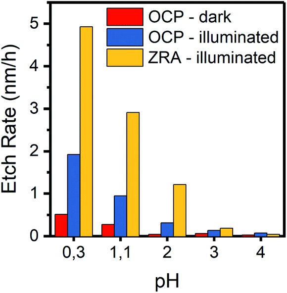 | ||
| Fig. 4 Etch rate dependence on the pH value of electrolyte (H2SO4 + K2SO4, 0.5 M SO42− total) at open-circuit conditions (OCP) and in zero resistance ammeter mode (ZRA). Data for OCP experiments all after 15 h, ZRA data for 4 or 8 h experiments due to higher etch rates. | ||
These findings agree well with Pourbaix diagrams that account for hydrated species of TiO2 and allow for TiO2+ or TiO2+ species at low pH.34,35 The common transitions here are the reduction to Ti3+ at potentials more favourable than proton reduction and oxidation towards a TiO22+ species approximately 700 mV more positive than the thermodynamic potential of oxygen evolution. Similarly, Knauss et al. have shown the hydrolysis of TiO2 even in rutile phase at elevated temperature to proceed through Ti(OH)4 to Ti(OH)3+ and Ti(OH)22+ in acidic media or to Ti(OH)5− in alkaline environment.36
Short comparison to other TiO2 thin films
The ALD growth of crystalline TiO2 proceeds through an initial amorphous thin film until achieving a critical thickness upon which fully crystalline films are generally observed.37,38 In the early growth phase, e.g. up to tens of nm – dependent on growth parameters – the amorphous layer hosts the seeds of crystallites, which progressively grow as anatase throughout the film both by continuous epitaxial growth at the exposed surface and crystallization through the film, consuming the amorphous TiO2.26The electrodes of the multi-crystalline films referenced for comparison in Fig. 1, that were grown at 300 °C and consist predominantly of anatase phase, exhibit no apparent corrosion even during extensive electrochemical testing. Other films, grown also at 300 °C but below the thickness threshold for full crystallisation show the degradation of the amorphous material only, while the embedded crystallites become successively more exposed39 which is in agreement with findings by other groups regarding the greater intrinsic stability of crystalline grown films.8
The solubility of Ti generally increases at pH values further from the point of zero charge (PZC) but the results show that this parameter is not an adequate indicator for comparing different phases.40 The PZC of amorphous TiO2 is commonly found to be more acidic (4.0–4.6)41,42 than either that for anatase (5.2–6.2)41,43 or rutile (5.4–6.0)43,44 and to change during aging and crystallisation.41
Structurally, amorphous TiO2 is more similar to anatase than rutile but the disorder in the chains of octahedra and the broad dispersion of bond lengths give rise to weak links in form of elongated Ti–O bonds with 1/2 to 1/3 of the bond-strength of the crystalline counterpart.45 Stability is additionally decreased by the lower average coordination numbers (CN) of oxygen and titanium (avg. CNTi = 5.49) in the amorphous phase compared to the crystalline phases (CNTi = 6).45
Sputtering profiles of XPS measurements (Fig. S10†) reveal low percentage impurity levels of carbon and nitrogen throughout the films originating from incompletely removed precursor ligands during the plasma-assisted deposition process. All films were exposed to atmosphere and show high contamination at the surface. The low temperature deposition at 100 °C results in higher levels of Nitrogen and Carbon contamination around 4 and 5 at%, in comparison to elevated deposition temperatures of 300 °C with impurity levels <1 at%.
The similar corrosion behaviour in 100 °C and 300 °C grown amorphous material points to a more dominant influence from the phase of TiO2, compared to the incorporation of N or C. Photoelectrochemically, our electrodes containing amorphous TiO2 commonly exhibit a reduction feature at 0.15 V vs. SHE (Fig. 5). This is only present after anodic polarization beyond a specific potential under illumination and has similar characteristics to a peak observed by Bertoluzzi et al. for Fe2O3.46 Their study attributes these peaks to the forced surface oxidation and the formation of traps, with further arguments towards a slow detrapping mechanism. For the TiO2 electrodes in this work, the appearance of reduction peaks coincides with the amorphous phase and instability of the material.
 | ||
| Fig. 5 Cyclic voltammogram (CV) of amorphous TiO2 on n++Si in the dark and under 100 mW cm−2 illumination. | ||
Preliminary insights from EIS
The study of electrochemical impedance spectroscopy (EIS) can shed further light on bias dependent capacitances and resistances in the electrochemical system. Models treating the charge transfer either directly from the bands or via surface states47,48 may help to identify bottlenecks, but were a poor approach to fitting the experimental data for our (partially) corroding electrodes. Instead, we focussed on simple equivalent circuits (Fig. 6a) for a blocking layer (dark) or single Randles circuit both containing one constant phase element (CPE) to account for inhomogeneity or mixed processes that cannot at this stage be fully unravelled.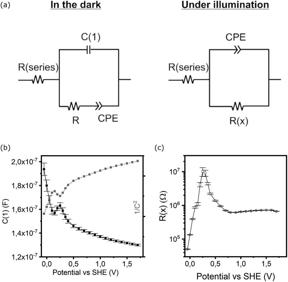 | ||
| Fig. 6 (a) Electrochemical equivalent circuits used for modelling EIS data, (b) capacitive element in parallel (C1) in the dark and (c) main resistance element under illumination. | ||
The potential dependent analysis of the separate elements (Fig. 6b and c) reveals several features that can be linked to the CV scans (Fig. 5):
(1) The pure capacitance C(1) encountered in the model in the dark exhibits a dip at the exact potential of the reductive peak in the CV (0.15 V), or a local maximum at 0.25 V (Fig. 6b).
(2) The CPE based capacitance and resistance sharply change in parallel with the onset of reductive current (<0.2 V).
(3) Under illumination, the dominant capacitance (derived from the CPE), though generally an order of magnitude larger, has a minor peak at 0.15 V and a maximum of resistance at 0.25 V vs. SHE (Fig. 6c).
In line with any modelling of complex data, the analysis of electrochemical impedance spectroscopy offers numerous pitfalls and is susceptible to assumptions in selecting an appropriate electrochemical equivalent circuit. In order to justify a more comprehensive model, systematic variations of the layer studied and the overall electrochemical system are required to attribute physical significance to any selected element. In a comprehensive study currently ongoing, we expect to shed light on the contributing factors to the chemical and photoelectrochemical corrosion, as well as a link to the intricate interplay of deposition parameters in film growth by ALD. This could help identify the optimal deposition pathway to stable protective coatings for photoanodes and cathodes, as well as provide means to identify weak points in electrochemically exposed layers.
Conclusions
The corrosion of ALD-grown, amorphous TiO2 films in 0.5 M sulfuric acid (pH = 0.3) was studied by spectroscopic ellipsometry. At open-circuit potential the etch rate in the dark is 0.5 nm h−1. Under 100 mW cm−2 illumination, the etch rate increases to 2.1 nm h−1, which can be attributed to the temperature change of the photoelectrochemical cell under continuous illumination from room temperature to 41 °C. By using cut-on and cut-off filters to remove different fractions of the spectrum (e.g. UV or IR), it could be shown that excitation wavelength is not responsible for an increase in etch rates but rather the different cell temperatures resulting from illumination. The corresponding activation energy of the TiO2 dissolution is 57 kJ mol−1.Controlling the flow of excess generated charge carriers in short-circuit configuration, as opposed to open-circuit conditions, furthermore revealed a photoelectrochemical corrosion contribution dependent on UV excitation, increasing etch rates more than twofold. In agreement with recently published Pourbaix diagrams that account for hydrated TiO2, the degradation is strongly pH dependent and becomes negligible at pH = 4 in the time frames investigated. Consequently, in order to ensure long term stability, for PEC devices operating in acidic electrolyte, and incorporating amorphous TiO2 coatings which are at least partially in contact with the electrolyte, the operational conditions should be limited to pH > 4.
In comparison to the stable, crystalline counterpart anatase, amorphous TiO2 shows a photoinduced reduction peak near 0.2 V vs. SHE that can be linked to features in the EIS analysis. Ongoing comprehensive studies in this direction may be helpful to identify the exact origin of the instability in TiO2 films, their dependence on synthesis parameters and electrochemical contribution in the overall system.
Altogether, the results show that for PEC systems a study of the electrodes without added catalyst or enabled photoreaction can reveal underlying stability limitations.
Author contributions
The manuscript was written through contributions of all authors. All authors have given approval to the final version of the manuscript and declare no competing interests.Conflicts of interest
There are no conflicts to declare.Acknowledgements
The authors are grateful to A. Schwartzberg, D. Olynick, and S. Cabrini for their insight and support for the preparation and coating of the samples by atomic layer deposition at The Molecular Foundry of the Lawrence Berkeley National Laboratory. The authors furthermore gratefully acknowledge the financial support by the Federal Ministry of Education and Research of Germany in the framework of the project “FocusH2” (no. 03SF0479A). Work at the Molecular Foundry was supported by the Office of Science, Office of Basic Energy Sciences, of the U.S. Department of Energy under contract no. DE-AC02-05CH11231.Notes and references
- S. Hu, N. S. Lewis, J. W. Ager, J. Yang, J. R. McKone and N. C. Strandwitz, J. Phys. Chem. C, 2015, 119, 24201–24228 CrossRef CAS.
- Y. W. Chen, J. D. Prange, S. Dühnen, Y. Park, M. Gunji, C. E. D. Chidsey and P. C. McIntyre, Nat. Mater., 2011, 10, 539–544 CrossRef CAS PubMed.
- B. Seger, T. Pedersen, A. B. Laursen, P. C. K. Vesborg, O. Hansen and I. Chorkendorff, J. Am. Chem. Soc., 2013, 135, 1057–1064 CrossRef CAS PubMed.
- S. Hu, M. R. Shaner, J. A. Beardslee, M. Lichterman, B. S. Brunschwig and N. S. Lewis, Science, 2014, 344, 1005–1009 CrossRef CAS PubMed.
- J. Qiu, G. Zeng, M.-A. Ha, B. Hou, M. Mecklenburg, H. Shi, A. N. Alexandrova and S. B. Cronin, Chem. Mater., 2015, 27, 7977–7981 CrossRef CAS.
- M. F. Lichterman, A. I. Carim, M. T. McDowell, S. Hu, H. B. Gray, B. S. Brunschwig and N. S. Lewis, Energy Environ. Sci., 2014, 7, 3334–3337 RSC.
- L. Rovelli, S. D. Tilley and K. Sivula, ACS Appl. Mater. Interfaces, 2013, 5, 8018–8024 CrossRef CAS PubMed.
- A. Paracchino, N. Mathews, T. Hisatomi, M. Stefik, S. David Tilley and M. Grätzel, Energy Environ. Sci., 2012, 5, 8673–8681 RSC.
- B. Seger, S. David Tilley, T. Pedersen, P. C. K. Vesborg, O. Hansen, M. Grätzel and I. Chorkendorff, J. Mater. Chem. A, 2013, 1, 15089–15094 RSC.
- B. Seger, D. S. Tilley, T. Pedersen, P. C. K. Vesborg, O. Hansen, M. Grätzel and I. Chorkendorff, RSC Adv., 2013, 3, 25902–25907 RSC.
- A. Didden, P. Hillebrand, B. Dam and R. van de Krol, Int. J. Photoenergy, 2015, 2015, 1–8 CrossRef.
- C. Ros, T. Andreu, M. D. Hernández-Alonso, G. Penelas-Pérez, J. Arbiol and J. R. Morante, ACS Appl. Mater. Interfaces, 2017, 9, 17932–17941 CrossRef CAS PubMed.
- M. Hannula, H. Ali-Löytty, K. Lahtonen, E. Sarlin, J. Saari and M. Valden, Chem. Mater., 2018, 30, 1199–1208 CrossRef CAS PubMed.
- J. Ohkubo, Y. Hirose, E. Sakai, S. Nakao, T. Hitosugi and T. Hasegawa, Jpn. J. Appl. Phys., 2011, 50, 018002 CrossRef.
- S. Okazaki, T. Ohhashi, S. Nakao, Y. Hirose, T. Hitosugi and T. Hasegawa, Jpn. J. Appl. Phys., 2013, 52, 098002 CrossRef.
- S. M. Kramer, I. G. Gorichev, Yu. A. Lainer, I. V. Artamonova and M. V. Terekhova, Russian Metallurgy, 2014, 2014, 704–707 CrossRef.
- E. V. Shkol’nikov, Russ. J. Phys. Chem. A, 2016, 90, 567–571 CrossRef.
- F. Nandjou and S. Haussener, J. Phys. D: Appl. Phys., 2017, 50, 124002 CrossRef.
- F. Nandjou and S. Haussener, ChemSusChem, 2019, 12, 1984–1994 CrossRef CAS PubMed.
- E. Langereis, S. B. S. Heil, H. C. M. Knoops, W. Keuning, M. C. M. van de Sanden and W. M. M. Kessels, J. Phys. D: Appl. Phys., 2009, 42, 073001 CrossRef.
- A. S. Ferlauto, G. M. Ferreira, J. M. Pearce, C. R. Wronski, R. W. Collins, X. Deng and G. Ganguly, J. Appl. Phys., 2002, 92, 2424–2436 CrossRef CAS.
- J. Price, P. Y. Hung, T. Rhoad, B. Foran and A. C. Diebold, Appl. Phys. Lett., 2004, 85, 1701–1703 CrossRef CAS.
- G. E. Jellison and F. A. Modine, Appl. Phys. Lett., 1996, 69, 371–373 CrossRef CAS.
- C. M. Herzinger, B. Johs, W. A. McGahan, J. A. Woollam and W. Paulson, J. Appl. Phys., 1998, 83, 3323–3336 CrossRef CAS.
- W.-J. Lee and M.-H. Hon, J. Phys. Chem. C, 2010, 114, 6917–6921 CrossRef CAS.
- G. Luka, B. S. Witkowski, L. Wachnicki, M. Andrzejczuk, M. Lewandowska and M. Godlewski, CrystEngComm, 2013, 15, 9949–9954 RSC.
- E. Bright and D. W. Readey, J. Am. Ceram. Soc., 1987, 70, 900–906 CrossRef CAS.
- H. Gerischer, J. Vac. Sci. Technol., 1978, 15, 1422–1428 CrossRef CAS.
- S. Chen and L.-W. Wang, Chem. Mater., 2012, 24, 3659–3666 CrossRef CAS.
- H. Gerischer, J. Electroanal. Chem. Interfacial Electrochem., 1977, 82, 133–143 CrossRef CAS.
- A. J. Bard and M. S. Wrighton, J. Electrochem. Soc., 1977, 124, 1706 CrossRef CAS.
- Z. Chen, H. Dinh and E. Miller, Photoelectrochemical Water Splitting: Standards, Experimental Methods, and Protocols, Springer-Verlag, New York, 2013 Search PubMed.
- J. Zheng, Y. Lyu, R. Wang, C. Xie, H. Zhou, S. P. Jiang and S. Wang, Nat. Commun., 2018, 9, 1–10 CrossRef CAS PubMed.
- M. Pourbaix, Atlas of electrochemical equilibria in aqueous solutions, Nat'L Assoc. Of Corrosion, 1974 Search PubMed.
- P. Acevedo-Peña, J. Vazquez-Arenas, R. Cabrera-Sierra, L. Lartundo-Rojas and I. González, J. Electrochem. Soc., 2013, 160, C277–C284 CrossRef.
- K. G. Knauss, M. J. Dibley, W. L. Bourcier and H. F. Shaw, Appl. Geochem., 2001, 16, 1115–1128 CrossRef CAS.
- D. R. G. Mitchell, D. J. Attard and G. Triani, Thin Solid Films, 2003, 441, 85–95 CrossRef CAS.
- A. P. Alekhin, S. A. Gudkova, A. M. Markeev, A. S. Mitiaev, A. A. Sigarev and V. F. Toknova, Appl. Surf. Sci., 2010, 257, 186–191 CrossRef CAS.
- R. Raudsepp, H. Kriegel, J. Kollmann, T. Klassen and M. Schieda, manuscript in preparation.
- M. P. Finnegan, H. Zhang and J. F. Banfield, Chem. Mater., 2008, 20, 3443–3449 CrossRef CAS.
- E. A. Barringer and H. K. Bowen, Langmuir, 1985, 1, 414–420 CrossRef CAS.
- T. Sugimoto and X. Zhou, J. Colloid Interface Sci., 2002, 252, 347–353 CrossRef CAS PubMed.
- K. Bourikas, T. Hiemstra and W. H. Van Riemsdijk, Langmuir, 2001, 17, 749–756 CrossRef CAS.
- M. L. Machesky, D. J. Wesolowski, D. A. Palmer and K. Ichiro-Hayashi, J. Colloid Interface Sci., 1998, 200, 298–309 CrossRef CAS.
- J. Mavračić, F. C. Mocanu, V. L. Deringer, G. Csányi and S. R. Elliott, J. Phys. Chem. Lett., 2018, 9, 2985–2990 CrossRef PubMed.
- L. Bertoluzzi, L. Badia-Bou, F. Fabregat-Santiago, S. Gimenez and J. Bisquert, J. Phys. Chem. Lett., 2013, 4, 1334–1339 CrossRef CAS PubMed.
- B. Klahr, S. Gimenez, F. Fabregat-Santiago, T. Hamann and J. Bisquert, J. Am. Chem. Soc., 2012, 134, 4294–4302 CrossRef CAS PubMed.
- L. Bertoluzzi, P. Lopez-Varo, J. A. J. Tejada and J. Bisquert, J. Mater. Chem. A, 2016, 4, 2873–2879 RSC.
Footnote |
| † Electronic supplementary information (ESI) available. See DOI: 10.1039/d0ta04878j |
| This journal is © The Royal Society of Chemistry 2020 |