
Extraordinarily long diffusion length in PM6:Y6 organic solar cells
Nurlan
Tokmoldin
 a,
Seyed Mehrdad
Hosseini
a,
Meysam
Raoufi
b,
Le Quang
Phuong
a,
Oskar J.
Sandberg
c,
Huilan
Guan
d,
Yingping
Zou
d,
Dieter
Neher
b and
Safa
Shoaee
*a
a,
Seyed Mehrdad
Hosseini
a,
Meysam
Raoufi
b,
Le Quang
Phuong
a,
Oskar J.
Sandberg
c,
Huilan
Guan
d,
Yingping
Zou
d,
Dieter
Neher
b and
Safa
Shoaee
*a
aOptoelectronics of Disordered Semiconductors, Institute of Physics and Astronomy, University of Potsdam, Karl-Liebknecht-Straße 24-25, Potsdam-Golm 14476, Germany. E-mail: shoai@uni-potsdam.de; tokmoldin@uni-potsdam.de
bSoft Matter Physics, Institute of Physics and Astronomy, University of Potsdam, Karl-Liebknecht-Straße 24-25, Potsdam-Golm 14476, Germany
cDepartment of Physics, Swansea University, Singleton Park, Swansea, SA2 8PP, Wales, UK
dCollege of Chemistry and Chemical Engineering, Central South University, Changsha 410083, P. R. China
First published on 1st April 2020
Abstract
The PM6:Y6 bulk-heterojunction (BHJ) blend system achieves high short-circuit current (JSC) values in thick photovoltaic junctions. Here we analyse these solar cells to understand the observed independence of the short-circuit current upon photoactive layer thickness. We employ a range of optoelectronic measurements and analyses, including Mott–Schottky analysis, CELIV, photoinduced absorption spectroscopy, mobility measurements and simulations, to conclude that, the invariant photocurrent for the devices with different active layer thicknesses is associated with the Y6's diffusion length exceeding 300 nm in case of a 300 nm thick cell. This is despite unintentional doping that occurs in PM6 and the associated space-charge effect, which is expected to be even more profound upon photogeneration. This extraordinarily long diffusion length – which is an order of magnitude larger than typical values for organics – dominates transport in the flat-band region of thick junctions. Our work suggests that the performance of the doped PM6:Y6 organic solar cells resembles that of inorganic devices with diffusion transport playing a pivotal role. Ultimately, this is expected to be a key requirement for the fabrication of efficient, high-photocurrent, thick organic solar cells.
Introduction
In 2019, the non-fullerene acceptor (NFA) Y6 blended with PM6 achieved power conversion efficiencies (PCE) of 15%.1 In 2020 Y6 blended with an alternative polymer gave 17.6% certified efficiency.2 With the PCE of NFA based organic photovoltaic devices reaching the performance level of first-generation polycrystalline silicon technologies, the feasibility of commercial solutions is becoming increasingly realistic.3–5 One of the significant obstacles which must still be overcome en route to commercialization is the low thickness of most typical organic active layers which rarely exceeds the 100 nm range.6 Determination of, and addressing the causes of such limitations requires building a general energetic picture of photovoltaic semiconductor junctions, which is a very important tool for understanding of the role of different materials and electronic processes. Conventional understanding of solar cell operation which has been initiated and driven by the studies of inorganic crystalline materials is mainly based on the models of the p–n junction and p–i–n solar cell, where the electric field is of little relevance for charge collection at short circuit, while instead charge separation relies on interfacial kinetics, energy steps at interfaces and diffusion driven transport.7,8 However with the discovery of the bulk heterojunction organic solar cells (BHJ), due to the low charge mobilities and low diffusion coefficients (the charge carrier diffusion lengths are typically <20 nm (ref. 9–11)) a series of new device models has been established where the role of charge collection by electric fields (drift transport) is essential to the solar cell performance, since purely diffusive transport does not lead to efficient charge extraction.12 One consequence of this reliance on drift transport is that organic solar cells are typically thin – on the order of hundreds of nanometres – compared to their inorganic counterparts – microns to tens of microns thick cells. In this regard, it has previously been shown that low charge mobilities may consequently limit both the short-circuit current (JSC) and the fill factor (FF) of organic solar cells.9,13,14 In particular, organic bulk heterojunctions typically show lower JSC values for thicknesses above a particular threshold, despite an increase in the number of absorbed photons.11Among the organic blends demonstrating promising output characteristics at higher active layer thicknesses, the PM6:Y6 (PM6: poly[(2,6-(4,8-bis(5-(2-ethylhexyl-3-fluoro)thiophen-2-yl)-benzo[1,2-b:4,5-b′]dithiophene))-alt-(5,5-(1′,3′-di-2-thienyl-5′,7′-bis(2-ethylhexyl)benzo [1′,2′-c:4′,5′-c′]dithiophene-4,8-dione))]; Y6: 2,2′-((2Z,2′Z)-((12,13-bis(2-ethylhexyl)-3,9-diundecyl-12,13-dihydro-[1,2,5]thiadiazolo[3,4-e]thieno[2′′,3′′:4′,5′]-thieno[2′,3′:4,5]pyrrolo [3,2-g]thieno[2′,3′:4,5]thieno[3,2-b]indole-2,10-diyl)bis(methanylylidene))-bis(5,6-difluoro-3-oxo-2,3-dihydro-1H-indene-2,1-diylidene))dimalononitrile) NFA based blend has recently gained much attention showing PCE of around 15% in 100 nm and even still impressive 13% for the 300 nm thick active layer devices.1 We have previously studied the mechanism of charge generation in a 100 nm thick PM6:Y6 device and found that photocurrent generation is essentially barrierless with near-unity efficiency. Theoretical modelling suggests that efficient charge separation is related to the ability of Y6 to form crystalline domains in the optimized blend. Thereby, the dissociation of the interfacial CT state is assisted by an electrostatic interfacial field which for crystallized Y6 is large enough to compensate the Coulomb dissociation barrier.15 Profiting from this crystallinity effect are the high JSC and electron mobility values obtained in the PM6:Y6 blends. However, a question of interest which still remains lucid is how the photocurrent depends on thickness, particularly in thicker junctions. The observed constant JSC for different active layer thicknesses indicates insignificant bimolecular recombination.9,16 In this paper, we employ Mott–Schottky analysis of the PM6:Y6 depletion region, supported by CELIV, to study the thickness dependence of the device behaviour. To interpret the experimental observations, we use numerical simulations that incorporate the effect of doping on the device electrostatics. We demonstrate that high performance in thicker PM6:Y6 devices is due to the significantly enhanced electron diffusion length, enabling efficient operation even for doped blends.
Experimental
Device fabrication
PM6 was purchased from 1-material and Y6 was provided by Central South University and synthesized according to literature.1 For device fabrication, ITO-coated glass substrates were cleaned in an ultrasonic bath using detergent, deionized water, acetone and isopropyl alcohol (IPA), the dried substrates were treated by oxygen plasma at room temperature for 4 min. PEDOT:PSS (poly(3,4-ethylenedioxythiophene):poly(styrene sulfonate)) (Baytron PVP Al 4083) was spin-coated on ITO and annealed for 15 min at 150 °C in the air. PM6 and Y6 were mixed in the 1![[thin space (1/6-em)]](https://www.rsc.org/images/entities/char_2009.gif) :1.2 proportion, dissolved in chloroform and, following addition of 1-chloronaphthalene (CN) (0.5% by volume), spin-cast on top of PEDOT:PSS. An electron-injecting interlayer of PDINO was then spin-cast onto the active layer from the 1 mg mL−1 solution in methanol. The Ag top electrode was thermally deposited in vacuum at the base pressure of ca. 10−6 mbar. The device fabrication was completed by glass-on-glass encapsulation in order to perform measurements in the air.
:1.2 proportion, dissolved in chloroform and, following addition of 1-chloronaphthalene (CN) (0.5% by volume), spin-cast on top of PEDOT:PSS. An electron-injecting interlayer of PDINO was then spin-cast onto the active layer from the 1 mg mL−1 solution in methanol. The Ag top electrode was thermally deposited in vacuum at the base pressure of ca. 10−6 mbar. The device fabrication was completed by glass-on-glass encapsulation in order to perform measurements in the air.
Characterization
Results and discussion
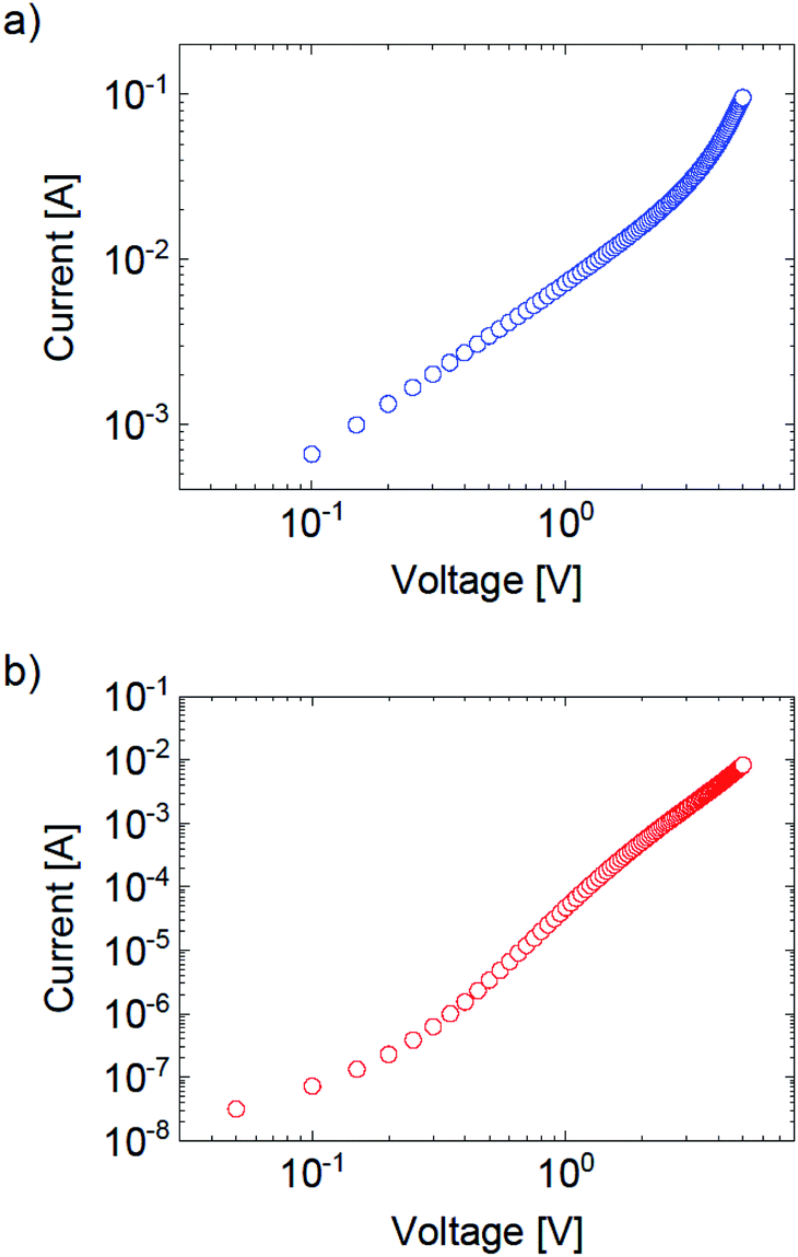
For comparison of operation of thin and thick PM6:Y6 devices two active layer thicknesses of 100 nm and 300 nm were employed. Fig. 1 shows the J–V curves of the two devices in the dark and under 1 sun illumination. Similar to the results reported previously,1 the increase in the active layer thickness in these standard architecture devices does not cause a notable change in the VOC and JSC, while the FF is reduced, albeit less significantly than what is typically observed in organic photovoltaic blends.11 Whilst the drop in the FF can be assigned to increased recombination, it is striking that the JSC barely changes with thickness up to several hundreds of nanometers. This observation is different to most other organic systems where the JSC increases due to enhanced light absorption until the optimum value at a finite junction thickness, followed by noticeable decrease (such as in the case of PCDTBT) for thicknesses thereafter.11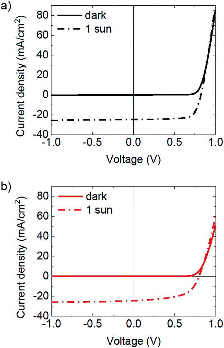 | ||
| Fig. 1 J–V characteristics of the PM6:Y6 devices with active layer thicknesses of 100 nm (a) and 300 nm (b). | ||
Fig. 2 shows the external quantum efficiencies of the two devices. It can be seen that consistent with the invariant JSC, the EQE also remains significantly unchanged in magnitude across the entire wavelength spectrum.
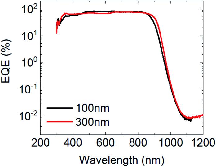 | ||
| Fig. 2 External quantum efficiency spectra of the PM6:Y6 devices with active layer thicknesses of 100 nm and 300 nm. | ||
It has previously been shown that photocurrent generation in organic solar cells can be correlated with the depletion layer width with respect to the junction thickness.11,18 Thus, undoped devices with the depletion region extending throughout the active layer are expected to show better performance than the doped devices with similar device architecture.19 To determine the depletion region in the device, capacitance–voltage experiments were performed. Capacitance–voltage measurements are an established technique used to determine the doping density of a semiconductor.20 The capacitance–voltage analysis of organic solar cells, based on Mott–Schottky formalism, enables to obtain some of the important device parameters, including active layer doping, depletion layer width etc., thereby helping to build a more comprehensive model of the device operation.18 By conducting the measurements in the dark, where the mobility of the carriers does not affect the device electrostatics, we can establish the depletion region caused by unintentional doping rather than a mobility imbalance.17,18
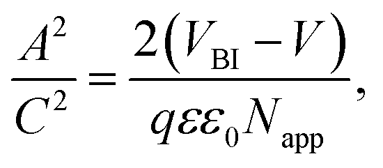
The results of the capacitance–voltage experiments in the dark and the Mott–Schottky plots for the 100 nm and 300 nm devices, along with the derivative doping profiles across the active layer width are demonstrated in Fig. 3. The doping profiles were obtained similarly to ref. 15 and 16. The linear descending region of the Mott–Schottky plot in Fig. 3a and b is expected to follow the expression:
 | (1) |
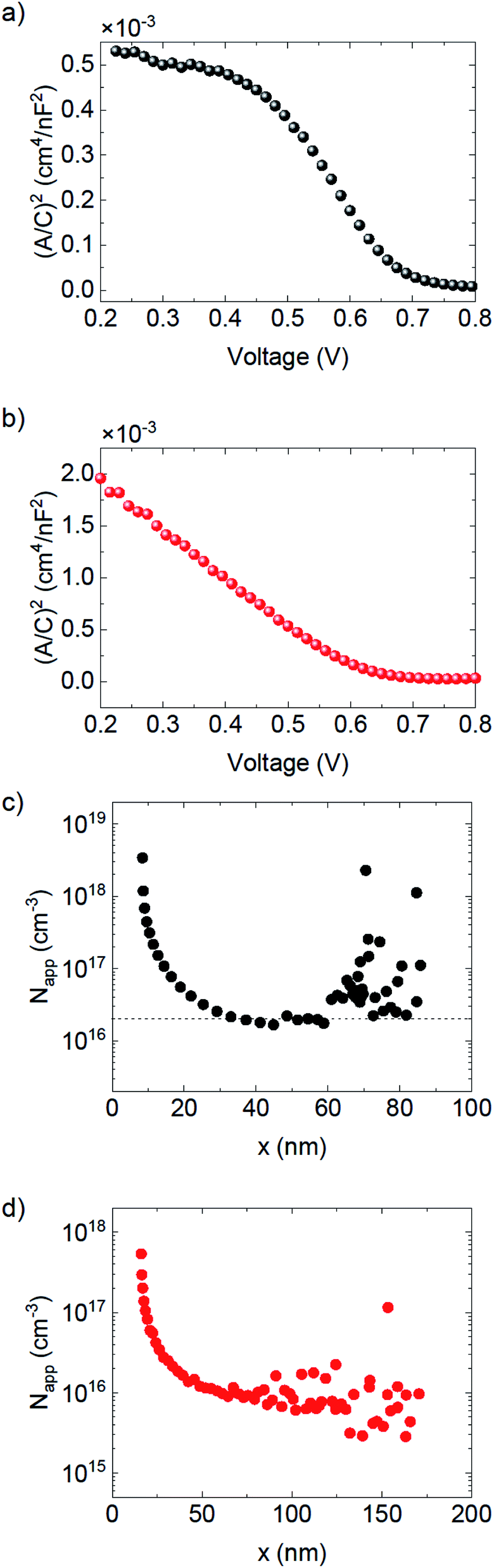 | ||
| Fig. 3 Mott–Schottky plots (a and b) and apparent doping profiles (c and d) of the PM6:Y6 devices with active layer thicknesses of 100 nm (a and c) and 300 nm (b and d). | ||
The doping concentration in the 300 nm PM6:Y6 device was confirmed via the charge extraction by linearly increasing voltage (CELIV)23 measurements, yielding the value of 8.7 × 1015 cm−3. An experimental current density transient in Fig. 4 is presented in the form of j−2 as a function of (Rt + Uoff), where R is the pulse ramp-up rate, t is time, and Uoff is the offset voltage. The pulse ramp-up rate of 0.8 V/50 μs and the offset voltage of −0.5 V were used in the measurement. The red line represents a linear fit, enabling to estimate the carrier concentration via expression:
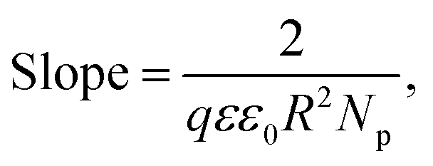 | (2) |
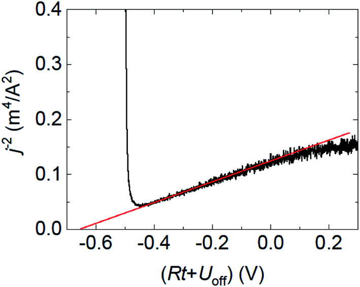 | ||
| Fig. 4 Experimental current density transient obtained in the CELIV measurement for the 300 nm thick PM6:Y6 device at the pulse ramp-up rate of 0.8 V/50 μs and the offset voltage of −0.5 V. | ||
The C–V measurements enable to estimate the width of the depletion region x via
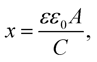 | (3) |
The above depletion width picture is confirmed by simulations of the device band diagrams and the J–V characteristics, using AFORS-HET,25 where the active layer doping level obtained from the Mott–Schottky analysis was employed (see Table 1 for simulation parameter details). The respective simulated energy band diagrams taking into account the impact of doping on band bending within the active layer are given in Fig. 5. The J–V curves for both thicknesses could be well reproduced with the same set of parameters, confirming the correctness of the model. Note that most values in Table 1 were taken from experiments, and only slightly adjusted to obtain the best agreement with the J–V curves. It is evident, that while the 100 nm cell is almost fully depleted at JSC (V = 0 V), resulting in the electric field which extends across the whole width of the active layer, in the 300 nm cell the active layer is only partly depleted. In the thick device, the depletion region will occupy about half of the active layer closest to the cathode. The remaining half of the device thickness is defined as the neutral region and in this part of the device there is little electric field. Therefore, while in the 100 nm cell the dominant charge transport mechanism is bound to be the drift of the carriers, for the 300 nm device however, carrier diffusion has to play a more significant role in order to avoid loss in the photocurrent.
| Parameter | PEDOT:PSS | PM6:Y6 | PDINO |
|---|---|---|---|
| Thickness [nm] | 30 | 100, 300 | 5 |
| Relative dielectric constant | 2.2 | 3.5 | 5 |
| Band gap [eV] | 3.0 | 1.27 | 2.6 |
| Electron affinity [eV] | 2.2 | 4.1 | 3.7 |
| Effective density of states [cm−3] | 1021 | 1020 | 1.5 × 10²⁰ |
| Band-to-band recombination coefficient [cm3 s−1] | 1.7 × 10⁻¹¹ | ||
| Electron mobility [cm2 V−1 s−1] | 10−7 | 1–2.5 × 10⁻³ | 5 × 10⁻¹ |
| Hole mobility [cm2 V−1 s−1] | 0.77 | 2 × 10⁻⁴ | 10−7 |
| Doping concentration [cm−3] | 2.25 × 10²⁰ | 8 × 10¹⁵ | 1010 |
| Anode hole surface recombination velocity [cm s−1] | 107 | — | — |
| Anode electron surface recombination velocity [cm s−1] | 102 | — | — |
| Cathode electron surface recombination velocity [cm s−1] | — | — | 107 |
| Cathode hole surface recombination velocity [cm s−1] | — | — | 102 |
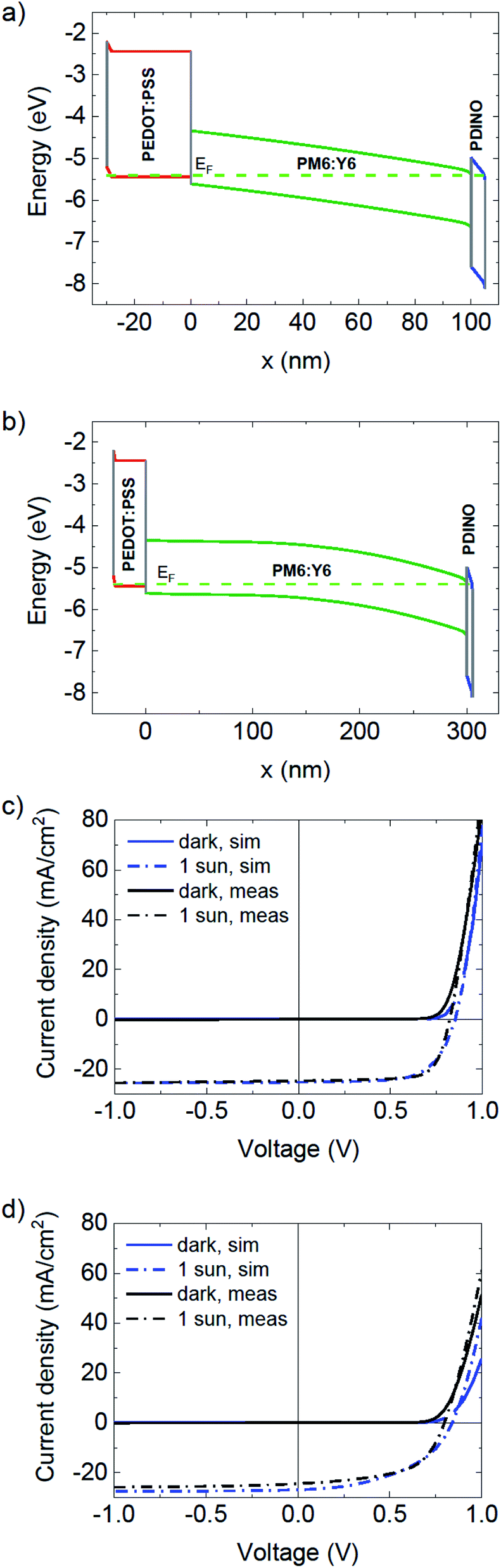 | ||
| Fig. 5 Simulated energy band diagrams at the “short circuit” condition (a and b) and comparison of simulated and measured J–V characteristics (c and d) of the PM6:Y6 devices with active layer thicknesses of 100 nm (a and c) and 300 nm (b and d). See Table 1 for simulation parameter details. | ||
Typically in inorganic thin film solar cells, the ratio x/d varies from around 10% in Cu(In,Ga)Se2 (CIGS) to 100% in fully depleted devices like amorphous Si.26–28 When going from small to large values of x/d, the mechanism by which charge generation occurs changes. While devices with low x/d are controlled by diffusion such as in the case of c-Si and dye-sensitized solar cells (DSSC), the larger the space charge region becomes relative to the absorber thickness, as in a typical 100 nm organic solar cell, the more drift will affect charge carrier collection.
The diffusion length, ld can be calculated using the formula:
 | (4) |
 | ||
| Fig. 6 Space-charge limited current (SCLC) vs. voltage curves for the 300 nm-thick PM6:Y6 devices with the following structures: (a) ITO/ZnO/PM6:Y6/PDINO/Ag, (b) ITO/PEDOT:PSS/PM6:Y6/MoO3/Au. | ||
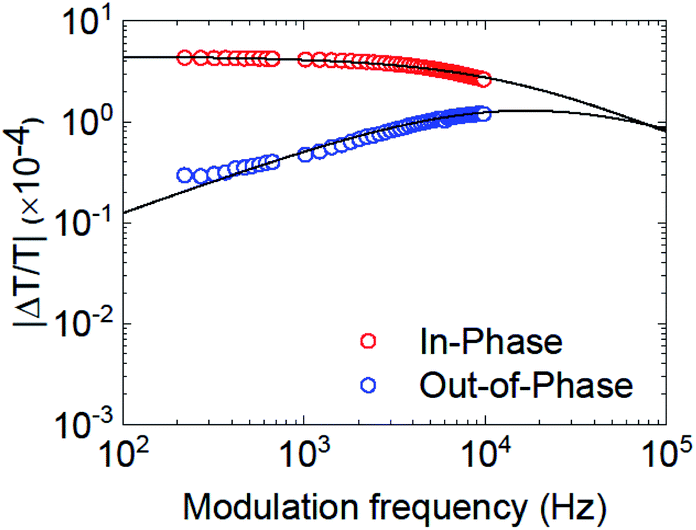 | ||
| Fig. 7 Photoinduced absorption spectroscopy characteristics of the ITO/PEDOT:PSS/PM6:Y6/PDINO/Ag (35 nm) photovoltaic devices at the open circuit condition. Global fitting of the measured in-phase and out-of-phase data points provides the average carrier lifetime value of 9.8 × 10⁻⁶ s. | ||
Our analyses above show that PM6:Y6 exhibits high electron mobility and slow carrier recombination which result in the large carrier diffusion length. This diffusion length is greater than the width of the flat-band region and can be responsible for the efficient photocurrent in thick junctions where the depletion region does not extend over the entire active layer thickness. In this respect, the operation of the thicker PM6:Y6 device resembles that of conventional silicon cells and DSSCs, in terms of a significant part of the active layer remaining in the flat-band condition and charge transport relying mainly on diffusion. Another advantage of the long diffusion length and low x/d, is the reduced Shockley–Read–Hall (SRH) recombination in the neutral region, since the minority carrier concentration is smaller than the majority carrier concentration.34
Conclusions
In conclusion, using the Mott–Schottky analysis of 100 and 300 nm PM6:Y6 solar cells, supplemented by mobility, PIA measurements and simulations, this paper puts the spotlight on carrier diffusion as an important charge transport mechanism facilitating efficient operation of devices with higher active layer thickness. Specifically, the impact of enhanced carrier diffusion is expected to be significant for doped active layers, with the present work estimating the doping concentration of the order of 1016 cm−3 for the used PM6:Y6 batch. Although such doping levels would still be compatible with the depletion region extending throughout the whole active layer width within the thinner devices, for the thicker devices it would result in the significant part of the active layer remaining at “flat band”, i.e. with almost no electric field driving carrier transport. In this case, enhanced diffusion, via high carrier mobilities, appears to play an important part in carrier transport, resulting in the better-than-expected device performance.Conflicts of interest
There are no conflicts to declare.Acknowledgements
We express our gratitude to the Alexander von Humboldt Foundation for funding. Y. Z. acknowledges the grant of the National Natural Science Foundation of China (21875286).Notes and references
- J. Yuan, Y. Zhang, L. Zhou, G. Zhang, H.-L. Yip, T.-K. Lau, X. Lu, C. Zhu, H. Peng, P. A. Johnson, M. Leclerc, Y. Cao, J. Ulanski, Y. Li and Y. Zou, Joule, 2019, 3, 1140–1151 CrossRef CAS.
- Q. Liu, Y. Jiang, K. Jin, J. Qin, J. Xu, W. Li, J. Xiong, J. Liu, Z. Xiao, K. Sun, S. Yang, X. Zhang and L. Ding, Sci. Bull., 2020, 65, 272–275 CrossRef.
- S. Narayanan, J. Zolper, F. Yun, S. R. Wenham, A. B. Sproul, C. M. Chong and M. A. Green, in IEEE Conference on Photovoltaic Specialists, 1990, vol. 1, pp. 678–680 Search PubMed.
- L. Zhan, S. Li, T.-K. Lau, Y. Cui, X. Lu, M. Shi, C.-Z. Li, H. Li, J. Hou and H. Chen, Energy Environ. Sci., 2020, 13, 635–645 RSC.
- J. Song, C. Li, L. Zhu, J. Guo, J. Xu, X. Zhang, K. Weng, K. Zhang, J. Min, X. Hao, Y. Zhang, F. Liu and Y. Sun, Adv. Mater., 2019, 31, 1905645 CrossRef CAS PubMed.
- P. R. Berger and M. Kim, J. Renewable Sustainable Energy, 2018, 10, 13508 CrossRef.
- P. Würfel, Physics of Solar Cells: From Principles to New Concepts, John Wiley and Sons, 2007 Search PubMed.
- J. Bisquert, D. Cahen, G. Hodes, S. Rühle and A. Zaban, J. Phys. Chem. B, 2004, 108, 8106–8118 CrossRef CAS.
- T. Kirchartz, T. Agostinelli, M. Campoy-Quiles, W. Gong and J. Nelson, J. Phys. Chem. Lett., 2012, 3, 3470–3475 CrossRef CAS PubMed.
- R. A. Street, M. Schoendorf, A. Roy and J. H. Lee, Phys. Rev. B: Condens. Matter Mater. Phys., 2010, 81, 205307 CrossRef.
- J. Wu, J. Luke, H. K. H. Lee, P. Shakya Tuladhar, H. Cha, S.-Y. Jang, W. C. Tsoi, M. Heeney, H. Kang, K. Lee, T. Kirchartz, J.-S. Kim and J. R. Durrant, Nat. Commun., 2019, 10, 5159 CrossRef PubMed.
- S. R. Cowan, N. Banerji, W. L. Leong and A. J. Heeger, Adv. Funct. Mater., 2012, 22, 1116–1128 CrossRef CAS.
- D. Bartesaghi, I. d. C. Pérez, J. Kniepert, S. Roland, M. Turbiez, D. Neher and L. J. A. Koster, Nat. Commun., 2015, 6, 7083 CrossRef CAS PubMed.
- S. Shoaee, M. Stolterfoht and D. Neher, Adv. Energy Mater., 2018, 8, 1703355 CrossRef.
- L. Perdigón-Toro, H. Zhang, A. Markina, J. Yuan, S. M. Hosseini, C. M. Wolff, G. Zuo, M. Stolterfoht, Y. Zou, F. Gao, D. Andrienko, S. Shoaee and D. Neher, Adv. Mater., 2020, 1906763 CrossRef PubMed.
- J. R. Tumbleston, Y. Liu, E. T. Samulski and R. Lopez, Adv. Energy Mater., 2012, 2, 477–486 CrossRef CAS.
- I. Zonno, A. Martinez-Otero, J.-C. Hebig and T. Kirchartz, Phys. Rev. Appl., 2017, 7, 34018 CrossRef.
- F. Deledalle, T. Kirchartz, M. S. Vezie, M. Campoy-Quiles, P. Shakya Tuladhar, J. Nelson and J. R. Durrant, Phys. Rev. X, 2015, 5, 11032 Search PubMed.
- O. J. Sandberg, S. Dahlström, M. Nyman, S. Wilken, D. Scheunemann and R. Österbacka, Phys. Rev. Appl., 2019, 12, 34008 CrossRef CAS.
- J. Hilibrand and R. D. Gold, RCA Rev., 1960, 21, 245–252 Search PubMed.
- T. Kirchartz, W. Gong, S. A. Hawks, T. Agostinelli, R. C. I. MacKenzie, Y. Yang and J. Nelson, J. Phys. Chem. C, 2012, 116, 7672–7680 CrossRef CAS.
- S. L. M. van Mensfoort and R. Coehoorn, Phys. Rev. Lett., 2008, 100, 86802 CrossRef CAS PubMed.
- O. J. Sandberg, M. Nyman and R. Österbacka, Org. Electron., 2014, 15, 3413–3420 CrossRef CAS.
- M. Nyman, O. J. Sandberg, S. Dahlström, D. Spoltore, C. Körner, Y. Zhang, S. Barlow, S. R. Marder, K. Leo, K. Vandewal and R. Österbacka, Sci. Rep., 2017, 7, 5397 CrossRef PubMed.
- R. Varache, C. Leendertz, M. E. Gueunier-Farret, J. Haschke, D. Muñoz and L. Korte, Sol. Energy Mater. Sol. Cells, 2015, 141, 14–23 CrossRef CAS.
- J. Pettersson, T. Törndahl, C. Platzer-Björkman, A. Hultqvist and M. Edoff, IEEE J. Photovol., 2013, 3, 1376–1382 Search PubMed.
- M. Gloeckler and J. R. Sites, J. Appl. Phys., 2005, 98, 103703 CrossRef.
- D. E. Carlson, Sol. Energy Mater., 1980, 3, 503–518 CrossRef CAS.
- S. Shoaee, A. Armin, M. Stolterfoht, S. M. Hosseini, J. Kurpiers and D. Neher, Sol. RRL, 2019, 3, 1900184 CrossRef CAS.
- N. A. Mica, S. A. J. Thomson and I. D. W. Samuel, Org. Electron., 2018, 63, 415–420 CrossRef CAS.
- H. Bristow, K. J. Thorley, A. J. P. White, A. Wadsworth, M. Babics, Z. Hamid, W. Zhang, A. F. Paterson, J. Kosco, J. Panidi, T. D. Anthopoulos and I. McCulloch, Adv. Electron. Mater., 2019, 5, 1900344 CrossRef CAS.
- H. Choi, J. Lee, C.-M. Oh, S. Jang, H. Kim, M. S. Jeong, S. H. Park and I.-W. Hwang, J. Mater. Chem. A, 2019, 7, 8805–8810 RSC.
- L. Q. Phuong, S. M. Hosseini, C. W. Koh, H. Y. Woo and S. Shoaee, J. Phys. Chem. C, 2019, 123, 27417–27422 CrossRef CAS.
- G. A. H. Wetzelaer, M. Kuik, H. T. Nicolai and P. W. M. Blom, Phys. Rev. B: Condens. Matter Mater. Phys., 2011, 83, 165204 CrossRef.
| This journal is © The Royal Society of Chemistry 2020 |