
 Open Access Article
 This Open Access Article is licensed under a Creative Commons Attribution-Non Commercial 3.0 Unported Licence
Towards photovoltaic windows: scalable fabrication of semitransparent modules based on non-fullerene acceptors via laser-patterning†
Enrique
Pascual-San-José
ab,
Golnaz
Sadoughi
c,
Luca
Lucera
c,
Marco
Stella
b,
Eugenia
Martínez-Ferrero
 b,
Graham Edward
Morse
c,
Mariano
Campoy-Quiles‡
*a and
Ignasi
Burgués-Ceballos‡
*c
b,
Graham Edward
Morse
c,
Mariano
Campoy-Quiles‡
*a and
Ignasi
Burgués-Ceballos‡
*c
aInstitut de Ciència de Materials de Barcelona (ICMAB-CSIC), Campus de la UAB, 08193, Bellaterra, Barcelona, Spain. E-mail: m.campoy@csic.es
bEURECAT, Centre Tecnològic de Catalunya, Parc Científic i de la Innovació TecnoCampus, Av. Ernest Lluch, 36, 08302, Mataró, Barcelona, Spain
cMerck Chemicals Ltd., Chilworth Technical Centre, University Parkway, SO16 7QD Southampton, UK. E-mail: ignasi.burgues@icfo.eu
First published on 11th May 2020
Abstract
Semitransparent organic photovoltaics (OPV) possess unique properties that make them highly appealing for their integration into semitransparent architectonic elements such as windows or glazings. In order to provide sufficient transparency, non-opaque electrodes and thin photoactive layers are typically used, thus limiting the light-harvesting capacity. This can be partially overcome by using materials that absorb light mostly in the infrared region. On the other hand, the use of scalable techniques for the fabrication of semitransparent devices is often disregarded. In this work, we combine the blue, low-bandgap polymer PBTZT-stat-BDTT-8 with the near-infrared absorbing non-fullerene acceptor 4TICO, adapting the module fabrication to low-cost manufacturing processes that are compatible with large-scale production. Fully solution-processed semitransparent solar cells over 4.7% performance are prepared from non-chlorinated formulations, in air and using scalable techniques such as blade coating. Our prototypes of semitransparent laser-patterned OPV modules exceed 30% of transparency (measured as human perception transmittance, HPT) and yield efficiencies in the range of 4%, geometrical fill factors surpassing 90% and an active area above 1 cm2. We verify the quality of cell-to-cell interconnection and optimise the geometry of the modules with the help of local optoelectronic imaging techniques. This work highlights the relevance of non-fullerene acceptors with strong absorption in the near-infrared, as they can meet industrial and technical requirements for the upscaling and integration of high-performance semitransparent OPV modules with low production costs.
Introduction
Building-integrated photovoltaics (BIPV) is a continuously growing market that offers an excellent solution to minimise the generation-consumption distance while energising the surfaces of the existing building.1 BIPV using crystalline silicon panels (Si-PV), however, is limited to rooftops or, to a lower extent, to façades due to the aesthetical impact on the building landscape.2 The transparency of crystalline Si-PV is typically tailored by controlling the space between cells or reducing the active area by creating holes in the module.3 While these approaches could, in an ideal case, enable to retain some efficiency and transparency, Si-PV have some important limitations when integrated into façades. These include strong dependence on the angle of incidence of light due to its high refractive index which results in significant reflection losses, and consequently efficiency reduction. The mechanical brittleness and heavy weight of crystalline Si-PV make it unsuitable as a structural photovoltaic alternative.4From the BIPV perspective, organic photovoltaics (OPV) offer great potential to be exploited as a key technology to create active light-harvesting surfaces and to power electronics for indoor applications.5 Indeed, BIPV has become one of the main business areas of recent OPV applications.6 The ease of tuning the aesthetics, the degree of transparency, their lightweight and the free-module design make OPV an optimal choice for BIPV such as windows or curtains.7,8 Additionally, OPV has become a truly commercial competitive technology over the last years due to the high performance together with low embodied manufacturing cost9–11 and high efficiency over 18%.12 Although OPV have already reached the photovoltaic market, its penetration and competitiveness are still at the prototyping level.13,14 In this work we propose, based on our experience with customers, the minimum technical requirements that an OPV prototype system has to fulfil in order to be attractive for BIPV (Table 1).
| Item | Target value |
|---|---|
| Chromaticity | Architects prefer blue, green and neutral grey |
| Transparency | ≥30% |
| Geometrical fill factor (GFF) | >90% |
| Active area (AA) | >1 cm2 |
In particular, the requirements are aesthetics characteristics (chromaticity and transparency) and thresholds for the geometrical parameters of the module, including geometrical fill factor (GFF) and active area (AA) (Table 1).
In terms of chromaticity, OPV materials can theoretically provide any desired colour due to the great synthetic flexibility of organic semiconductors.15,16 Besides, there are countless blending possibilities to tune the optical absorption of OPV, and hence the colour appearance.7,17 The colour-performance-transparency dependence, however, is directly related to the matching of absorption and solar spectrum.18,19
For instance, blue roll-to-roll (R2R) modules were shown in the Milan Expo 201513 and purple OPV modules were recently fabricated upon blending P3HT and O-IDTBR.20 In the particular case of BIPV, colours such as blue, green or neutral grey are the preferential choice of architects.15,21 The wide OPV colour gamut might transform PV modules into a piece of art by combining different coloured devices.22 Therefore, the inherent freedom of design and versatile adaptability enable OPV to better serve functional and aesthetic demands from architects compared to conventional Si-PV based technologies.14,23
The transparency is another relevant feature for BIPV, especially for semitransparent architectonic elements. Although semitransparent devices are less efficient than opaque ones due to the losses in unabsorbed (transmitted) incident light, for specific applications such as glazing elements the transparency is as important as the performance.19 OPVs can play a key role in the transformation of passive tinted glazing into photoactive architectonic elements such as windows, curtains, lace curtains or skylights.24 A 30% of average visual transmittance (AVT) or human perception transmittance (HPT) (eqn (1) and (2)) transparency threshold is generally considered as the benchmark for photoactive window applications.24,25 The degree of transparency can be controlled in OPV by simultaneously (i) decreasing the photoactive layer (PAL) thickness, which limits the overall performance, and (ii) implementing semitransparent electrodes. For the latter, the most common strategies include (a) reducing the thickness of the evaporated top electrode to less than 20 nm (ref. 25 and 26) (non-vacuum free approach), (b) screen-printing metallic electrode fingers (noticeable mm-size interconnection and low geometrical fill factor, GFF)27 and (c) printing semitransparent top electrode materials such as highly conductive PEDOT (HCP) or silver nanowires (Ag NW).3,28 In Table 2 we summarise the recent progress made in semitransparent OPV, classifying the works in respect of the processing of the semitransparent electrode (evaporation vs. solution-processing). It is worth highlighting that efficiencies between 6% and 10% have been achieved in semitransparent devices with evaporated electrodes26,29–31 (strategy a). In contrast, the efficiency of fully solution-processed semitransparent devices is so far limited, to the best of our knowledge, to 5% (strategy c).20
| Photoactive layer blend | PCE (%) | Area (cm2) | Metric | Transparencya (%) | ST electrode | Reference | ||
|---|---|---|---|---|---|---|---|---|
| Materials | Deposition | |||||||
| a Whenever available this value corresponds to the transparency of the full device, else of the photoactive layer. | ||||||||
| Evaporated electrode | PDTP-DFBT:FOIC | 4 | 0.04 | HPT | 50 | MoO3/Ag | Evaporation | 29 |
| PBDTTT-C-T:PCBM | 6 | 0.1 | AVT | 25 | MoO3/Ag | Evaporation | 25 | |
| PBDB-T:ITIC | 7 | 0.12 | AVT | 25 | MoO3/Ag/MoO3 | Evaporation | 26 | |
| PTB7-Th:IHIC | 9.8 | 0.04 | AVT | 35 | MoO3/Au/Ag | Evaporation | 31 | |
| PFBDB-T:C8-ITIC | 10 | 0.045 | AVT | 19 | MoO3/Ag/MoO3 | Evaporation | 30 | |
| Fully solution-processed | P3HT:PCBM | 1.6 | 84 | — | — | AgNW + PEDOT | Inkjet | 23 |
| PV2000:PCBM | 4.3 | 1 | @550 nm | 10 | AgNW | Inkjet | 36 | |
| P3HT:Si-PCPDTBT | 2.2 | 0.1 | @550 nm | 30 | AgNW | Blade coating | 37 | |
| P3HT:IDT-2BR | 3.2 | 0.05 | AVT | 53 | PH1000 | Spin-coating | 38 | |
| pDPP5T-2:PCBM | 2.3 | 64 | @550 nm | 52 | AgNW | Slot-die | 39 | |
| PBDTT-DPP:PCBM | 4 | 0.1 | @550 nm | 66 | AgNW | Spin-coating/spray | 40 | |
| PBTZT-stat-BDTT-8:PCBM | 4.8 | 197.4 | HPT | 10 | AgNW | Slot-die | 41 | |
| PBTZT-stat-BDTT-8:PCBM | 4.5 | 114.5 | AVT | 20 | Ag | Screen-printed | 13 | |
| P3HT:O-IDTBR | 5 | 60 | ISO9050-2003 | 1–6 | AgNW | Blade/slot-die | 20 | |
| PBTZT-stat-BDTT-8:4TICO | 4.7 | 0.08 | HPT | 20 | PH1000 | Blade coating | This work | |
| PBTZT-stat-BDTT-8:4TICO | 3.9 | 1.1 | HPT | 30 | PH1000 | Blade coating | This work | |
One of the main challenges in the upscaling and mass production of OPV modules is to maintain the performance when increasing the active area. This PCE reduction is mainly associated with the limited conductivity of electrodes, such as ITO or resistive top electrodes, resulting in FF losses upon area increase. To tackle it, modules with series-interconnected cells were proposed to minimise losses by either enlarging the cell geometry (width, length and number of connected cells) or reducing the cell-to-cell interconnection length.32 There are two main strategies for the interconnection in series: printing separate stripes33,34 and laser patterning ablation.32,35
Whereas in the stripped printing approach the interconnection between cells is accomplished with a precise lateral offset and vertical overlap of the layers, the laser patterning consists of a sequence of laser ablation and coating steps. Modules with GFFs over 95% have been achieved by laser patterning whilst 50–70% for the stripe printing counterpart.42,43 The majority of the reported works on laser patterned modules rely on femtosecond lasers, enabling the selective ablation of layers of the device stack. For instance, Lucera et al. manufactured flexible patterned modules based on PBTZT-stat-BDTT-8:PCBM with more than 98% of GFF42 and over 100 cm2 active area.41 Recently, P3HT:O-IDTBR modules of 60 cm2 were manufactured by combining slot-die coating and laser patterning, yielding an efficiency of 5%, albeit exhibiting a degree of transparency below 10%.20
In this work, we provide qualitative insights for the design and application of OPVs into semitransparent architectonic elements such as windows, skylights or curtains. The aesthetics of the solar cells, including colour and transparency, are studied in depth. Semitransparent devices are manufactured following large-scale compatible conditions, namely the use of halogen-free solvents, air processing and vacuum-free steps. In particular, we evaluate the thickness-performance trade-off of semitransparent solar cells based on PBTZT-stat-BDTT-8 blended with 4TICO. Then, as a preliminary step to showcase the scalability of our fabrication process, 1 cm2 lab-scale prototype semitransparent modules are manufactured by means of blade coating and laser patterning, with a minimal reduction in performance upon a 13-fold size increase. Finally, advanced co-local optoelectronic characterisation is used to further evaluate the performance and optimisation of the geometry of the modules.
Experimental
Manufacturing OPV devices and modules
All OPV devices were manufactured under ambient conditions using an inverted architecture: glass/ITO (Indium Tin Oxide)/electron transport layer (ETL)/photoactive layer (PAL)/hole transport layer (HTL)/top electrode (see Fig. 2). Pre-patterned ITO substrates (from Zencatec) were cleaned with sequential ultrasonication baths in acetone and isopropanol, rinsed in water and finally dried with N2. As ETL, an Al-doped ZnO (AZO) nanoparticles dispersion (N-20X, Avantama) was coated onto pre-patterned ITO substrates by doctor-blading (Erichsen). The casting parameters were 50 μm blade gap, 40 μL cast volume, 4 mm s−1 blade speed and a plate temperature of 40 °C, yielding a thickness of 40 nm. A 100 °C post-deposition thermal annealing was carried out for 10 min in air. The photoactive materials (PBTZT-stat-BDTT-8 from the Lisicon series and 4TICO, both from Merck) were mixed and dissolved in o-xylene with a concentration of 10 mg mL−1 and 13 mg mL−1, respectively. After pre-mixing donor and acceptor solutions, the photoactive formulation was stirred at 80 °C overnight. The photoactive layer was blade-coated using a blade gap of 100 μm, a casting volume of 60 μL and a casting temperature of 60 °C. The coating speed was varied from 2 mm s−1 to 30 mm s−1 to achieve thicknesses ranging from 50 nm to 300 nm (Fig. S1, ESI†). As the hole transporting layer, a PEDOT:PSS formulation (Clevios P VP AI 4083, Heraeus) was doctor-bladed with a blade gap of 575 μm, a casting volume of 180 μL, a blade speed of 20 mm s−1 and a casting temperature of 65 °C, yielding a dry film of 50 nm. For the opaque devices, a 100 nm of Ag film was thermally evaporated to complete the stack, whereas for the semitransparent devices, a highly conductive PEDOT:PSS ink (Clevios PH1000, Heraeus) was diluted in isopropanol (1![[thin space (1/6-em)]](https://www.rsc.org/images/entities/char_2009.gif) :1, v/v) and used as the semitransparent top electrode. Prior to the coating of the semitransparent electrode, a thermal annealing at 80 °C was carried out inside of the glovebox in order to prevent the dissolution of the HTL. The PH1000 formulation was doctor-bladed using 200 μm gap, a volume of 120 μL, a blade speed of 10 mm s−1 and a casting temperature of 65 °C, leading to a 200 nm conductive film. Finally, sequential annealing steps were carried out in a nitrogen glovebox at 120 °C and 140 °C for 5 min and 3 min, respectively.
:1, v/v) and used as the semitransparent top electrode. Prior to the coating of the semitransparent electrode, a thermal annealing at 80 °C was carried out inside of the glovebox in order to prevent the dissolution of the HTL. The PH1000 formulation was doctor-bladed using 200 μm gap, a volume of 120 μL, a blade speed of 10 mm s−1 and a casting temperature of 65 °C, leading to a 200 nm conductive film. Finally, sequential annealing steps were carried out in a nitrogen glovebox at 120 °C and 140 °C for 5 min and 3 min, respectively.
Laser patterning semitransparent modules
The laser patterning of the modules was performed in air with an industrially compatible equipment (Easy Mark Compact Laser Engraver, Rofin). This pulsed laser consists of a 1064 nm laser with a minimum pulse width of 1 μs at repetition rates up to 200 kHz. The energy of the incident laser was controlled by the laser current, providing up to 30 A. The laser overlapping factor was controlled by the interplay of the frequency, speed, pulse length and line width (for the detailed laser parameters see Table S1, ESI†). Laser patterning steps are as follows: P1 on ITO, P2 after PEDOT coating and finally P3 after top electrode (PH1000) coating, more details in Fig. 3.Characterisation of OPV devices and modules
OPV devices, both opaque and semitransparent, were measured with an 8 mm2 aperture mask. The IV characteristics were measured under a controlled atmosphere with a Keithley source meter, an automatic multiplexer and an AM 1.5G solar simulator (Newport 91160), calibrated with a certified silicon solar cell (Newport 91150V). The absorption and transmittance spectra were acquired with an OceanOptics USB2000+ spectrophotometer. Two main metrics are typically used to quantify the level of transparency: human perception transmittance (HPT, eqn (1)) and average visual transmittance (AVT, eqn (2)): | (1) |
 | (2) |
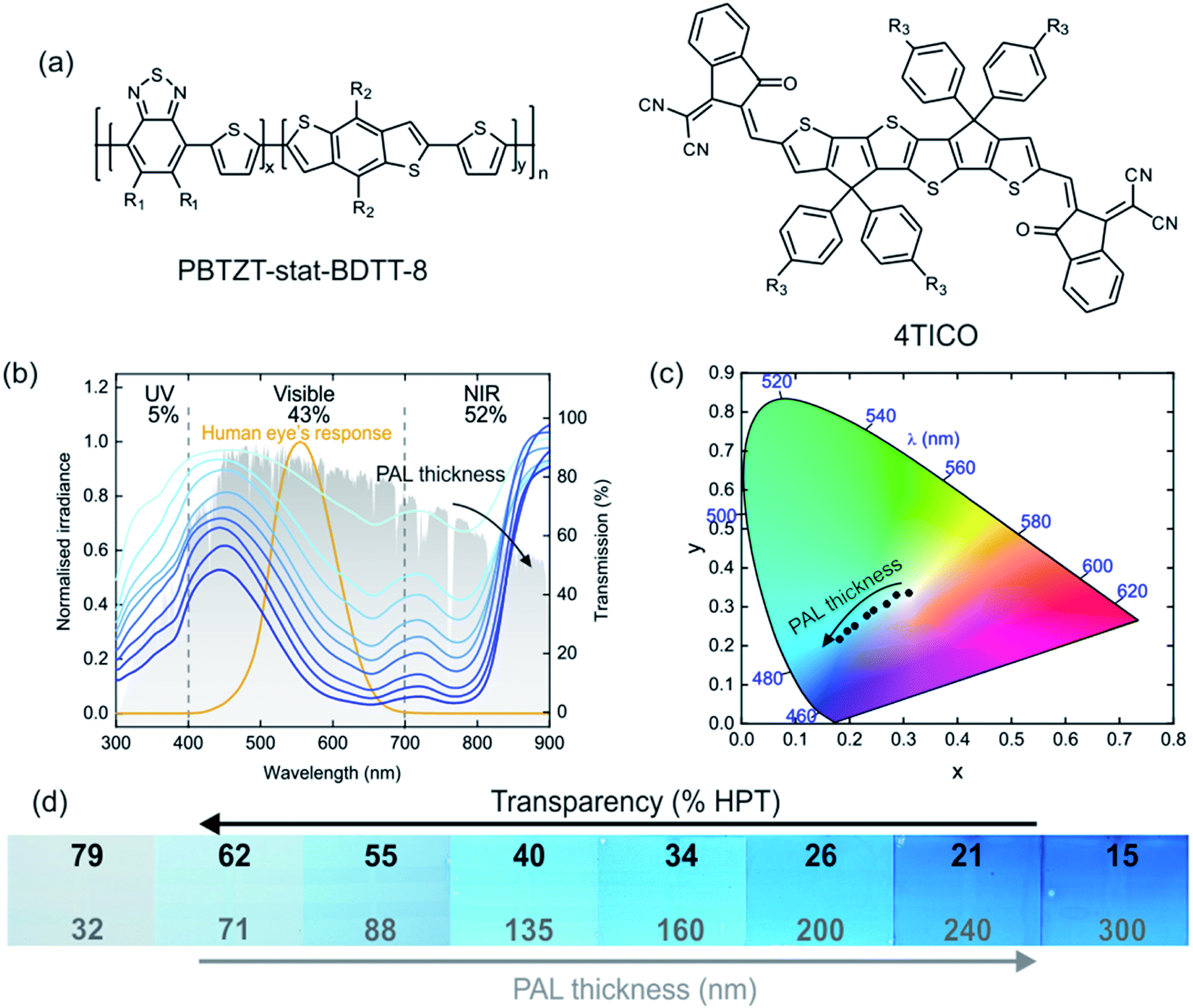 | ||
| Fig. 1 Photoactive layer (PAL) materials and optical properties. (a) Chemical structures of PBDTZT-stat-DBTT-8 and 4TICO. (b) Optical transmission of photoactive layers with different thicknesses. The percentage of irradiance in each of the three regions of the spectrum, ultraviolet (UV), visible and near infrared (NIR), indicated with the vertical dashed lines is given in the upper part of the plot. Normalised human eye's response and AM 1.5G spectra are also given. (c) Colour coordinates in transmission in CIE chromaticity diagram as a function of the thickness of the PBDTZT-stat-DBTT-8:4TICO blend. (d) Pictures of thin films with increasing thickness of the photoactive layer, labelled with the corresponding HPT values (top) and thickness (bottom). The size of each sample is 5 cm × 5 cm. | ||
Thickness measurements were done with a mechanical profilometer (Dektak XT 150). An optical microscope was used to measure the active area, the interconnection length and grooves features. Photoluminescence (PL), Raman scattering, and photocurrent maps of the module were measured using a WITec alpha 300 RA+ confocal setup. Two excitation solid-state lasers with central wavelengths of 488 nm (3 mW) and 785 nm (1 mW) were employed. Light beam induced current (LBIC) was measured simultaneously along with PL measurement/Raman using the same laser as the LBIC excitation source. Photocurrent maps were also collected using white light as excitation source, and the same piece of equipment (herein referred to as whiteBIC). The device photocurrent was acquired in short circuit conditions. As it was photogenerated, the signal was current–voltage amplified and then processed using WITec electronics through an auxiliary channel of the WITec current sensing module. The analysis was performed using the WITec Project FOUR software.
Results and discussion
Selection of photoactive materials
The choice of the organic semiconducting absorbers is crucial to achieve a high performance as well as other relevant aspects, including aesthetics, transparency and scalability (Table 1). In this study, the commercial PBTZT-stat-BDTT-8 (ref. 13 and 42) and 4TICO44 were selected as electron donor and acceptor materials, respectively, see Fig. 1(a).PBTZT-stat-BDTT-8 exhibits a great stability when blended with the fullerene derivative PCBM, and higher mobility compared to other polymeric donors.45 Indeed, this allows manufacturing devices with a relatively thick PAL (above 400 nm) while still retaining the device performance over 8%.13 As a matter of fact, this polymer has been intensively employed for large-scale demonstrators over 100 cm2.13,41
Despite the good transport properties of these fullerene-based blends, the fullerene acceptors barely contribute to the overall light absorption of the device, thus limiting the light-harvesting capacity of the system, and consequently the device performance. To partially overcome this limitation, we incorporate the newly developed non-fullerene acceptor 4TICO44 with the same core structure as the reported IHIC, that shows efficiencies over 9% when integrated in solar cells comprising evaporated electrodes.31 4TICO exhibits a strong absorption in the near-infrared (NIR) region and a weak absorption in the visible range, thus contributing to the transparency of the device (Fig. 1(b) and S2, ESI†). The optical transmission of the PBTZT-stat-BDTTT-8:4TICO photoactive layer with thicknesses ranging from 50 to 300 nm is shown in Fig. 1(b). The absorption spectra of the blend show the complementary optical contribution of both materials (Fig. S2, ESI†). While PBTZT-stat-BDTTT-8 absorbs light in most of the visible region from 300 to 700 nm, 4TICO exhibits a strong absorption from 600 to 900 nm with the maximum absorption in the NIR.
Colour and transparency
From the aesthetics perspective, one of the main advantages of using blends based on NFAs with strong near infrared absorption is that the colour (in the visible) is primarily defined by the polymeric material. The colour coordinates of the blend were calculated and plotted in the CIE chromaticity diagram shown in Fig. 1(c), taking into account the transmission spectra and an AM 1.5G light source from Fig. 1(b). The CIE colour coordinates of the photoactive layer materials are in good agreement with the pictures of the thin films (Fig. 1(d)), covering a wide range of the bluish area in the CIE chromaticity diagram. The colour coordinates of thinner films are located close to the centre of the chromaticity diagram, whereas those for thicker films shift towards the edge of the diagram. Additionally, the human perception transmittance (HPT, eqn (1)) considering simply the photoactive films was calculated as a function of the thickness varying from 80% to 15% for film thicknesses of 30 and 300 nm, respectively (Fig. 1(d)). Then, we calculated the deviation from those values considering all the layers of the device (Fig. S4, ESI†). Our data indicate that the colour is mainly defined by the PAL, with a minor influence of PEDOT 4083 and the ST top electrode.Adapting to printing industry requirements
The next stage in the transition towards the integration of PBDTZT-stat-DBTT-8 and 4TICO as a potential system in BIPV is to adapt the manufacturing process to the industry requirements, here defined in Table 3.11,46–48 With that purpose, only large-scale compatible techniques were employed in this work.49 In particular, the charge transport layers, PAL and semitransparent top-electrode were likewise blade-coated. Additionally, all layers were processed in air, thus reducing the overall cost of the printing process and avoiding the use of a controlled atmosphere, otherwise frequently required for casting top-performing OPVs.50–52 Another critical aspect in order to meet industrial printing regulations32,53 is to avoid the use of harmful and hazardous halogenated solvents. Both the PBDTZT-stat-DBTT-8 polymer and the 4TICO acceptor were originally designed and synthesised to be efficient, soluble and processable in non-halogenated solvents such as o-xylene.53,54 Finally, for an easy lab-to-fab transfer the processing temperature should not exceed 150 °C in plastic flexible substrates, although in rigid substrates can be higher due to the good thermal stability of these semiconductor materials.13 In this work, the highest casting and annealing temperatures were 65 °C and 140 °C, respectively.| Item | Target |
|---|---|
| Coating technique | Scalable such as slot-die or blade coating |
| Casting atmosphere | In air |
| Top electrode | Solution processing |
| Formulation | Non-halogenated solvents |
| Processing temperature | <150 °C |
| Photoactive layer thickness | Insensitive/high tolerance |
Solution-processed semitransparent and opaque devices
The transition from opaque to fully solution-processed semitransparent devices requires finding efficient and solution-process electrode alternatives to the evaporated silver electrode. Fig. 2(a) depicts the inverted architecture of the devices for both opaque, used as reference, and semitransparent (ST) electrodes. In our study, highly conductive PEDOT:PSS (PH1000) was selected due to its good balance between electrical conductivity and transparency.8,32 Furthermore, PH1000-based electrode is metal-free and can be processed from solution as the rest of the layers.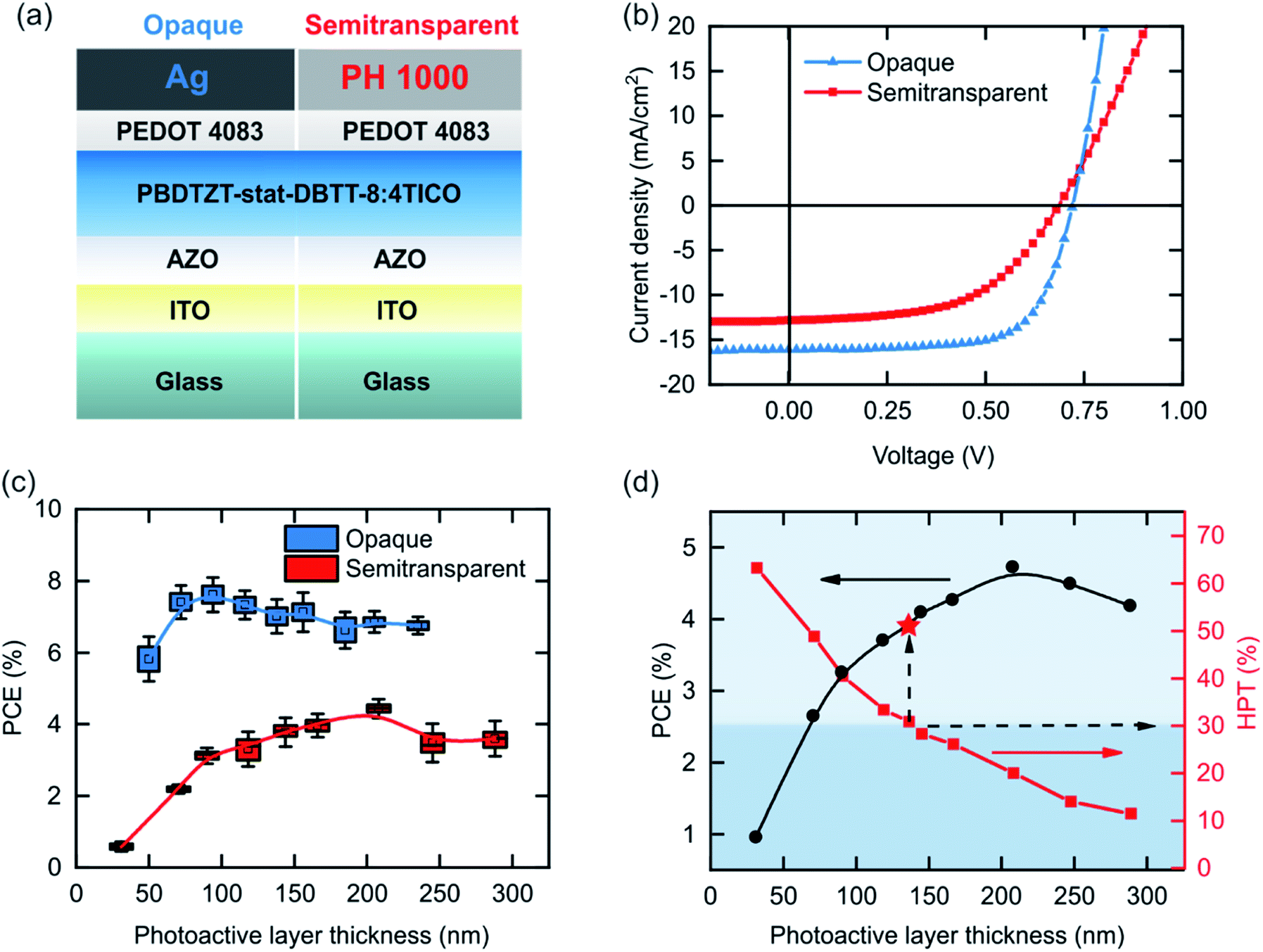 | ||
| Fig. 2 Opaque and semitransparent (ST) individual solar cell devices. (a) Sketch of the device architectures and (b) JV characteristics for both opaque and ST devices. (c) Power conversion efficiency (PCE) as a function of the active layer thickness. Box whiskers represent 1st and 3rd quartile. (d) PCE (left axis) and human perception transmittance (HPT, right axis) of the full stack for the best ST devices as a function of the photoactive layer thickness. | ||
Fig. 2(b) shows the best JV curves for both opaque and ST devices, see also Table 4. The optimum PAL thickness (Fig. 2(c) and Table 4) is mainly governed by the trade-off between fill factor (FF) and short-circuit current (Jsc), having a minor effect the reduction in the open-circuit voltage (Voc). Whereas the opaque electrode yields mean values of FF of 68.7% and a Jsc of 16.5 mA cm−2, the ST devices reach 48.2% and 13.3 mA cm−2, respectively. Comparing the relative performance between the two device configurations, FF and Jsc drop 30% and 20%, respectively, when moving from opaque to ST electrodes. This 30% drop in FF is ascribed to the combination of three factors.
| Electrode | V oc (V) | J sc (mA cm−2) | FF (%) | PCE (%) | PAL thickness (nm) | HPT (%) |
|---|---|---|---|---|---|---|
| Opaque | 0.72 ± 0.01 (0.72) | 16.5 ± 0.6 (16.1) | 68.7 ± 0.1 (68.8) | 7.6 ± 0.3 (8.0) | 95 | 0 |
| Semitransparent | 0.69 ± 0.01 (0.69) | 13.3 ± 0.3 (12.9) | 48.2 ± 2.8 (53.3) | 4.4 ± 0.2 (4.7) | 200 | 20 |
(i) Thicker OPV films tend to inherently have lower FF, especially in systems with limited mobility, since charge recombination processes are more likely to happen before charge collection occurs. Despite the moderately high mobility of the polymer,45 this effect is non-negligible in the resulting optimum PAL thicknesses around 100 nm for opaque devices in contrast with the 200 nm for ST devices. Additionally, the replacement of fullerene derivatives with NFAs might also limit the mobility in the PAL.55 (ii) The lack of back reflection in the top electrode. The evaporated silver electrode introduces an optical enhancement effect in the opaque devices. Incoming light is multiple-times absorbed in the PAL due to the reflection at the mirror-like silver layer, thus enhancing the overall absorption in the PAL. In ST devices, in contrast, the lack of back reflection has to be compensated with an increase of the absorber layer, unavoidably sacrificing FF. (iii) The conductivity of the top electrode influences the charge collection efficiency. In our particular case, there are three orders of magnitude difference between the electrical conductivity of PH1000 (104 S m−1) and evaporated silver (107 S m−1).56 In a previous work, the effect of the resistance introduced by the electrical conductivity of the ST electrode material was estimated to be over 70% of the electrical losses.32 In our work, the overall efficiency dropped from 7.6% to 4.4% when replacing the opaque electrode with the ST counterpart. It is worth highlighting that an equivalent drop in efficiency (from 6% to 3.8%) was recently reported using the same polymer, PBDTZT-stat-DBTT-8 blended with a fullerene acceptor.57 In that case, silver nanowires (Ag NW) embedded in a matrix of PEDOT:PSS were used as the ST top electrode. However, this strategy did not reduce the drop in Jsc and FF. Alternatively, replacing PH1000 with a pristine film of Ag NW on top of PEDOT:PSS was reported to potentially improve the electrical conductivity by one order of magnitude, yet retaining the transparency of the device.20,58 It is thus clear that further investigations on highly conductive ST electrodes are required in order to mitigate this drop in performance.
Ideally, one of the prerequisites for a potentially scalable OPV system is thickness-performance insensitivity to minimise the drop in performance upon the intrinsic thickness variations of the large-scale printing techniques (cf. slot-die).59 In order to evaluate this feature in the proposed PBDTZT-stat-DBTT-8:4TICO system, devices with different thicknesses of the PAL ranging from 50 to 250 nm were manufactured (Fig. 2(c) and S1, ESI†). Opaque devices within a broad range of thicknesses, between 100 and 250 nm, surpass 7% of PCE. This minor thickness dependence indicates that PBDTZT-stat-DBTT-8:4TICO is a suitable system for upscaling. We calculated the HPT of ST cells as a function of the photoactive layer thickness (see Fig. 2(d)). As expected, the HPT decreases inversely proportional with the thickness of the PAL.
Considering the target HPT value for BIPV (transmittance ≥30%, Table 1) and our results, the studied OPV system could deliver performances over 4.1%.
Although the highest performing ST devices are based on 200 nm thick films, the HPT of those films is 20%, which is below the target 30% HPT (see HPT values of full devices in Table S2, ESI†). Consequently, the maximum photoactive layer thickness was reduced down to 135 nm in our subsequent experiments. In our approach, the device transparency is mainly governed by the PAL followed by PH1000 layer and, in a minor proportion, by PEDOT 4083, ITO and ZnO, see (Fig. S3, ESI†). More details about the individual contribution of each semitransparent layer can be found in Table S2 (ESI†).† We believe that the efficiency for a given transparency level could improve further by engineering the top electrode with a higher degree of transparency and more electrically conductive ST materials.
Laser-patterned OPV modules
The upscaling study towards ST modules was performed using the same optimised stack for ST lab cells (ITO/AZO/PAL/PEDOT 4083/PH1000). The module prototype consists of 3 or 4 individual cells that are monolithically interconnected in series, with an area of around 1 cm2 (the exact value depends on the cell length, Lcell, and the number of connected cells, Ncell, Fig. 3). Fig. 3(a) shows a schematic cross-section diagram of the module design shown in Fig. 3(b). With this design, either 2 or 4-subcell modules can be measured independently, thus enabling a more flexible assessment of the performance. For the monolithic interconnection, sequential laser ablation and coating steps are required, in particular, ITO/[P1]/AZO/PAL/PEDOT4083/[P2]/PH1000/[P3]. The laser ablation was carried out using an industrially compatible laser equipment with 1064 nm excitation and a minimum pulse width of 1 μs. In order to minimise the patterned width and, thus, the length of the interconnection between cells (Li), a comprehensive optimisation of the laser parameters was carried out (see Table S1, ESI†). P1 is the least critical patterning step since there is no sensitive layer underneath (glass substrate). P1 groove aims to electrically isolate ITO stripes, see Fig. 3(a). The efficacy of the ITO ablation was validated by means of profilometry (Fig. S5, ESI†) and by measuring an electrical resistance over 15 MΩ between adjacent ITO stripes. Additionally, the resulting groove after the P1 patterning was evaluated with photoluminescence (PL) and light reflection maps (Fig. S6, ESI†). A high enough laser power fully removes the ITO, as shown in the PL and reflection maps (Fig. S6(b, c, e and f), ESI†). In contrast, when the laser power is too low, an incomplete ITO removal is obtained (Fig. S6(a and d), ESI†). Interestingly, the reflection maps reveal higher ITO signal at the edges of the grooves than in the central part. This correlates with the presence of spikes at the edge of the groove as a result of the ablation of ITO, as observed in the measured profiles.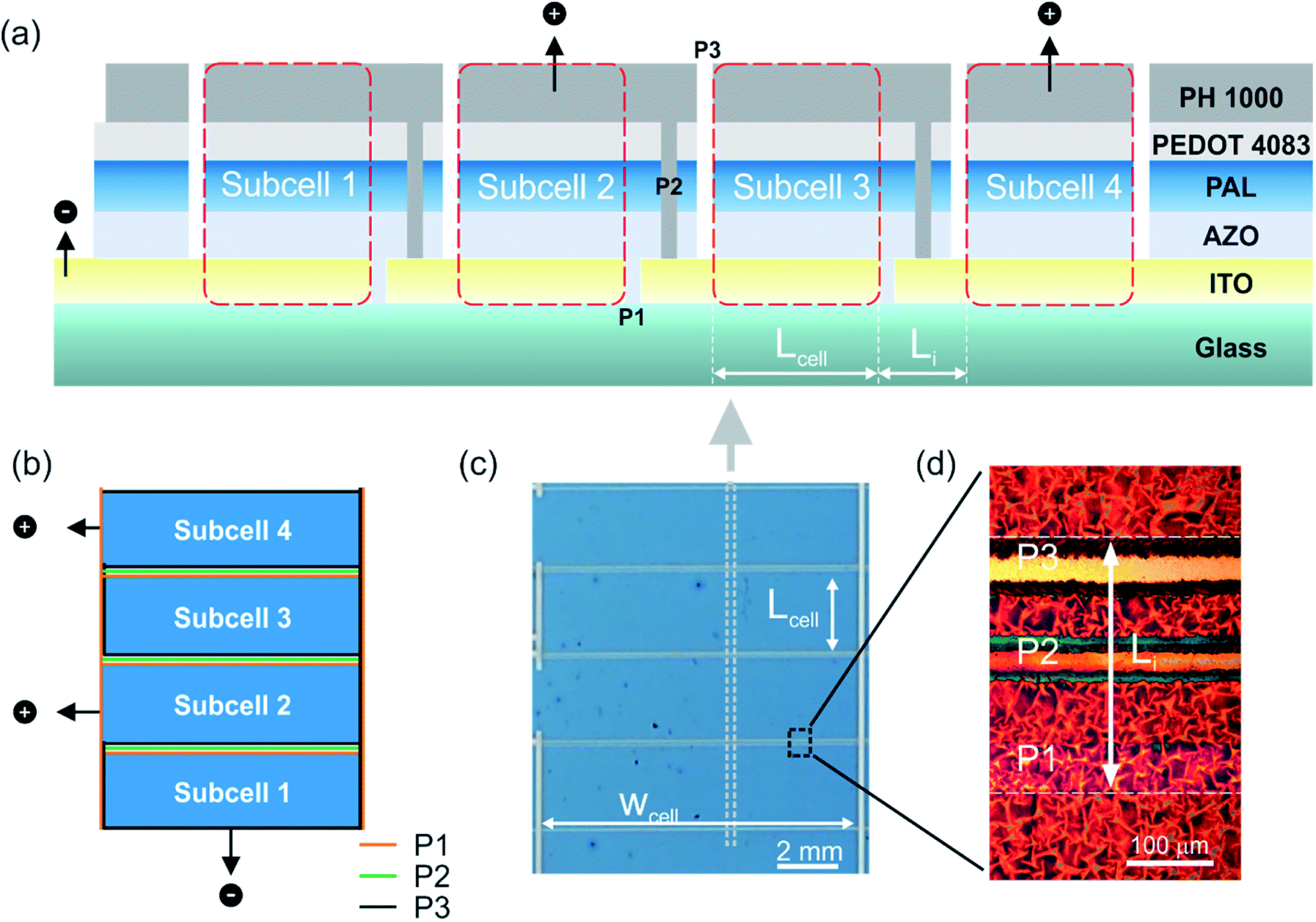 | ||
| Fig. 3 Laser-patterned modules. General schemes of the (a) cross-section and (b) top-view of a 4 monolithically interconnected (P1–P2–P3) subcells in a module (further details of the layout of modules are in Fig. S5, ESI†). (c) Top view photograph of a module with 4 subcells connected in series. (d) Microscope image of the module interconnection P1–P2–P3. | ||
The height of those spikes, however, does not exceed 40 nm, and hence they are expected to be fully covered by the AZO layer (which has a nominal thickness of 40 nm), Fig. S5, ESI.† P2 and P3 patterning steps, however, are more challenging than P1, as they require a precise ablation of the target layers without damaging the ITO underneath, which would reduce drastically the module performance. The P2 ablation step provides a path for the interconnection of the top and bottom electrode, accomplished upon PH1000 coating, see Fig. 3(a). Finally, P3 is equivalent to P1 but electrically disconnecting the top electrode, intending to define the individual subcells. The optimised width of the patterned grooves (Fig. S7, ESI†) for P1, P2 and P3 were 65 μm, 51 μm and 74 μm, respectively.
The interconnection length (Li, see Fig. 3(a)), when multiplied by the width of the module results in the so-called dead area, accounts for the distance between the P1 and P3 resulting grooves. Despite not using an optically assisted nor a XY motorised positioning system, a remarkable interconnection length of 300 μm was achieved, benchmarking with the results obtained when using femtosecond lasers (Fig. 3(c)).20 This low interconnection distance is crucial to achieving modules with high geometrical fill factor (GFF).
Co-local optoelectronic characterisation
To assess the module interconnection and the ST module performance, advanced optoelectronic measurements of the module were carried out. More precisely, simultaneous Raman spectra and laser-beam-induced-current (LBIC) maps were acquired at 488 nm excitation wavelength in order to correlate the electrical performance with the film morphology.60 Additionally, photoluminescence (PL) and LBIC maps were also acquired at 785 nm excitation wavelength. Due to the complementary absorption of the PAL materials, co-local maps measured at 488 nm correspond mainly to the PBDTZT-stat-DBTT-8 contribution, whereas 785 nm maps correspond to photocurrent produced by light absorbed by 4TICO.To facilitate the analysis of the co-local measurements, the scanned area in Fig. 4 is divided into five different areas in one individual subcell of the module. (1) full cell stack but electrically disconnected from the subcell, (2) P3 groove defining the start of the photoactive area, (3) photoactive area of the cell also known as subcell, (4) cell-to-cell interconnection (P1, P2, P3) and (5) full stack of photoactive material belonging to the following subcell, equivalent to (3) but not evaluated in this measurement.
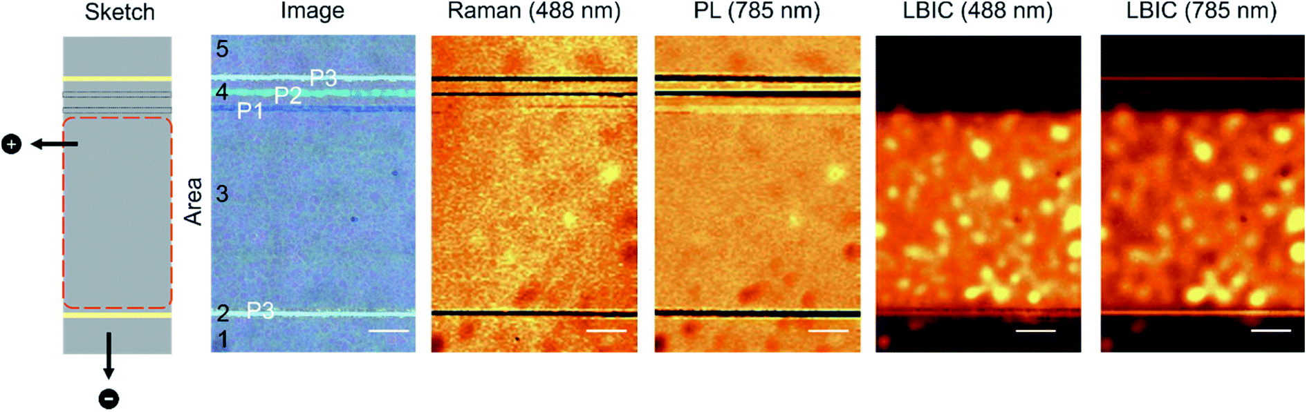 | ||
| Fig. 4 Advanced co-local optoelectronic characterisation of a module subcell at different wavelengths. (from left to right) Top view sketch, optical image, Raman map excited at 488 nm, PL map excited at 785 nm, LBIC map at 488 nm and 3 mW, and LBIC map at 785 nm at 1 mW. Area legend in optical image: (1) and (5) non-connected part of the subcell, (2) P3, (3) active area of the subcell and (4) cell interconnection (P1, P2, P3). Scale bar corresponds to 300 μm. | ||
Areas 1 and 5 have the same layered stack as the rest of the module (Raman and PL maps) although both areas are electrically disconnected from the investigated central cell, as confirmed by the negligible electrical signal of LBIC maps in both areas. The P3 groove (Area 2) disconnects electrically Areas 1 and 3. Thus, it defines one edge of the active area removing the top electrode material, see Fig. 3(a). The Raman and PL signals in Area 2 are dramatically low compared to the rest of the module, proving not only an effective PH1000 removal but also the ablation of the PAL. Surprisingly, the electrical contribution of P3 (Area 2) is not as low as one would theoretically expect, as seen in the LBIC maps. This current enhancement is believed to be an artefact of the measurement originated from scattered light at the rough interconnect which might even waveguide light into the neighbouring PAL (note that at those loci there is no photoactive material underneath). The quality of P3 removal is also shown in the top groove (P3) of Area 4 exhibiting the same features as P3 in Area 2. This finding indicates a reproducible laser patterning procedure. In Area 3, which corresponds to the active area of the subcell, Raman and PL maps show a rather homogenous distribution of photoactive material with no significant thickness variations derived from the blade-coating process. Both the Raman map and the optical image depict a similar granulated texture appearance. We attribute this to a morphological effect of the PH1000 top electrode rather than to the contribution of the photoactive layer since this texture is not visible in the PL map, and thus is not related to absorption or other optical effects. Besides, this is supported by the magnified optical microscope image in Fig. 3(d), which reveals the crystal-like structure of PH1000. Additionally, the darker spots in both Raman and PL maps may suggest small thickness reduction leading to lower Raman and PL intensities. These thinner aggregates are well correlated with the higher photocurrent measured in the LBIC maps.
Note that both LBIC photocurrent maps (at 488 nm and 785 nm) have the same features, exhibiting the maximum and minimum performance points at the same positions (Fig. 4) thus revealing a similar donor and acceptor contribution. The complete monolithic subcell-to-subcell module interconnection (Area 4, P1–P2–P3) is easily distinguishable by the 3 parallel grooves. The P1 patterning removes the ITO and is followed by the coating of the ETL/PAL/HTL layers, hence the PL and Raman signals. This, however, is slightly lower than in the rest of the image due to the reduced back reflection from the glass compared to the ITO layer. Additionally, P1 delimits the photocurrent generation area (see LBIC maps in Fig. 4). The absence of signal from the photoactive materials in the Raman and PL maps in Area 4 proves the success of P2 and P3 patterning. The small contribution in P2 and P3 observed in the 785 nm LBIC map is ascribed to light scattering (see above). These results confirm that the laser patterning of the module interconnection was satisfactorily performed, leading to a well-defined active area of the subcells. Finally, we evaluated the optimised laser patterning conditions upon thickness variations in P2, the most sensitive patterning step. Fig. S8 (ESI†), depicts the satisfactorily patterned PAL films of 80 nm, 120 nm (reference) and 140 nm using the same laser parameters described in Table S1 (ESI†). Although the groove width is smaller for the thicker film compared with the thinner film, the modules work in the whole studied PAL thickness range. This reveals that the optimised patterning conditions are also thickness insensitive and modules with thickness variations of 50 nm in the PAL can be successfully patterned.
Geometrical parameters of modules
Once we validated the laser patterning process and the module operation, we explored ways to maximise the geometrical fill factor (GFF). Three relevant geometrical parameters directly influence the GFF of the module (see Fig. 3 and eqn (3)), namely the cell length (Lcell), the interconnection length (Li) and the number of the interconnected cells (Ncell), see the geometrical definition in Fig. 3. Note that the GFF is independent of the cell width (wcell), since the only relevant geometrical parameters are those sensitive to the charge transport direction within the PAL (Lcell and Li). On the other hand, wcell directly influences the active area size of the device. Consequently, a simple and effective strategy to increase the active area of the module without affecting the rest of the geometrical parameters and charge transport is to increase the cell width (wcell). To assess the module Lcell-performance sensitivity for the chosen ST electrode, ST modules of 2 mm, 3 mm and 4 mm of Lcell were manufactured.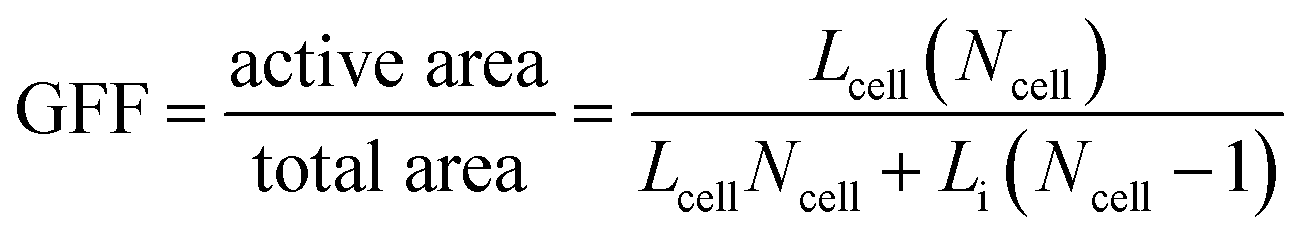 | (3) |
Table 5 shows the influence of Lcell on the photovoltaic performance parameters. The Voc values of the modules are proportional to the number of series interconnected cells and do not depend on the length of the subcell, as expected, thus indicating an efficient laser patterning. On the one hand, a small reduction in the Jsc (<1 mA cm−2) is observed when Lcell is increased from 2 to 4 mm. Interestingly, when comparing modules with lab cells, the Jsc values are not affected (11.1 mA cm−2) when increasing the active area from 0.08 cm2 (cell) to 1.1 cm2 (largest module).
| L cell (mm) | N cell | V oc-module (V) | V oc-subcell (V) | I sc-module (mA) | J sc-subcell (mA cm−2) | FF (%) | PCE (%) | GFF (%) | HPT (%) | AAmodule (cm2) | |
|---|---|---|---|---|---|---|---|---|---|---|---|
| a AAmodule corresponds to the active area of a single cell. b Refers to individual assessment of JV curves from Fig. 6(a). | |||||||||||
| Modules | 2 | 4 | 2.88 ± 0.02 (2.88) | 0.72 ± 0.01 (0.72) | 1.95 ± 0.05 (1.98) | 10.9 ± 0.3 (11.1) | 50.2 ± 0.3 (51.5) | 3.9 ± 0.1 (4.1) | 87.6 | 34.6 | 0.71 |
| 3 | 4 | 2.89 ± 0.03 (2.89) | 0.73 ± 0.01 (0.72) | 3.11 ± 0.10 (3.24) | 11.3 ± 0.4 (11.8) | 44.8 ± 0.3 (45.7) | 3.8 ± 0.1 (3.9) | 92.2 | 34.7 | 1.10 | |
| 4 | 3 | 2.18 ± 0.02 (2.19) | 0.72 ± 0.01 (0.72) | 3.72 ± 0.05 (3.70) | 10.3 ± 0.4 (10.3) | 43.7 ± 0.3 (45.5) | 3.3 ± 0.1 (3.4) | 93.2 | 35.2 | 1.01 | |
| Subcells | 2b | 2b | 1.45b | 0.73b | 2.4b | 11.8b | 47.3b | 4.1b | 84.7b | 30.2b | 0.397b |
| 2b | 4b | 2.81b | 0.70b | 2.4b | 12.0b | 48.7b | 4.1b | 84.7b | 30.2b | 0.794b | |
| Ref. | 1 | — | 0.69 ± 0.05 (0.69) | — | 11.1 ± 0.4 (11.1) | 50.5 ± 2.8 (53.4) | 3.9 ± 0.2 (4.1) | — | 33.4 | 0.08a | |
On the other hand, the 2 mm-Lcell module shows the highest FF (50.2%), similar to the single devices (50.5%), whereas it is reduced to 45.5% in the 3 mm and 4 mm counterparts (Fig. S9, ESI†). This important FF-Lcell dependence is expected as the transport path increases with Lcell. This transport-related limitation could be diminished by enhancing the electrical conductivity of the electrodes, which would allow a further Lcell increase, thus improving the GFF of the module. Considering that the sheet resistance of the top electrode PH1000 is 20 times higher than the bottom ITO electrode, the performance-geometry dependence points to the limited conductivity of PH1000 as the bottleneck for the upscaling of this system.32
Finally, the overall module PCE is not as sensitive as the FF-Lcell dependence, since an average performance over 3.8% is achieved for 2 and 3 mm-Lcell modules. However, the performance of the 4 mm-Lcell modules drops to 3.3%. Remarkably, ST single cells and 2 and 3 mm-Lcell modules yield similar performances despite a 9 and 14-fold active area (AAmodule) increase, respectively, compared to single-cells. Consequently, this study allows us to define the cell dimensions so that the module design has a negligible impact on the PCE.
Geometry optimisation by co-local characterisation techniques
In order to have a better understanding of the Lcell-PCE dependence, we studied the 2, 3 and 4 mm-Lcell modules by means of co-local optoelectrical imaging (Fig. 5). For the sake of the visualisation of the micron-sized features, we assessed only one of the subcells of the module, as it was done in Fig. 4, taking advantage of the flexibility of the module layout (Fig. S10, ESI†). In particular, we acquired maps of the PL and LBIC, together with the photocurrent map using the microscope white light as illumination source, aka whiteBIC. In contrast to LBIC, whiteBIC is a panchromatic technique, therefore the overall photocurrent contribution from the two photoactive materials is measured at the same time. Additionally, it allows determining the active area of the module without scattering artefacts. Indeed, using broadband light excitation, the whiteBIC technique does not generate scattered light and light guiding effects at the patterned grooves (see LBIC maps in Fig. 4 and 5) owing to the larger spot size of the light beam and the larger focal lengths with different wavelengths.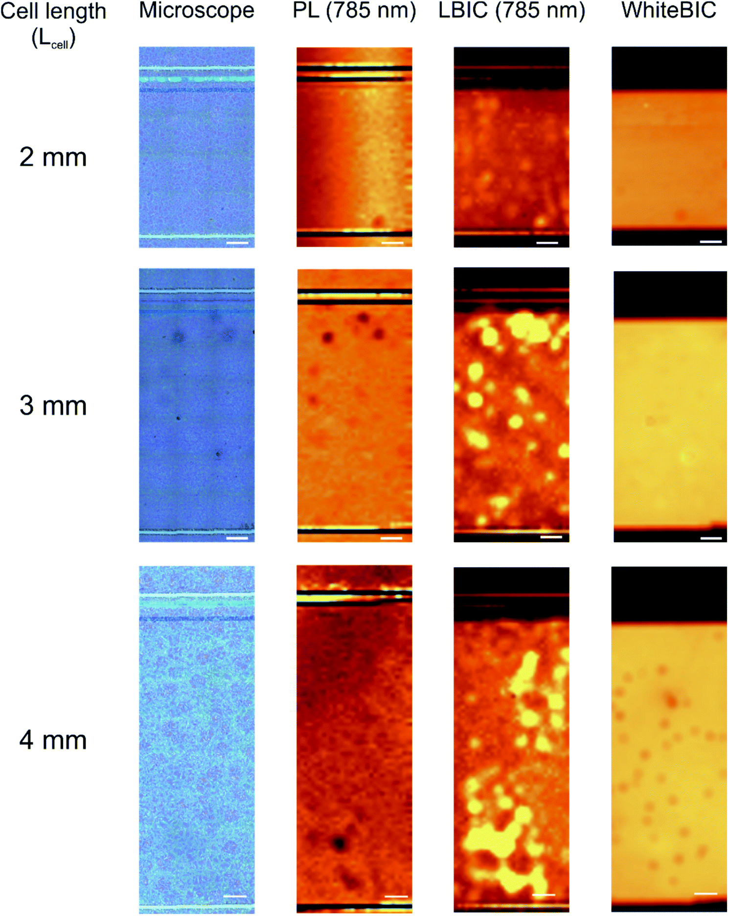 | ||
| Fig. 5 Geometry optimisation via co-local electrical and optical mapping. Microscope image, photoluminescence (PL), laser-beam induced-current (LBIC) excited at 785 nm and with white light LBIC (aka whiteBIC) maps (columns from left to the right) of laser-patterned modules with cell lengths of 2, 3 and 4 mm (rows up to down). The white scale bar corresponds to 300 μm. The scanned width (Wcell) was in all cases 1.6 mm. LBIC maps are normalized respect to the 3 mm-Lcell module. | ||
To extend the analysis of the co-local maps in the charge transport direction, Fig. S11 (ESI†) shows the averaged cross-section along the Lcell of each of the maps extracted from Fig. 5. The co-local maps have some features in common for all cell lengths of the module.
First, despite the large variations of Lcell, there is no photocurrent drop along the whiteBIC cross-section images (Fig. S11, ESI†). The homogenous distribution of the photocurrent throughout the Lcell suggests insensitive charge collection in this module geometry. Second, the black parallel lines at the top of the PL maps in Fig. 5 are an indication of an efficient patterned P2 and P3 grooves. This proves the reliability and reproducibility of the patterning process regardless of the module design. Third, the aggregates observed in the PL maps (darker spots) are well correlated with areas of higher photocurrent in the 785 nm LBIC maps but not in the whiteBIC maps. This could be partially attributed to scattered laser light (defects) since some of the spots are well correlated with dark spots in the microscope image. However, these areas do not have a detrimental effect on the whiteBIC maps. Note that, the whiteBIC maps also reveal a reduction of the performance at the edge of the PAL. As it can be identified in the P3 groove in Fig. 3(b), this is caused by the burning of the organic material around the edges upon laser patterning. This effect is also visible in the PL maps of Fig. 5 as well as in the peaks of the PL cross-section (Fig. S11, ESI†), associated with a higher PL signal at the groove edges. However, this small reduction of the effective Lcell of less than 20 μm is negligible since it corresponds to an area loss of only 2.3% in the case of 3 mm-Lcell modules. On the other hand, there are also some differences depending on the cell length. For the 2 mm-Lcell modules, both PL and 785 nm LBIC map cross-section show very smooth and flat characteristics (Fig. S11, ESI†) revealing a homogenous coating distribution of the photoactive material. The profiles are less smooth for the 3 mm and 4 mm cells. The 3 mm-Lcell module exhibits the highest whiteBIC signal (Fig. S11, ESI†), in agreement with the photovoltaic parameters in Table 5, closely followed by the 4 mm-Lcell modules. To sum up, we confirmed the great potential of the use of co-local, non-invasive imaging techniques for the characterisation and optimisation the ST laser patterned modules. More specifically, this module design yields over 90% of GFF while at the same time exhibiting a 34% HPT. Overall, the performance of the ST modules (3.8%, over 1.1 cm2) is as good as in small ST devices (3.9%, 8 mm2). This confirms that the developed laser patterning process is a fully compatible technique for upscaling the OPV solar cells.
Hereafter we analysed the effect of the number of the subcells on the module. The flexible design of the module layout, shown in Fig. S10 (ESI†), enables accessing independently the desired number of interconnected subcells. Fig. 6(a) depicts the JV characteristics of a 2-subcell and 4-subcell module (Table 5). The invariability of the Jsc with the number of the interconnected subcells is a further confirmation that the accurate laser patterning provides an efficient interconnection. The Voc of the ST module (Table 5) also scales linearly with the number of the connected subcells (depending on the design 3 or 4 subcells). This result is a relevant milestone in the upscaling of this OPV system, as it suggests that the performance of the module can be maintained upon increasing the active area size with a suitable module design. In particular, the record efficiency of the module shown in Fig. 6(a) is 4.1% for both the 2 and 4 interconnected subcells. Besides the performance, the ST module exhibits a high degree of transparency (Fig. 6(b)). Noteworthy the 3 interconnection regions, with a width of 300 μm each, are hardly visible by the naked eye in our ST module. This is an intrinsic advantage of laser patterned ST modules over those fabricated solely by means of slot-die coating and screen printing, where the individual interconnections can be easily noticeable.
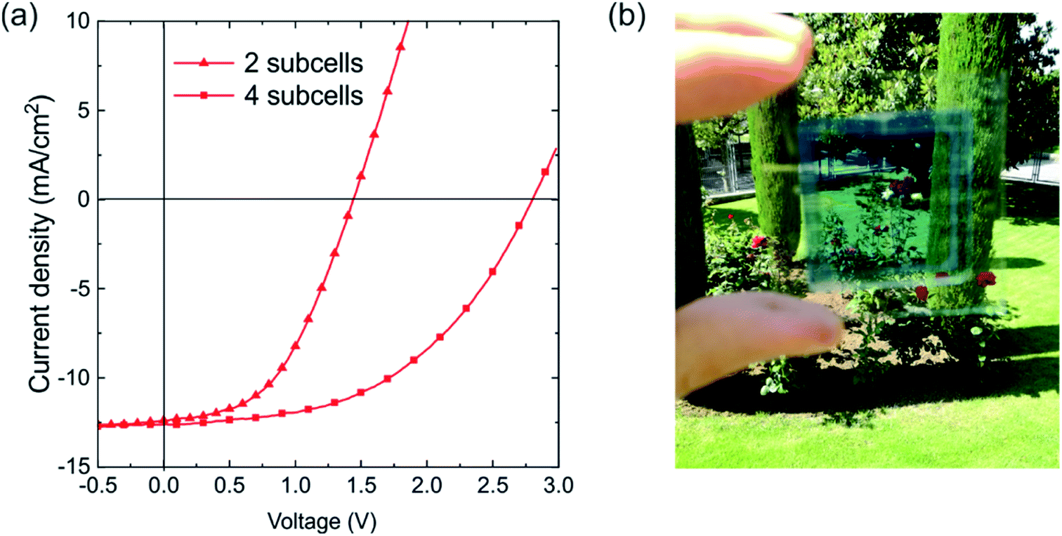 | ||
| Fig. 6 Semitransparent module. (a) JV characteristics of 2 and 4 subcells interconnected in series, corresponding to half a module and a full module, respectively. (b) Photograph of a semitransparent sample containing four OPV modules based on PBDTZT-stat-DBTT-8:4TICO. | ||
Conclusions
Organic photovoltaics are expected to become an important player in the BIPV market, especially in applications that require a high transparency such as photoactive windows. Based on our experience with customers, we propose those specific characteristics that an OPV system has to fulfill, including a transmission equivalent higher than 30% HPT and appealing colours for architecture, such as blue, green or grey. In this work, we have studied the candidate system comprising the semiconducting blue polymer PBDTZT-stat-DBTT-8 and the strong NIR absorbing acceptor 4TICO. The fabrication of the solar cells and modules has been carried out following industrial preferences for low embodied energy technologies including air processing, full solution-process from non-halogenated formulations, low annealing temperatures and no evaporation steps. Despite the high transmittance required, which limits the light-harvesting capacity, the fabricated semitransparent modules yield around 4% efficiency, with a geometrical fill factor above 90% and 1 cm2 active area. Importantly, the system shows a negligible drop in performance upon area scaling from 8 mm2 to 1.1 cm2. Moreover, a laser patterning process has been implemented in the fabrication of the modules to narrow the interconnection length down to 300 μm.A comprehensive characterisation of the modules has been done with the aid of advanced co-local optical and electrical imaging techniques, namely laser-beam/white-light induced photocurrent and, photoluminescence and Raman scattering mapping. These techniques have helped to correlate the local morphological features of material with the photocurrent distribution as well as to validate the efficacy of the laser patterning. On the other hand, the moderate module efficiency suggests room for improvement, being the semitransparent top electrode the bottleneck for achieving higher performances over larger areas. Yet, the results of this work encourage the use of organic semiconductors with strong absorption in the infrared as key materials for the photoactive architectonic elements of the future.
Conflicts of interest
There are no conflicts to declare.Acknowledgements
This work was supported by the Spanish Ministerio de Economía y Competitividad (MINECO) under Grant PGC2018-095411-B-I00 and No. SEV-2015-0496 in the framework of the Spanish Severo Ochoa Centre of Excellence and by EURECAT Technological Centre. We acknowledge financial support from European Research Council through project ERC CoG 648901 and H2020 Marie Curie actions through the SEPOMO project (Grant number 722651). E.P.-S.-J. wants to thank Mr Pierluigi Mondelli for his help in the laser patterning experimental setup and Mrs Léa Silvestre for her help manufacturing devices. We acknowledge support of the publication fee by the CSIC Open Access Publication Support Initiative through its Unit of Information Resources for Research (URICI).References
- I. Cerón, E. Caamaño-Martín and F. J. Neila, Renewable Energy, 2013, 58, 127–133 CrossRef.
- K. Jeong, T. Hong, C. Koo, J. Oh, M. Lee and J. Kim, Appl. Sci., 2017, 7, 1077 CrossRef.
- D. Shin and S.-H. Choi, Coatings, 2018, 8, 329 CrossRef.
- C. J. M. Emmott, J. A. Röhr, M. Campoy-Quiles, T. Kirchartz, A. Urbina, N. J. Ekins-Daukes and J. Nelson, Energy Environ. Sci., 2015, 8, 1317–1328 RSC.
- Y. Cui, Y. Wang, J. Bergqvist, H. Yao, Y. Xu, B. Gao, C. Yang, S. Zhang, O. Inganäs, F. Gao and J. Hou, Nat. Energy, 2019, 4, 768–775 CrossRef CAS.
- D. Chemisana, A. Moreno, M. Polo, C. Aranda, A. Riverola, E. Ortega, C. Lamnatou, A. Domènech, G. Blanco and A. Cot, Renewable Energy, 2019, 137, 177–188 CrossRef.
- J. Hou, O. Inganas, R. H. Friend and F. Gao, Nat. Mater., 2018, 17, 119–128 CrossRef CAS PubMed.
- S. Dai and X. Zhan, Adv. Energy Mater., 2018, 8, 1800002 CrossRef.
- J. Yuan, Y. Zhang, L. Zhou, G. Zhang, H.-L. Yip, T.-K. Lau, X. Lu, C. Zhu, H. Peng, P. A. Johnson, M. Leclerc, Y. Cao, J. Ulanski, Y. Li and Y. Zou, Joule, 2019, 3, 1140–1151 CrossRef CAS.
- N. Li, I. McCulloch and C. J. Brabec, Energy Environ. Sci., 2018, 11, 1355–1361 RSC.
- I. Burgués-Ceballos, M. Stella, P. Lacharmoise and E. Martínez-Ferrero, J. Mater. Chem. A, 2014, 2, 17711–17722 RSC.
- Q. Liu, Y. Jiang, K. Jin, J. Qin, J. Xu, W. Li, J. Xiong, J. Liu, Z. Xiao, K. Sun, S. Yang, X. Zhang and L. Ding, Sci. Bull., 2020, 65, 272–275 CrossRef.
- S. Berny, N. Blouin, A. Distler, H. J. Egelhaaf, M. Krompiec, A. Lohr, O. R. Lozman, G. E. Morse, L. Nanson, A. Pron, T. Sauermann, N. Seidler, S. Tierney, P. Tiwana, M. Wagner and H. Wilson, Adv. Sci., 2016, 3, 1500342 CrossRef PubMed.
- R. Xue, J. Zhang, Y. Li and Y. Li, Small, 2018, 14, 1801793 CrossRef PubMed.
- J. Halme and P. Mäkinen, Energy Environ. Sci., 2019, 12, 1274–1285 RSC.
- E. Pascual-San José, A. Sánchez-Díaz, M. Stella, E. Martínez-Ferrero, M. I. Alonso and M. Campoy-Quiles, Sci. Technol. Adv. Mater., 2018, 19, 823–835 CrossRef.
- E. Pascual-San-José, X. Rodríguez-Martínez, R. Adel-Abdelaleim, M. Stella, E. Martínez-Ferrero and M. Campoy-Quiles, J. Mater. Chem. A, 2019, 7, 20369–20382 RSC.
- L. Wen, Q. Chen, F. Sun, S. Song, L. Jin and Y. Yu, Sci. Rep., 2014, 4, 7036 CrossRef PubMed.
- K. Forberich, F. Guo, C. Bronnbauer and C. J. Brabec, Energy Technol., 2015, 3, 1051–1058 CrossRef CAS.
- S. Strohm, F. Machui, S. Langner, P. Kubis, N. Gasparini, M. Salvador, I. McCulloch, H. J. Egelhaaf and C. J. Brabec, Energy Environ. Sci., 2018, 11, 2225–2234 RSC.
- J. L. Caivano, Color Res. Appl., 2006, 31, 350–363 CrossRef.
- W. van Sark, P. Moraitis, C. Aalberts, M. Drent, T. Grasso, Y. L'Ortije, M. Visschers, M. Westra, R. Plas and W. Planje, Sol. RRL, 2017, 1, 1600015 CrossRef.
- P. Maisch, K. C. Tam, P. Schilinsky, H.-J. Egelhaaf and C. J. Brabec, Sol. RRL, 2018, 2, 1800005 CrossRef.
- Q. Xue, R. Xia, C. J. Brabec and H.-L. Yip, Energy Environ. Sci., 2018, 11, 1688–1709 RSC.
- K.-S. Chen, J.-F. Salinas, H.-L. Yip, L. Huo, J. Hou and A. K. Y. Jen, Energy Environ. Sci., 2012, 5, 9551 RSC.
- M. B. Upama, M. Wright, N. K. Elumalai, M. A. Mahmud, D. Wang, C. Xu and A. Uddin, ACS Photonics, 2017, 4, 2327–2334 CrossRef CAS.
- K. Liu, T. T. Larsen-Olsen, Y. Lin, M. Beliatis, E. Bundgaard, M. Jørgensen, F. C. Krebs and X. Zhan, J. Mater. Chem. A, 2016, 4, 1044–1051 RSC.
- H. Lu, J. Lin, N. Wu, S. Nie, Q. Luo, C.-Q. Ma and Z. Cui, Appl. Phys. Lett., 2015, 106, 093302 CrossRef.
- Y. Xie, R. Xia, T. Li, L. Ye, X. Zhan, H. L. Yip and Y. Sun, Small Methods, 2019, 3, 1900424 CrossRef CAS.
- G. Sun, M. Shahid, Z. Fei, S. Xu, F. D. Eisner, T. D. Anthopolous, M. A. McLachlan and M. Heeney, Mater. Chem. Front., 2019, 3, 955 RSC.
- W. Wang, C. Yan, T. K. Lau, J. Wang, K. Liu, Y. Fan, X. Lu and X. Zhan, Adv. Mater., 2017, 29, 1701308 CrossRef PubMed.
- L. Lucera, P. Kubis, F. W. Fecher, C. Bronnbauer, M. Turbiez, K. Forberich, T. Ameri, H.-J. Egelhaaf and C. J. Brabec, Energy Technol., 2015, 3, 373–384 CrossRef.
- M. Valimaki, P. Apilo, R. Po, E. Jansson, A. Bernardi, M. Ylikunnari, M. Vilkman, G. Corso, J. Puustinen, J. Tuominen and J. Hast, Nanoscale, 2015, 7, 9570–9580 RSC.
- P. Apilo, M. Välimäki, R. Po, K.-L. Väisänen, H. Richter, M. Ylikunnari, M. Vilkman, A. Bernardi, G. Corso, H. Hoppe, R. Roesch, R. Meitzner, U. S. Schubert and J. Hast, Sol. RRL, 2018, 2, 1700160 CrossRef.
- Y. Galagan, H. Fledderus, H. Gorter, H. H. t Mannetje, S. Shanmugam, R. Mandamparambil, J. Bosman, J.-E. J. M. Rubingh, J.-P. Teunissen, A. Salem, I. G. de Vries, R. Andriessen and W. A. Groen, Energy Technol., 2015, 3, 834–842 CrossRef CAS.
- P. Maisch, K. C. Tam, L. Lucera, H.-J. Egelhaaf, H. Scheiber, E. Maier and C. J. Brabec, Org. Electron., 2016, 38, 139–143 CrossRef CAS.
- F. Guo, X. Zhu, K. Forberich, J. Krantz, T. Stubhan, M. Salinas, M. Halik, S. Spallek, B. Butz, E. Spiecker, T. Ameri, N. Li, P. Kubis, D. M. Guldi, G. J. Matt and C. J. Brabec, Adv. Energy Mater., 2013, 3, 1062–1067 CrossRef CAS.
- Y. Wang, B. Jia, F. Qin, Y. Wu, W. Meng, S. Dai, Y. Zhou and X. Zhan, Polymer, 2016, 107, 108–112 CrossRef CAS.
- F. Guo, P. Kubis, T. Przybilla, E. Spiecker, A. Hollmann, S. Langner, K. Forberich and C. J. Brabec, Adv. Energy Mater., 2015, 5, 1401779 CrossRef.
- C. C. Chen, L. Dou, R. Zhu, C. H. Chung, T. B. Song, Y. B. Zheng, S. Hawks, G. Li, P. S. Weiss and Y. Yang, ACS Nano, 2012, 6, 7185–7190 CrossRef CAS PubMed.
- L. Lucera, F. Machui, H. D. Schmidt, T. Ahmad, P. Kubis, S. Strohm, J. Hepp, A. Vetter, H. J. Egelhaaf and C. J. Brabec, Org. Electron., 2017, 45, 209–214 CrossRef CAS.
- L. Lucera, F. Machui, P. Kubis, H. D. Schmidt, J. Adams, S. Strohm, T. Ahmad, K. Forberich, H. J. Egelhaaf and C. J. Brabec, Energy Environ. Sci., 2016, 9, 89–94 RSC.
- P. Kubis, L. Lucera, F. Machui, G. Spyropoulos, J. Cordero, A. Frey, J. Kaschta, M. M. Voigt, G. J. Matt, E. Zeira and C. J. Brabec, Org. Electron., 2014, 15, 2256–2263 CrossRef CAS.
- P. Mondelli, G. Boschetto, P. Horton, P. Tiwana, C.-K. Skylaris, S. Coles, M. Krompiec and G. E. Morse, Mater. Horiz., 2020, 7, 1062–1072 RSC.
- I. Jeon, R. Sakai, S. Seo, G. E. Morse, H. Ueno, T. Nakagawa, Y. Qian, S. Maruyama and Y. Matsuo, J. Mater. Chem. A, 2018, 6, 5746–5751 RSC.
- J. E. Carlé, M. Helgesen, O. Hagemann, M. Hösel, I. M. Heckler, E. Bundgaard, S. A. Gevorgyan, R. R. Søndergaard, M. Jørgensen, R. García-Valverde, S. Chaouki-Almagro, J. A. Villarejo and F. C. Krebs, Joule, 2017, 1, 274–289 CrossRef.
- X. Meng, L. Zhang, Y. Xie, X. Hu, Z. Xing, Z. Huang, C. Liu, L. Tan, W. Zhou, Y. Sun, W. Ma and Y. Chen, Adv. Mater., 2019, 31, e1903649 CrossRef PubMed.
- G. Wang, M. A. Adil, J. Zhang and Z. Wei, Adv. Mater., 2019, 31, 1805089 CrossRef CAS.
- A. S. Gertsen, M. F. Castro, R. R. Søndergaard and J. W. Andreasen, Flexible Printed Electron., 2020, 5, 014004 CrossRef.
- Y. Cui, H. Yao, J. Zhang, T. Zhang, Y. Wang, L. Hong, K. Xian, B. Xu, S. Zhang, J. Peng, Z. Wei, F. Gao and J. Hou, Nat. Commun., 2019, 10, 2515 CrossRef PubMed.
- L. Zhang, X. Xu, B. Lin, H. Zhao, T. Li, J. Xin, Z. Bi, G. Qiu, S. Guo, K. Zhou, X. Zhan and W. Ma, Adv. Mater., 2018, 30, 1805041 CrossRef PubMed.
- J. Yuan, Y. Zhang, L. Zhou, G. Zhang, H.-L. Yip, T.-K. Lau, X. Lu, C. Zhu, H. Peng, P. A. Johnson, M. Leclerc, Y. Cao, J. Ulanski, Y. Li and Y. Zou, Joule, 2019, 3, 1140–1151 CrossRef CAS.
- S. Zhang, L. Ye, H. Zhang and J. Hou, Mater. Today, 2016, 19, 533–543 CrossRef CAS.
- T. S. S. Dikshith, Hazardous Chemicals: Safety Management and Global Regulations, Taylor & Francis, 2013 Search PubMed.
- N. Bauer, Q. Zhang, J. Zhao, L. Ye, J.-H. Kim, I. Constantinou, L. Yan, F. So, H. Ade, H. Yan and W. You, J. Mater. Chem. A, 2017, 5, 4886–4893 RSC.
- Y. Xia and J. Ouyang, ACS Appl. Mater. Interfaces, 2012, 4, 4131–4140 CrossRef CAS PubMed.
- M. Koppitz, N. Hesse, D. Landerer, L. Graf von Reventlow, E. Wegner, J. Czolk and A. Colsmann, Energy Technol., 2017, 5, 1105–1111 CrossRef.
- M. Hösel, R. R. Søndergaard, M. Jørgensen and F. C. Krebs, Energy Technol., 2013, 1, 102–107 CrossRef.
- R. Abbel, I. de Vries, A. Langen, G. Kirchner, H. t'Mannetje, H. Gorter, J. Wilson and P. Groen, J. Mater. Res., 2017, 32, 2219–2229 CrossRef CAS.
- Z. Bi, X. Rodríguez-Martínez, C. Aranda, E. Pascual-San-José, A. R. Goñi, M. Campoy-Quiles, X. Xu and A. Guerrero, J. Mater. Chem. A, 2018, 6, 19085–19093 RSC.
Footnotes |
| † Electronic supplementary information (ESI) available: Additional Figures and tables. See DOI: 10.1039/d0ta02994g |
| ‡ Current address: ICFO-Institut de Ciències Fotòniques, The Barcelona Institute of Science and Technology, Av. Carl Friedrich Gauss 3, 08860 Castelldefels, Barcelona, Spain. |
| This journal is © The Royal Society of Chemistry 2020 |