
 Open Access Article
 This Open Access Article is licensed under a Creative Commons Attribution-Non Commercial 3.0 Unported Licence
Reversible changes in the electronic structure of carbon nanotube-hybrids upon NO2 exposure under ambient conditions†
Filippo
Fedi
a,
Oleg
Domanov
 a,
Hidetsugu
Shiozawa
ab,
Kazuhiro
Yanagi
c,
Paolo
Lacovig
d,
Silvano
Lizzit
d,
Andrea
Goldoni
d,
Thomas
Pichler
a and
Paola
Ayala
*a
a,
Hidetsugu
Shiozawa
ab,
Kazuhiro
Yanagi
c,
Paolo
Lacovig
d,
Silvano
Lizzit
d,
Andrea
Goldoni
d,
Thomas
Pichler
a and
Paola
Ayala
*a
aFaculty of Physics, University of Vienna, Boltzmanngasse 5, A-1090, Austria. E-mail: paola.ayala@univie.ac.at; Fax: +43-1-4277-872626; Tel: +43-1-4277-72626
bJ. Heyrovský Institute of Physical Chemistry, Academy of Sciences of the Czech Republic, Dolejskova 3, CZ-182 23 Prague 8, Czech Republic
cDepartment of Physics, Tokyo Metropolitan University, Japan
dElettra Sincrotrone Trieste, s.s. 14 Km 163.5 Area Science Park, 34149, Trieste, Italy
First published on 15th April 2020
Abstract
The properties of single-walled carbon nanotubes provide them with enormous potential as gas sensors but true effectiveness can really be expected if their interaction with sensing targets can be controlled and their recovery is granted. It is shown here how metallicity-sorted tubes filled with nickel(II) acetylacetonate in the molecular form, and also subsequently transformed into metal clusters encapsulated in the hollow core, are able to unfold two major challenges: tuning the gas–tube interaction and achieving the desorption of NO2 at ambient temperature. Aiming at the control of the sensitivity of the nanotubes to NO2 at room temperature, by making use of time resolved photoemission we observed that in semiconducting nanotubes the chemical potential is pinned inside their energy gap shifted to the onset of the conduction band when filled with nanoclusters. This shows that cluster filling is a key to high sensitivity, opening the possibility for a very high desorption at ambient temperature.
1 Introduction
The research area of sensing with carbon nanotubes is one of the most active ones, inspired by their structural and physical properties.1–3 The large surface area to volume ratio and non-isolating behavior make single-walled carbon nanotubes (SWCNTs) perfect materials for the next generation of gas sensors.4–9 Also a high sensitivity, high selectivity, low cost, fast response and fast and optimal recovery are among the requirements for a good sensor.5,10 Several types of experiments have been reported with SWCNTs utilizing a variety of possible sensing mechanisms4,6,7,11 and one of them is the analysis of the changes in the electric response of bundles or isolated SWCNTs when they are exposed to gas molecules.5 This is intuitively a natural sensing pathway.12 However, the working volumes can make an important difference in the capability to access the physical phenomena occurring with the tubes when exposure is carried out. Therefore it is necessary to understand the underlying physical mechanisms that produce changes and implicitly a response in a nanotube-based sensor while functioning. In terms of the analytes studied with carbon nanotube sensors, special focus has been given in the available literature to nitrogen dioxide NO2, which is a well-known highly toxic air pollutant.10 Further studies have focused on other gases like NH3,13,14 organic vapors,15 CO2,9 CO10 and O2,16 among others. For sensors made with nanotubes, some problems such as accuracy and durable performance remain unsolved. One reason for the instability is related to the use of nanotubes that do not meet the required purity and where defects play an important role as extremely reactive sites.17,18 This is responsible for the chemisorption of oxidizing gases and irreversibility of adsorption (i.e. limited desorption19–23). With this in mind, in our previous work we studied the effect of NO2 on ultrapure and metallicity sorted SWCNTs.24 When exposed to NO2, the tubes showed an adsorption reaction with a charge transfer mediated by physisorption at very low temperature, but once heated to ambient temperature, no adsorbed gases were detectable.25,26 This shed light on the need to tailor the gas–tube interaction from strong chemisorption to weak physisorption to achieve a material which is able to recover to its initial conditions.In this study we present a feasible pathway to tailor the interaction between the nanotubes and the sensing-target via fillings, achieving gas desorption at ambient temperature. We have tailored the reaction pathway of NO2 as a test gas in the presence of metallicity-sorted SWCNTs filled with nickel(II) acetylacetonate molecules and Ni clusters. The types of materials are sketched in Fig. 1 and the experiments are summarized in Table 1. High resolution photoemission spectroscopy, and in particular valence band photoemission, have been crucial in understanding the energy gap changes in direct relationship with the sensing and recovery capabilities. We show that the Ni chemical state and its bonding environment when encapsulated inside SWCNTs play a major role in the tube's sensing capability. This study has allowed us to explore their selectivity, sensitivity, tunability and recovery at an unprecedented level.
 | ||
| Fig. 1 Molecular models of the types of materials used in the sensing experiments as listed in Table 1. Metallic single wall carbon nanotubes filled with nickel(II) acetylacetonate, metallic single wall carbon nanotubes filled with Ni nanoclusters, semiconducting single wall carbon nanotubes filled with nickel(II) acetylacetonate, semiconducting single wall carbon nanotubes filled with Ni nanoclusters. | ||
| NO2 dose | N/C (at%) | T [K] | Stage | |
|---|---|---|---|---|
| Ni-acc@SC | 0 | 0 | 100 | I |
| 80 | 4.2 | 100 | II | |
| 0 | 0.46 | 298 | Partial recovery | |
| Ni-nc@SC | 0 | 0 | 100 | III |
| 80 | 1.43 | 100 | IV | |
| 0 | 0.019 | 298 | V (recovery) | |
| Ni-acc@M | 0 | 0 | 100 | I |
| 80 | 5.3 | 100 | II | |
| 0 | 0.56 | 298 | Partial recovery | |
| Ni-nc@M | 0 | 0 | 100 | III |
| 80 | 1.02 | 100 | IV | |
| 0 | 0.14 | 298 | V (recovery) |
2 Materials and methods
SWCNTs synthesized by the arc-discharge method, purified and separated into metallic and semiconducting tubes were prepared as films. Subsequently the tubes were filled with nickel(II) acetylacetonate (Sigma Aldrich), which was purified via sublimation. The molecules were placed together with the SWCNT-films in a glass ampoule and then sealed in a vacuum. This system was kept for three days at 140 °C to expose the SWCNTs to the molecule vapor. The SWCNT-films were then transferred to sapphire substrates for spectroscopy measurements. X-ray photoelectron spectroscopy (XPS) and ultraviolet photoemission spectroscopy (UPS) measurements were conducted at the SuperESCA beamline at the Elettra synchrotron, where the emitted photoelectrons are collected by using a 150 mm hemispherical analyzer with a time-delay detector mounted at 70° with respect to the incident beam. The samples were placed on a Ta holder, mounted on a manipulator that allows cooling down to about 100 K and annealing up to 1800 K. The experimental chamber had a base pressure of 2.5 × 10⁻¹⁰ mbar. In order to remove any adsorbed oxygen and other impurities, the samples were outgassed in situ by using a combined resistive and electron-beam heating system up to 420 K for 24 hours. The purity of the samples was confirmed by wide range high resolution photoemission spectroscopy survey scans. The different nanotube samples were exposed to pure NO2 gas, which was injected through a needle valve. During the experiments the temperature of the samples was kept constant, and the gas pressure was below 10−8 mbar. Gas doses below the saturation range were used. Core level spectra were recorded using different photon energies with overall energy resolutions from 100 to 200 meV. Measurements on Ta 4f and Ta 4d5/2 were used for calibration.3 Results and discussion
In summary, the experiments were carried out in different steps using four types of materials (as listed in Table 1): metallic single wall carbon nanotubes filled with nickel(II) acetylacetonate (Ni-acc@M-SWCNTs), and filled with Ni nanoclusters (Ni-nc@M-SWCNTs), and the corresponding semiconducting tubes with a molecular filling (Ni-acc@SC-SWCNTs) and a cluster filling (Ni-nc@SC-SWCNTs).The first step was to understand the elemental composition and the atomic environments of the fillings to tailor the tubes' properties as sensing materials.27 For these purposes we made use of XPS28,29 and determined first the Ni/C filling ratio, which was found to be 1.5% for the Ni-acc@SC-SWCNTs and 0.4% for the Ni-acc@M-SWCNTs. Fig. 2 shows the Ni 2p signal recorded for the semiconducting samples filled with molecular Ni-acc (top) and after heat treatment (bottom). The top spectrum shows two peaks located at 854.29 eV and 871.99 eV, corresponding respectively to the Ni 2p3/2 and Ni 2p1/2 levels, which are related to the six ligands in the octahedral geometry associated with the Ni-acc encapsulated molecules.30,31 The bottom spectrum of Fig. 2 shows the characteristic lineshape of the Ni metal, which confirms that the molecules transformed into clusters encapsulated inside the tubes. After transformation to nanoclusters, the Ni to C ratio for the hybrid structures was reduced to 1/3 and 1/4 for the semiconducting and metallic hosts correspondingly. This is consistent with previous work that shows that the transformation of Ni-acc molecules to metallic clusters inside SWCNTs is completed after annealing at 500 °C. It was observed that above this temperature the number of nickel atoms is reduced.32–35 Looking at the bottom spectrum (Fig. 2), the slight shift to lower binding energies compared to Ni metal can be attributed to charge transfer between the clusters and the tubes.36–38 The same procedure was followed with the samples that had metallic nanotube hosts to confirm the encapsulation of molecules and clusters correspondingly.
 | ||
| Fig. 2 XPS core level spectrum of the Ni 2p region recorded for Ni-acc@SC-SWCNTs (top) and the spectrum (bottom) corresponding to Ni-nc@SC-SWCNTs from the material after transformation through annealing treatment. | ||
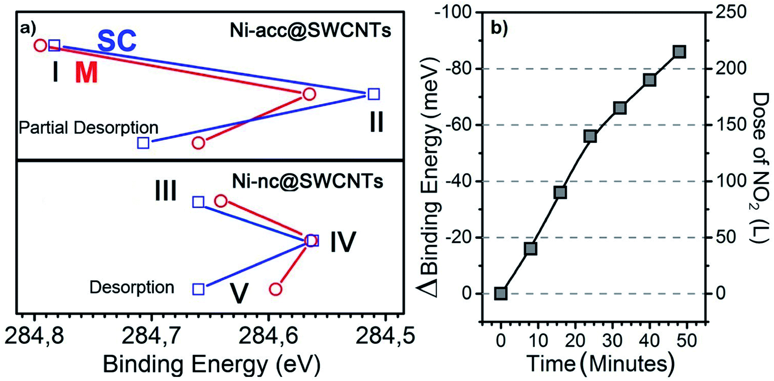
Further, selectivity and sensitivity were inspected by exposing the four types of materials to NO2 at different temperatures. The samples were exposed to NO2 and the influence of the gas dosage level, the filler states and temperature effects were tested in situ. To probe the relative interactions between SWCNTs and NO2 we carried out experiments in different representative stages for both metallic and semiconducting species as listed in Table 1. Stage I refers to the Ni-acc filled SWCNTs cooled to 100 K. This cooling allows for better resolution during the photoemission measurements. In stage II those samples were exposed to 80 L of NO2 (1 L ≈ 1.33 × 10⁻⁶ mbar s). The samples where then heated progressively to remove any remaining adsorbed species up to 500 °C, when the transformation to nanoclusters occurs in situ. Stage III then corresponds to the nanotubes filled with Ni clusters, which were first measured without exposure to NO2. In stage IV they were exposed to 80 L of NO2. Finally, the cluster filled tubes were observed until they reached room temperature without heating the sample in order to test the recovery efficiency under this condition (stage V). An approximation to the binding energy values of the C 1s core level has previously been reported for similarly filled nanotubes but in lab-based experiments.29,34,39,40 However, resolving these values at higher resolution can help in unraveling the type of adsorption mechanism occurring.24,41 The C 1s starting signals for metallic SWCNTs are slightly downshifted compared to the line of their semiconducting counterparts, and this can be associated with two effects: the possibility of different core hole screening in metallicity selected SWCNTs and different chemical potentials in bulk SWCNTs. However, the presence of the filler opens up a new scenario. Core hole effects are not visibly affected by metallicity; therefore the different core level binding energies here are mainly related to the chemical potentials. In Fig. 3a we can see how the C 1s binding energy shifts in the five mentioned stages. The values seen for molecule-filled semiconducting SWCNTs (∼284.77 eV) and the metallic SWCNTs (∼284.79 eV) are in very good agreement regarding their relative positions in comparison to those reported for clean metallicity sorted tubes also measured at low temperatures.28,29,40 In stage II, exposing the materials to NO2 produces for both – metallic and semiconducting tubes – a downshift of 230 and 260 meV in the C 1s position respectively. This can be attributed to charge transfer induced by the adsorption of NO2 acting as acceptor molecules.42,43 Here, the samples were left to recover without inducing changes externally. The desorption of the NO2 molecules and the recovery of the system can eventually bring C 1s to the original position. We continued however with our experiments with an intermediate high temperature heating step at 400 °C to accelerate the desorption procedure (which is otherwise very slow for the experimental facilities) and made sure that the remaining NO2 molecules were removed because we needed an adsorbent-free material for the subsequent transformation, which was performed in situ.39 Subsequently, as explained before, a 500 °C heat treatment was applied to transform the Ni-acc molecules into nanoclusters.33 This temperature range was maintained in order to obtain the highest possible filling ratio.34 Following the previous scheme, the nanocluster filled tubes were cooled to 100 K. The corresponding measurements are pictured with stage III as the starting point in the lower panel of Fig. 3a. Note that there is a slight difference between the position of C 1s corresponding to the materials with metallic and semiconducting hosts, which hints at a mildly different reactivity. However, when they are exposed to 80 L of NO2 in stage IV, the core level signal for both is very close. This does not mean that they go through the same reaction pathway but that they have a similar reactivity ratio when exposed to this type of gas. Taking into account I and III as initial stages, after NO2 exposure, in stages II and IV, in the case of the semiconducting hosts (blue lines), the differences in the binding energy of the C 1s line in the top panel compared to the bottom panel in Fig. 3a hint that the nanotubes filled with Ni-acc are more reactive compared to the systems filled with Ni-nc or that a physisorption process must be occurring. In such a case the shift is attributed to charge transfer between the tubes and the filler. On the other hand, when observing the recovery of the system while reaching ambient temperature in stage V in relation to III, the position of the C 1s line for the Ni-nc@SC-SWCNTs recovers almost completely compared to that for their counterparts, the metallic host tubes. Although both of these systems are able to reach a better recovery than the molecule-filled tubes, a preliminary conclusion would be that the first one (Ni-nc@M-SWCNTs) is more prone to chemisorption during exposure, while NO2 is mainly physisorbed to the Ni-nc@SC-SWCNTs. The picture is still incomplete and other parameters have to be taken into consideration. Previous studies on pristine SWCNTs have suggested the chemisorption of molecular species as induced reactions (including oxidation of the tubes by the NO2 molecules), are in turn assisted by the presence of reactive defects.18,41 But one of the complex problems to solve for sensors is how to reach full recovery at room temperature. For this, time resolved experiments on the Ni-nc@SC-SWCNTs were carried out with particular attention to the C 1s line and the valence band during the exposure to NO2 at room temperature. This differs from stages II and IV, which were carried out at 100 K. The experiments were performed with an increasing dose of NO2 over 50 minutes. As seen in Fig. 3b, the C 1s spectra corresponding to Ni-nc@SC-SWCNTs have a constant binding energy shift with increasing exposure to NO2. This is consistent with the shifts throughout the previously discussed stages but it is now necessary to understand the shape of the spectra. Further, Fig. 4 shows the deconvolution of the high resolution C 1s signals recorded for the semiconducting (left) and metallic (right) host species with a 525 eV excitation energy. The main sharp component around 284.5 eV in all the spectra corresponds to the main carbon peak.29,44,45 Additionally, a smaller component at slightly higher energy values (gray shaded area) is seen in Fig. 4a–d. This arises from the C atoms associated with the Ni-acc molecules. Note that this component has lower binding energy for the semiconducting and the metallic hosts filled with nanoclusters. It is also present in the bottom spectra (Fig. 4e and f) with much lower intensity, where it can be associated with Ni bonded to C, which in turn significantly decreases in the two cases where metallic clusters are formed.39 Furthermore, two types of carbon–oxygen bonds can be identified. The first one is attributed to atomic oxygen extracting a carbon atom and creating a defect in the lattice, leading to the formation of a ketene group, which applies to the hybrids before exposure to the NO2.24,41 The signal at 288.5 eV corresponds to the carboxylate group (O–C![[double bond, length as m-dash]](https://www.rsc.org/images/entities/char_e001.gif) O), which can be directly attributed to the Ni acetylacetonate filling. Upon conversion of the molecules into nanoclusters of Ni for both semiconducting and metallic hosts (Fig. 4e and f), the carboxylate group is not observable anymore.24,41 We can see here additionally, that the ketene and carboxylate signals are more pronounced for semiconducting hosts during the mid-range molecular exposure. This suggests that the presence of the molecules of Ni-acc inside the tubes allows for a higher interaction with the external surrounding gas. Note that the intensity variations and shift are more pronounced in the semiconducting hosts, indicating higher sensitivity.
O), which can be directly attributed to the Ni acetylacetonate filling. Upon conversion of the molecules into nanoclusters of Ni for both semiconducting and metallic hosts (Fig. 4e and f), the carboxylate group is not observable anymore.24,41 We can see here additionally, that the ketene and carboxylate signals are more pronounced for semiconducting hosts during the mid-range molecular exposure. This suggests that the presence of the molecules of Ni-acc inside the tubes allows for a higher interaction with the external surrounding gas. Note that the intensity variations and shift are more pronounced in the semiconducting hosts, indicating higher sensitivity.
 | ||
| Fig. 3 (a) Shift of the main peak of the C 1s core level signal in XPS of the semiconducting (blue) vs. metallic (red) hosts with different fillings at the stages listed in Table 1. (b) C 1s shift resulting from a time resolved experiment by exposing the Ni-nc@SC-SWCNTs to NO2. | ||
 | ||
| Fig. 4 C 1s core level spectra of Ni-acc@SC-SWCNTs (a) and Ni-acac@M-SWCNTs (b). The spectra correspondingly below (c and d) were recorded after exposure to 80 L of NO2. The bottom spectra correspond to Ni-nc@SC-SWCNTs (e) and Ni-nc@M-SWCNTs (f) exposed to 80 L of NO2. Molecular models are shown as the inset of each plot. | ||
To gain further insight, the valence band photoemission (VB-PES) response was recorded in UPS to obtain the integrated density of states as a function of the NO2 dosage concentration. VB-PES has previously been used on metallicity mixed SWNTs as a function of measurement cycles at increasing flashing temperatures.19 In contrast, we have performed measurements at ambient temperature pursuing the recovery of the systems under such conditions to corroborate the results discussed so far. Fig. 5a and b show the valence band recorded at three decisive stages, namely the cluster filled tubes without gas exposure, the spectra recorded at the maximum dosage and the recovery. Fig. 5c and d summarize the time resolved measurements at ambient temperature on the cluster filled tubes in two parts: during increasing exposure to NO2 and during recovery, both at room temperature. The plotted dots represent the variation of the total area of the valence band vs. the elapsed time of exposure and recovery (from Fig. 5a and b). Each dot corresponds to one measurement of the area of the valence band and it is calculated from: (As − Ao)/As × 100 where As is the area of the valence band during a single sweep and Ao is the area of the initial sweep before dosing up to 300 L of NO2 over a total time of ∼80 min. The line shading in Fig. 5c indicates the period of acquisition of the time resolved C 1s measurements.
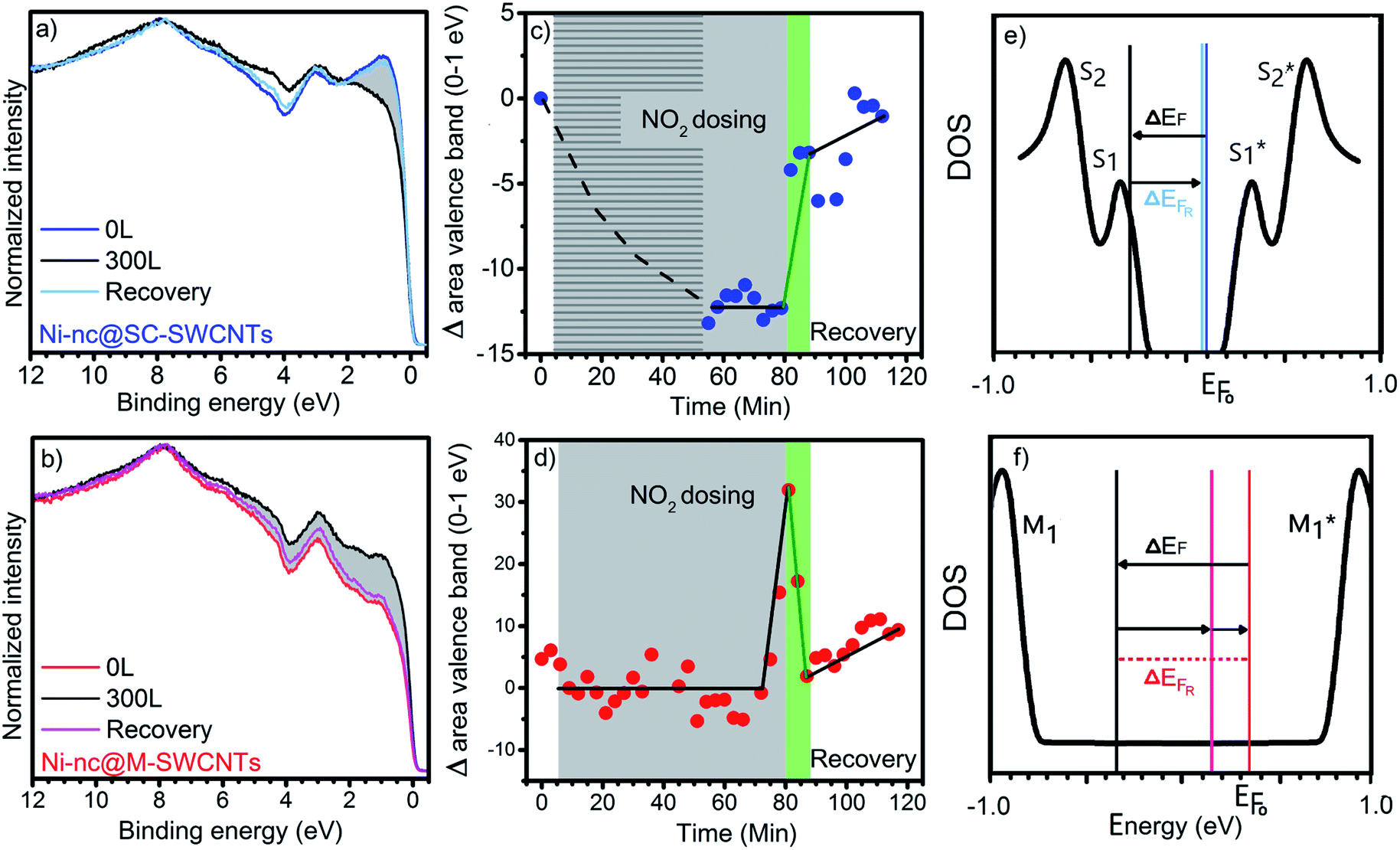 | ||
| Fig. 5 Valence band photoemission spectra of the Ni-nc@SC-SWCNTs (a) and Ni-nc@M-SWCNTs (b) showing the measurements before exposure to NO2, the spectrum at a maximum dosage of 300 L (black curves) and measurements after recovery (after final desorption of NO2). Integrated area of the valence band response close to the Fermi level (0–1 eV) as a function of the dosing and recovery time for the Ni-nc@SC-SWCNTs (c) and Ni-nc@M-SWCNTs (d). The gray shaded area corresponds to 80 min of continuous exposure to NO2 up to 300 L. This is followed by a 30 min recovery. The light green area indicates that most of the recovery already happened in the first 3 min. For the Ni-nc@SC-SWCNTs the overlapping shaded dosing area shows the time used to monitor the C 1s core level shift depicted in Fig. 3b. The right panels show sketches of the shifts in the VB in the density of states for both Ni-nc@SC-SWCNTs (e) and Ni-nc@M-SWCNTs (f). | ||
The VB-PES response in the Ni nanocluster filled SWCNT hybrids close to the Fermi level is governed by a superposition of the response of the SWCNTs and the Ni 4s band. On the other hand, we have seen so far that exposing these hybrid materials to NO2 yields a p-type doping of the SWCNTs which is reflected in a downshift of the C 1s binding energy. This hints that the chemical potential in the new hybrids is shifted towards the conduction band of the pristine and sorted SWCNTs. In the case of Ni-nc@SC-SWCNTs the chemical potential is pinned inside their energy gap 29 meV shifted to the onset of the conduction band at the S1* first van Hove singularity (vHs) as sketched in Fig. 5e. For the Ni-nc@M-SWCNTs, a shift of 19 meV indicates that the Fermi level remains still below the first vHs in the conduction band (M1*) and the constant density of states is filled during the gas exposure (Fig. 5f). In other words, the valence band response is related to a shift of the chemical potential into in the S1* in Ni-nc@SC-SWCNTs, which yields a lower DOS and a corresponding smaller signal in the VB-PES response and it is also direct and linear with the NO2 dosage. In the case of Ni-nc@M-SWCNTs the chemical potential shifts towards M1* and here the dosage influence is more complex as there is a constant DOS at the Fermi level between the M1 and M1* vHs to be depleted upon NO2 exposure before the first M1* vHs is reached. This means there is a strong time delay showing no effect with weakly chemisorbed NO2 beside a relative Fermi level shift in the first dosing steps. Only after the time dependent chemical reaction yielding NO2 decomposition products after 80 L dosage, an increase in the DOS is observed. After saturation dosage in both systems a fast recovery is observed within 3 minutes but the stronger chemisorption in the Ni-nc@M-SWCNTs does not allow a full recovery. This points out, that for sensing purposes the Ni-nc@S-SWCNTs are the better choice as they allow a fast recovery and detection which shows a linear response to NO2 dosage. Besides, they have a fast and even complete recovery at room temperature.
4 Conclusions
This work represents an important step towards understanding the ability of SWCNTs to behave as highly gas sensitive objects capable of recovering at ambient temperature. Metallicity sorted SWCNTs filled with metal nanoclusters have allowed us to define a pathway to achieve a reversible room temperature sensor for NO2. We find that the electronic structure in the vicinity of the Fermi level, which is in turn strongly related to the electron transport properties, is reversibly influenced by the NO2 adsorption mechanism. In other words, the changes in the Fermi level are directly related to the changes in the electronic properties while sensing. In situ PES experiments have revealed a remarkable result of sensitivity and recovery at ambient temperature. Regarding the selectivity criterion, the materials used in our experiments are an example of how to specifically tailor the selectivity towards NO2 in a reusable sensor. Inspired by this work, other reactive and poisonous gas species can be monitored by sensing targets with controlled and increased sensitivity and selectivity at room temperature.Conflicts of interest
There are no conflicts to declare.Acknowledgements
This work was supported by Austrian Science Fund through Project FWF P27769-N20. PA acknowledges the contribution of COST Action CA15107 (MultiComp). KY acknowledges support by JST CREST through Grant Number JPMJCR17I5, Japan. AG would like to acknowledge the NATO for project G5140.References
- A. Jorio, M. Dresselhaus and G. Dresselhaus, Carbon Nanotubes: Advanced Topics in the Synthesis, Structure, Properties and Applications, Springer-Verlag, Heidelberg, 2008 Search PubMed.
- R. H. Baughman, A. A. Zakhidov and W. A. De Heer, Science, 2002, 297, 787–792 CrossRef CAS PubMed.
- M. F. De Volder, S. H. Tawfick, R. H. Baughman and A. J. Hart, Science, 2013, 339, 535–539 CrossRef CAS PubMed.
- C. Li, E. T. Thostenson and T.-W. Chou, Compos. Sci. Technol., 2008, 68, 1227–1249 CrossRef CAS.
- J. Huang, A. L. Ng, Y. Piao, C.-F. Chen, A. A. Green, C.-F. Sun, M. C. Hersam, C. S. Lee and Y. Wang, J. Am. Chem. Soc., 2013, 135, 2306–2312 CrossRef CAS PubMed.
- D. R. Kauffman and A. Star, Angew. Chem., Int. Ed., 2008, 47, 6550–6570 CrossRef CAS PubMed.
- A. Goldoni, L. Petaccia, S. Lizzit and R. Larciprete, J. Phys.: Condens. Matter, 2010, 22, 013001 CrossRef CAS PubMed.
- D. Kumar, P. Chaturvedi, P. Saho, P. Jha, A. Chouksey, M. Lal, J. Rawat, R. Tandon and P. Chaudhury, Sens. Actuators, B, 2017, 240, 1134–1140 CrossRef CAS.
- J. Zhao, A. Buldum, J. Han and J. P. Lu, Nanotechnology, 2002, 13, 195 CrossRef CAS.
- S. Santucci, S. Picozzi, F. Di Gregorio, L. Lozzi, C. Cantalini, L. Valentini, J. Kenny and B. Delley, J. Chem. Phys., 2003, 119, 10904–10910 CrossRef CAS.
- G. Gruner, Anal. Bioanal. Chem., 2006, 384, 322–335 CrossRef CAS PubMed.
- S. Boussaad, B. A. Diner and J. Fan, J. Am. Chem. Soc., 2008, 130, 3780–3787 CrossRef CAS PubMed.
- H. Chang, J. D. Lee, S. M. Lee and Y. H. Lee, Appl. Phys. Lett., 2001, 79, 3863–3865 CrossRef CAS.
- N. Peng, Q. Zhang, C. L. Chow, O. K. Tan and N. Marzari, Nano Lett., 2009, 9, 1626–1630 CrossRef CAS PubMed.
- J. Li, Y. Lu, Q. Ye, M. Cinke, J. Han and M. Meyyappan, Nano Lett., 2003, 3, 929–933 CrossRef CAS.
- H.-F. Kuo, D.-H. Lien, W.-K. Hsu, N.-H. Tai and S.-C. Chang, J. Mater. Chem., 2007, 17, 3581–3584 RSC.
- D. Mowbray, C. Morgan and K. S. Thygesen, Phys. Rev. B: Condens. Matter Mater. Phys., 2009, 79, 195431 CrossRef.
- J. M. García-Lastra, D. Mowbray, K. S. Thygesen, A. Rubio and K. W. Jacobsen, Phys. Rev. B: Condens. Matter Mater. Phys., 2010, 81, 245429 CrossRef.
- A. Goldoni, R. Larciprete, L. Petaccia and S. Lizzit, J. Am. Chem. Soc., 2003, 125, 11329–11333 CrossRef CAS PubMed.
- J. A. Robinson, E. S. Snow, S. C. Badescu, T. L. Reinecke and F. K. Perkins, Nano Lett., 2006, 6, 1747–1751 CrossRef CAS PubMed.
- L. Valentini, F. Mercuri, I. Armentano, C. Cantalini, S. Picozzi, L. Lozzi, S. Santucci, A. Sgamellotti and J. Kenny, Chem. Phys. Lett., 2004, 387, 356–361 CrossRef CAS.
- J. Kim, S.-W. Choi, J.-H. Lee, Y. Chung and Y. T. Byun, Sens. Actuators, B, 2016, 228, 688–692 CrossRef CAS.
- K. Yanagi, H. Udoguchi, S. Sagitani, Y. Oshima, T. Takenobu, H. Kataura, T. Ishida, K. Matsuda and Y. Maniwa, ACS Nano, 2010, 4, 4027–4032 CrossRef CAS PubMed.
- G. Ruiz-Soria, A. Perez Paz, M. Sauer, D. John Mowbray, P. Lacovig, M. Dalmiglio, S. Lizzit, K. Yanagi, A. Rubio, A. Goldoni, P. Ayala and T. Pichler, ACS Nano, 2014, 8, 1375–1383 CrossRef CAS PubMed.
- H. Ulbricht, R. Zacharia, N. Cindir and T. Hertel, Carbon, 2006, 44, 2931–2942 CrossRef CAS.
- M. D. Ellison, M. J. Crotty, D. Koh, R. L. Spray and K. E. Tate, J. Phys. Chem. B, 2004, 108, 7938–7943 CrossRef CAS.
- K. Yanagi, R. Moriya, N. T. Cuong, M. Otani and S. Okada, Phys. Rev. Lett., 2013, 110, 086801 CrossRef PubMed.
- P. Ayala, H. Shiozawa, K. De Blauwe, Y. Miyata, R. Follath, H. Kataura and T. Pichler, J. Mater. Sci., 2010, 45, 5318–5322 CrossRef CAS.
- P. Ayala, Y. Miyata, K. De Blauwe, H. Shiozawa, Y. Feng, K. Yanagi, C. Kramberger, S. Silva, R. Follath, H. Kataura and T. Pichler, Phys. Rev. B: Condens. Matter Mater. Phys., 2009, 80, 205427 CrossRef.
- B. S. Hammes and C. J. Carrano, Inorg. Chem., 1999, 38, 3562–3568 CrossRef CAS PubMed.
- M. Utriainen, M. Kröger-Laukkanen, L.-S. Johansson and L. Niinistö, Appl. Surf. Sci., 2000, 157, 151–158 CrossRef CAS.
- O. Domanov, E. Weschke, T. Saito, H. Peterlik, T. Pichler, M. Eisterer and H. Shiozawa, Nanoscale, 2019, 11, 10615–10621 RSC.
- H. Shiozawa, A. Briones-Leon, O. Domanov, G. Zechner, Y. Sato, K. Suenaga, T. Saito, M. Eisterer, E. Weschke, W. Lang, H. Peterlik and T. Pichler, Sci. Rep., 2015, 5, 15033 CrossRef CAS PubMed.
- M. Sauer, A. Briones-Leon, T. Saito, K. Yanagi, K. Schulte, T. Pichler and H. Shiozawa, Phys. Status Solidi B, 2015, 252, 2546–2550 CrossRef CAS.
- G. Nemeth, D. Datz, A. Pekker, T. Saito, O. Domanov, H. Shiozawa, S. Lenk, B. Pecz, P. Koppa and K. Kamaras, RSC Adv., 2019, 9, 34120–34124 RSC.
- K. Kim and N. Winograd, Surf. Sci., 1974, 43, 625–643 CrossRef CAS.
- B. Löchel and H.-H. Strehblow, J. Electrochem. Soc., 1984, 131, 713–723 CrossRef.
- H. Nesbitt, D. Legrand and G. Bancroft, Phys. Chem. Miner., 2000, 27, 357–366 CrossRef CAS.
- M. Sauer, H. Shiozawa, P. Ayala, G. Ruiz-Soria, H. Kataura, K. Yanagi, S. Krause and T. Pichler, Phys. Status Solidi B, 2012, 249, 2408–2411 CrossRef CAS.
- P. Ayala, H. Shiozawa, K. De Blauwe, Y. Miyata, R. Follath, H. Kataura and T. Pichler, J. Mater. Sci., 2010, 45, 5318–5322 CrossRef CAS.
- D. J. Mowbray, A. P. Paz, G. Ruiz-Soria, M. Sauer, P. Lacovig, M. Dalmiglio, S. Lizzit, K. Yanagi, A. Goldoni, T. Pichler, P. Ayala and A. Rubio, J. Phys. Chem. C, 2016, 120, 18316–18322 CrossRef CAS.
- J. Kong, N. R. Franklin, C. Zhou, M. G. Chapline, S. Peng, K. Cho and H. Dai, Science, 2000, 287, 622–625 CrossRef CAS PubMed.
- R. Larciprete, S. Ulstrup, P. Lacovig, M. Dalmiglio, M. Bianchi, F. Mazzola, L. Hornekær, F. Orlando, A. Baraldi, P. Hofmann and S. Lizzit, ACS Nano, 2012, 6, 9551–9558 CrossRef CAS.
- T. Susi, D. J. Mowbray, M. P. Ljungberg and P. Ayala, Phys. Rev. B: Condens. Matter Mater. Phys., 2015, 91, 081401 CrossRef.
- K. De Blauwe, D. J. Mowbray, Y. Miyata, P. Ayala, H. Shiozawa, A. Rubio, P. Hoffmann, H. Kataura and T. Pichler, Phys. Rev. B: Condens. Matter Mater. Phys., 2010, 82, 125444 CrossRef.
Footnote |
| † Electronic supplementary information (ESI) available. See DOI: 10.1039/d0ta02749a |
| This journal is © The Royal Society of Chemistry 2020 |