
 Open Access Article
 This Open Access Article is licensed under a Creative Commons Attribution-Non Commercial 3.0 Unported Licence
Prospects for defect engineering in Cu2ZnSnS4 solar absorber films†
Katharina
Rudisch
 ,
Alexandra
Davydova
,
Lars
Riekehr
,
Joakim
Adolfsson
,
Luciano
Quaglia Casal
,
Charlotte
Platzer-Björkman
and
Jonathan
Scragg
*
,
Alexandra
Davydova
,
Lars
Riekehr
,
Joakim
Adolfsson
,
Luciano
Quaglia Casal
,
Charlotte
Platzer-Björkman
and
Jonathan
Scragg
*
Solar Cell Technology, Ångström Solar Center, Uppsala University, Box 534, SE-751 21 Uppsala, Sweden. E-mail: jonathan.scragg@angstrom.uu.se
First published on 29th April 2020
Abstract
Complex compound semiconductors, such as the emerging solar cell material Cu2ZnSn(S,Se)4 (CZTS), present major experimental challenges in terms of understanding and controlling growth processes and defect formation. This study aims to shed light upon the complicated interplay of the synthesis conditions and CZTS thin film properties. Composition-spread thin films are fabricated in different atmospheric conditions during the annealing step. The span of the single-phase region is identified by a phase analysis combining XRD and Raman mapping. The phase characterisation is strengthened by STEM-EDX analysis. Our results show that the stability of the CZTS phase is strongly affected by the process conditions which is observed as a shift in the secondary phase boundaries and different levels of maximum cation ordering achieved in the different samples. With regard to the photoluminescence intensity, all investigated samples show the same trends: regions with Cu3SnS4 secondary phase show the lowest intensity, while the presence of SnSx secondary phases greatly enhances the photoluminescence intensity. The single-phase region features an overall low photoluminescence intensity without a remarkable composition dependence and we propose the presence of deep defects in absence of secondary phases that limit the radiative recombination. We discuss implications for future efforts in defect engineering toward improving the efficiency of CZTS thin film devices.
1 Introduction
Advanced technologies for clean energy, health and sustainable living will be enabled by new and improved materials. Complex compound semiconductors containing at least three elements in their structures are a material class with special importance, since they have critical renewable energy conversion applications. Modern materials screening methods are continuing to identify new candidate compound semiconductors, many from unexplored landscapes of the periodic table including inorganic pnictides, chalcogenides and halides.1–6 However, for such complex materials, providing confident judgement on practical potential and homing in on optimal growth conditions are major challenges.An interesting case in point is the “emerging” semiconductor Cu2ZnSn(S,Se)4 (CZTS) which is an earth-abundant, low-toxicity alternative to the thin film solar cell material Cu(In,Ga)Se2. CZTS, or “kesterite”, has been in intensive research for several decades, and while it remains the frontrunner among all-inorganic earth abundant, direct band gap materials,7 solar cell conversion efficiencies have stagnated at a level far below that of CIGS and other competing solar cell technologies (including hybrid and organic).8 Despite this, the high stability of inorganic materials as well as the absence of rare or toxic elements are crucial arguments for continued research into CZTS.
The fundamental bottleneck in the case of CZTS seems to be avoidance of deep defects (or deep potential fluctuations caused by abundant defects) that pin the open circuit voltages in CZTS solar cells well below the upper limit of the material band gap (1–1.5 eV depending on S/Se ratio).9,10 Several candidate defects are proposed, including S vacancies stabilised by Sn(II), SnZn point defects and Cu–Zn disorder11,12 Therefore, many reports point out the need for strategies to suppress detrimental defects in the material that are responsible for bulk recombination.13,14 Disregarding their specific nature, these defects must form during material growth – as a polycrystalline thin film – typically at temperatures in the 400−600 °C range, and their populations will be influenced by both kinetic and thermodynamic factors. These factors are affected strongly by non-stoichiometry (it is well-known that CZTS can adopt an appreciable range of off-stoichiometric compositions, due to the formation of numerous neutral defect complexes15,16). In terms of kinetics, mass transport by diffusion during crystallisation and annealing will determine the rate of most defect formation or elimination processes. Diffusive transport can be assisted by presence of certain defect complexes17,18 at different stoichiometries, secondary phases19 and grain boundaries;20 the same factors strongly influence the rate of grain growth and the final morphology of the polycrystalline thin film. All these processes have a strong temperature dependence. In terms of thermodynamics, formation energies of defects are modified by chemical potentials of the constituent elements – again linked to stoichiometry.21
According to this framework, changing either the CZTS stoichiometry or growth conditions (e.g. temperature and time) can affect the defect formation energies, the reaction rates and the reaction progress of all growth processes (i.e. how near to thermodynamic equilibrium the system reaches during the allotted process time). These effects may provide a route for control of detrimental defects, i.e. to conduct defect engineering. However, the complicated interplays described mean that compositional and process variations cannot be studied in isolation if we wish to obtain a clear understanding of how defect formation in CZTS – or similarly complex materials – can be controlled.
Due to the central role of stoichiometry in growth and defect formation processes, a powerful way to study them is to use composition-spread (CS) samples, in which thin film samples are prepared with gradients in composition and characterised by spatially-resolved methods, so as to derive composition-dependent properties. By linking observed behaviours with composition trends, it is possible to glimpse some of the underlying mechanisms. Besides the study of defects, such studies give valuable insight into the formation and influences of secondary phases as well as phase boundary equilibria (see e.g.ref. 22).
The method of studying CS films involves several challenges. First, the integral film composition at a certain point should not be mistaken for the composition of the CZTS phase. This is because secondary phases coexist in the film.23 Therefore, it is important to carefully identify regions with secondary phases and the single-phase region (SPR) on a CS sample in order to be able to assess the composition of the CZTS phase. Davydova et al.24 propose a chemical model for the SPR that can be used to interpret the composition of the CZTS phase for a CS sample. A second challenge is the narrow composition range of the SPR25 for CZTS. Due to the volatility of Sn–S phases26 the SPR is typically reduced to a small composition window.27 When single-phase regions can be accurately determined in CS samples, it is possible to distinguish influences from intrinsic CZTS properties from those of secondary phases.
In this work, we study the interrelations of growth process conditions and composition in exemplary CS films of CZTS to illustrate the power and utility of the CS approach. We perform a careful secondary phase identification based on mapping of multiwavelength Raman spectroscopy and X-ray diffraction (XRD) line scans. Scanning transmission electron microscopy (STEM) combined with energy dispersive X-ray (EDX) spectroscopy at several positions across the investigated samples confirms the phase assignments. We characterise intrinsic qualities of the CZTS phase using resonant Raman spectroscopy and photoluminescence. The results reveal an intimate connection between the quality of the CZTS phase itself and the presence of SnSx secondary phases, a connection which is preserved for large variations in growth conditions. This connection, obvious in CS samples, would have been very difficult to make using traditional methods. It also leads to some concerning conclusions on the prospects for defect engineering in CZTS.
2 Experimental methods
Composition-spread (CS) CZTS films with a cation composition gradient were prepared in a two-step process. First, Cu–Zn–Sn–S precursor films were deposited by co-sputtering on 70 × 70 mm2 Mo-covered soda-lime glass substrates. The sputtering process was performed in a Lesker CMS-18 sputter system with compound targets CuS, ZnS and SnS installed in an equilateral triangular arrangement such that they have equal distance to each other and equal distance to the substrate holder. During the deposition, the substrate holder was heated to 250 °C and the sputtering pressure was held at 5 mTorr with a constant Ar-flow of 50 sccm. The CuS and SnS targets were DC sputtered with 71 W and 24 W, respectively. The ZnS target was rf-sputtered with 165 W. The sputter time was 1600 s yielding films with a thickness of about 400 nm. The substrate holder was not rotated during depositions leading to the gradients of cation composition across the sample area. The anion composition is determined by the cation composition and is roughly constant. The precursor composition at each corner was measured by XRF, allowing a suitable 50 × 50 mm2 region to be cut out for further processing. Crystallisation of the sputtered precursors was initiated by an annealing process in a tube furnace. The precursors were placed in a pyrolytic carbon-coated graphite box, which was then inserted into the hot zone of the tube furnace for rapid heating. The annealing was performed at 550 °C and at constant argon atmosphere of 35.3 kPa. After the annealing time, the graphite box was removed from the hot zone and cooled naturally to below 200 °C within 3 min.In this study, initially identical precursors were annealed in three different processes designed to cause large perturbations to growth conditions. For the first sample (A), 40 mg of elemental sulphur pellets was added to the graphite box to provide S vapour during the anneal step according to the reaction
| S(s) → S8(g), S7(g), …S2(g). | (1) |
The annealing period was 13 minutes; this corresponds to our baseline annealing process used to achieve CZTS solar cells with 9.7% efficiency.28 The next sample (B) was annealed in the same way but for only two minutes. For samples A and B, the chemical potential of S (defined by its partial pressure29) will evolve along the same curve, with partial pressure dropping with time due to leakage from the box. The shorter time for B reduces the window for grain growth and the formation of equilibrium phases and defects, but also allows retention of a higher S pressure in the anneal zone.30 For sample C, the graphite box was preconditioned with SnCl2 and elemental sulphur to yield SnS2 in the box as described in ref. 24. Then the precursor of sample C and 30 mg of Cu(II)S powder (purity of 99.99% trace metal basis) as sulphur source were added in the box and the sample was annealed for 13 minutes. The intention here is to maximise the partial pressures of gaseous species S and SnS via the reactions
| 4CuS(s) → 2Cu2S(s) + S2(g) | (2) |
| 2SnS2(s) → 2SnS(s/g) + S2(g). | (3) |
It is noted that the S2 partial pressure arising from CuS as denoted in Reaction (2) is higher than that arising from elemental S as denoted in Reaction (1).31 The annealing conditions for samples A–C are illustrated in Fig. 1.
 | ||
| Fig. 1 Sample overview illustrating the different processing conditions during the annealing step in terms of annealing time and atmosphere. The annealing temperature is 550 °C. | ||
After the anneal, a separate low temperature treatment was performed on each sample to maximize the cation order in the CZTS films according to ref. 32. To achieve this, the crystalline CS CZTS films were again placed in a coated graphite box and heated in the hot zone of a tube furnace to 273 °C. Then the hot zone was cooled to 80 °C at a rate of 0.1 K min−1.
The cation composition across the CS samples was mapped in a Leo Zeiss 1550 system by energy dispersive X-ray spectroscopy (EDX) with 20 keV accelerating voltage, analogously to ref. 24 (the same system was also used to capture scanning electron microscopy (SEM) images, with 10 keV accelerating voltage using the InLens detector). Composition data points were taken at 1.5–2 mm intervals across each sample. The measured Cu, Zn and Sn percentages were fitted with two-dimensional surface polynomials of 4th (3rd) order in both X and Y directions for Cu (Zn and Sn). In this way, the mapping coordinates for the subsequent analysis techniques could be freely chosen and did not need to correspond to the EDX mapping coordinates. Note that S content was not characterised due to peak overlap with Mo from the substrate.
Multiwavelength Raman spectroscopy was performed in a Renishaw inVia micro-Raman system with excitation wavelengths 325 nm, 532 nm and 785 nm. The system was calibrated with a Si-reference sample using the characteristic peak at 520 cm−1. Photoluminescence mapping was performed in the same system with the 532 nm excitation wavelength. The photoluminescence was evaluated within the energy range from 1.25–1.55 eV. This is the range where the photoluminescence maximum of CZTS is expected.
The different crystallographic phases were analysed by grazing-incidence X-ray diffraction (GIXRD) in a Philips MRD X'Pert diffractometer with K alpha radiation. For spatially resolved measurements, a slit was applied to the primary beam exit, narrowing the investigated region on the sample to a 2 mm wide (but elongated) area. Automated stage control was used for scanning along the y-coordinate of the sample holder to obtain information linescan across the full sample (this is depicted in a sketch in Fig. S9 in the ESI†).
For scanning transmission electron microscopy (STEM) analysis, site specific cross-section samples of the thin films were prepared with a focused ion beam and a scanning electron microscope (FIB-SEM, FEI Strata DB325). The extracted lamellae were then attached to a Ti lift out grid and thinned to electron transparency with a last polishing step using a 5 kV Ga-ion beam. Scanning transmission electron microscopy (STEM) analysis was performed with a probe corrected FEI Titan Themis operated at 200 kV and equipped with an X-FEG and a SuperX energy dispersive X-ray (EDX) spectroscopy system. The EDX spectral images were quantified with the software ESPRIT 1.9 developed by Bruker, using theoretical Cliff–Lorimer factors provided by ESPRIT (standardless quantification). For better visualization, the acquired elemental maps are plotted with Matlab.
3 Results
3.1 Secondary phases and single-phase regions
For this study, three CS CZTS films were fabricated with the same sputter process but with different annealing conditions as summarized in Fig. 1. From EDX mapping, the samples showed a wide composition range across the sample area, including the compositions that are expected to comprise the single-phase region (SPR) and areas with various secondary phases. The samples were first characterised by multiwavelength Raman mapping. This technique yields valuable information about the CZTS phase itself (see later), as well as the near-surface secondary phases ZnS and Cu3SnS4 (and in some cases Sn–S phases) using excitation wavelengths of 785 nm (for CZTS and Cu3SnS4 phase analysis) and 325 nm (for ZnS phase analysis).24 Here, we also show analysis of the phase boundary of CuS secondary phases with Raman spectroscopy. CuS has a characteristic Raman mode at 474 cm−1 which can be observed under excitation with 532 nm and 325 nm.33 The vibration modes used for characterisation together with the suited excitation wavelength are listed in Table 1.| Characteristic Raman mode | Excitation wavelength | |
|---|---|---|
| Cu2ZnSnS4 | 338 cm−1 | 785 nm |
| CuS | 475 cm−1 | 532 nm (325 nm) |
| ZnS | 697 cm−1 (2nd order mode) | 325 nm |
| Cu3SnS4 | 318 cm−1 | 785 nm |
As an example, Fig. 2(a) shows a Raman spectrum from the Cu-rich side of sample B under 532 nm excitation. The spectrum shows the typical Raman modes of CZTS in the range 250–400 cm−1. The peak at 475 cm−1 however indicates the existence of CuS. By recording such spectra at a grid of points across the CS samples, and integrating the intensity in the relevant region of each spectrum, maps of peak intensity can be generated. Based on the EDS composition fits, the peak intensity can be plotted on compositional, as opposed to spatial, axes. This is shown in Fig. 2(b). The intensity in the region of the CuS mode increases indeed towards the Cu-rich side of the CS sample. To identify the exact boundary of the secondary phase region for CuS the Raman spectra were analysed individually to determine the coordinates and then compositions for which CuS peaks vanished. The phase boundaries of ZnS and Cu3SnS4 were analysed analogously. Corresponding Raman intensity maps for the other phases and samples are found in the ESI (Fig. S1–S8†). Further information regarding analysis of the secondary phase boundaries of ZnS and Cu3SnS4 from Raman mapping can be found in the work by Davydova et al.24
 | ||
| Fig. 2 (a) Raman spectrum (532 nm excitation) with CZTS Raman modes in the range 250–400 cm−1. CuS mode visible at 475 cm−1. (b) Integrated intensity in the region of the CuS peak against the cation composition from EDX. The phase boundary for CuS is marked with a white dashed line. | ||
While CuS, ZnS and Cu3SnS4 are easily observed by Raman, SnSx secondary phases are often hidden at the back of the CZTS layer. Therefore, characterisation with surface sensitive Raman spectroscopy is difficult.24 Instead, grazing incidence X-ray diffraction (GIXRD) can be used to study the occurrence of SnSx secondary phases because the diffraction patterns show several distinct reflections.30
GIXRD scans were made for linear regions of the CS samples about 1–2 mm wide, perpendicular to the Cu/Sn composition axis; the boundaries of the SnSx related secondary phase region are expected to lie in this direction according to theoretical studies of the SPR25 and experimental analysis of the SPR of CS samples.24 A sketch illustrating the linescanning on a CS sample with GIXRD is shown in the ESI in Fig. S9.† To capture the required information with high quality, small angular ranges were scanned about the known positions of SnSx reflections (see Fig. 3(a) and 4).
 | ||
| Fig. 3 (a) XRD patterns in regions with SnS2 reflection at 15° for different positions parallel to the Cu/Sn = 2 line on sample B. y denotes the distance to the Cu/Sn = 2 line in mm. (b) Integrated intensity of the reflection at 15°. The dotted lines are guides to the eye for the interpolation to the phase boundary. | ||
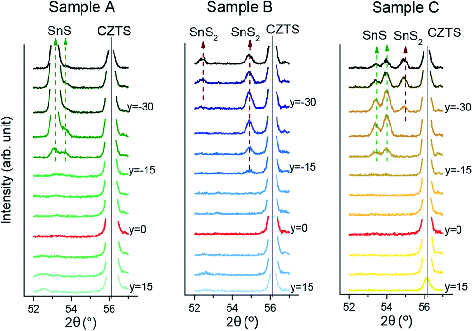 | ||
| Fig. 4 XRD patterns of samples A, B and C in a 2θ range with expected SnS and SnS2 reflections. y denotes the distance to the Cu/Sn = 2 line in mm. | ||
All three samples featured the same reflection at 15° in the Sn-rich region of the sample, which can be assigned to the SnS2 phase. Sample B also shows two more SnS2 peaks, at 52.5° and at 55° (Fig. 3). Samples A and C additionally show SnS peaks at 53.5° and 54°, but the peak ratios are very different, suggesting different texturing of the SnS phase.
The SnS2 reflection at 15° was strongest and therefore was used to mark the boundary of the CZTS SPR toward Sn-rich compositions. To define the position of the boundary, the intensity of the peak was integrated for each pattern and plotted against the perpendicular distance of the measurement from the Cu/Sn = 2 stoichiometric line (see Fig. 3(b)). This position is then translated into cation compositions for each sample. The final SnSx phase boundaries are depicted for all three CS samples in Fig. 5. Sample A and B have their SnSx phase boundaries at a similar, moderate Sn-rich composition with Cu/Sn ≈ 1.8. The boundary for sample C is further from the stoichiometric line, at a composition around Cu/Sn ≈ 1.6.
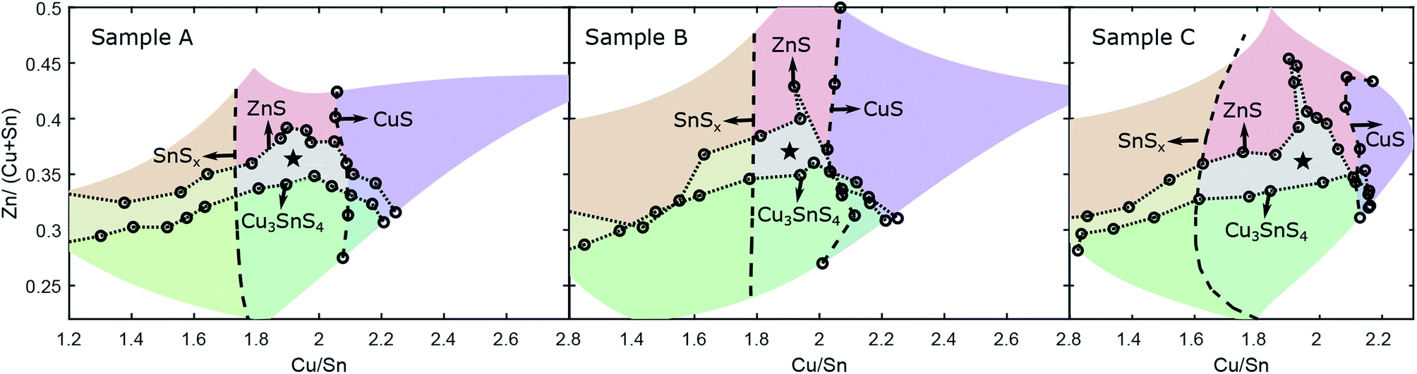 | ||
| Fig. 5 Phase boundaries from Raman and XRD measurements for samples A, B and C. The regions with secondary phases are shaded in different colours. The CZTS single-phase region is denoted with a star. | ||
Samples A and B featured a minor reflection at 52.5° on the Cu-rich side. This confirms the Raman-based identification of CuS in this region. Unfortunately the XRD peak intensity was too low to make a comparative estimate for the CuS phase boundary.
The differences in Sn–S secondary phase formation and boundary position provide a window onto the anneal conditions experienced by the three CS samples, which differ in the partial pressures of the gaseous components S and SnS experienced throughout their anneal processes. It would appear that sample B (2 min anneal with S vapour) had the greatest partial pressure of S at the point at which the sample was quenched, which shows in the complete oxidation of the excess Sn content to SnS2. Sample A, with the same conditions but a longer anneal time, experienced a lower partial pressure due to leakage of S vapour from the sample box. This resulted in decomposition of some SnS2 to SnS,30 without changing the position of the phase boundary. Sample C is a different case: the phase boundary itself is further from stoichiometry, which is the expected result of enhancing the SnS partial pressure, due to stabilisation of Sn-rich defect complexes in the CZTS phase (see Davydova et al.24). The different SnS and SnS2 peaks observed for samples A/B compared to C suggest different formation routes for these phases. Three formation routes are possible; (a) direct precipitation from the precursor, (b) decomposition of CZTS due to oversaturation with Sn or surface/back contact decomposition or (c) condensation from the anneal atmosphere. The last option seems less likely because SnS was never observed outside the Sn-rich region, whereas condensation could in principle occur at any point on the sample.
Combining the phase boundaries derived from Raman and XRD experiments gives a complete picture of the secondary phase distribution across the CS samples as well as defining the region where only the Cu2ZnSnS4 phase is present, i.e. the single-phase region (SPR). This is shown for all three samples in Fig. 5. The results are in good agreement with previous examples.24 The phase boundaries for Zn-rich and Zn-poor compositions are similar in each case, showing the notable extension of the SPR toward very Zn-rich compositions – Zn/(Cu + Sn) = 0.4–0.45 – in the vicinity of Cu/Sn = 2. At the same time, any Zn-deficiency results in immediate decomposition to (in this instance) CZTS + Cu3SnS4. In terms of the SnSx boundaries, the differences discussed above are clear. For Cu-rich compositions, the SPR barely crosses the Cu/Sn = 2 line, indicating that CuS is formed readily, although for sample C the SPR extends slightly further to Cu-rich compositions. The extended SPR in sample C indicates that the stability of CZTS is enhanced in the growth conditions chosen, resulting in greater tolerance to off-stoichiometry.
3.2 Morphology and phase distribution
To obtain additional confirmation of the assigned secondary phases as well as to observe the film morphology in different phase regions, the CS samples were further analysed by STEM and STEM-EDX measurements, extracting lamellae from several positions across the sample area. Fig. 6 shows six bright-field STEM images from selected points on sample A, indicating the respective phase regions based on XRD and Raman spectroscopy.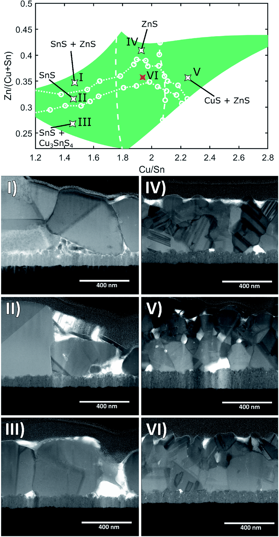 | ||
| Fig. 6 Outline of sample A with boundaries for secondary phase regions. Bright field STEM images of samples extracted from positions as indicated in the map. | ||
The STEM images of positions (I)–(III) show large, rounded CZTS grains expanding over the entire thickness of the film with few crystal defects (e.g. twins and stacking faults) visible. The common feature in these regions is the presence of SnSx phases alongside CZTS. This is in contrast to positions (IV)–(VI), which exhibit smaller grains with abundant crystal defects in the CZTS grains, most especially for position (IV), in the Zn-rich region. Similar results are observed for samples B and C (see ESI Fig. S13 and S14†). It is noted that the CZTS grain size in sample B for a similar composition is not substantially smaller than in A, despite the shorter annealing time.
STEM EDX maps at the same locations were used to identify phase segregations in the films. In the regions with identified secondary phases, corresponding inhomogeneities were found in EDX maps. Exemplary cases are shown in Fig. 7 and 8 and the rest are found in the ESI (Fig. S10–S12†). Notably, no chemical inhomogeneities were detected with EDX mapping for samples taken from the single-phase regions (see e.g.Fig. 7(c)). Fig. 7(a) shows sample A at position (V), where CuS and ZnS should occur. In agreement with the Raman analysis, CuS and ZnS grains are detected alongside the bulk Cu2ZnSnS4 phase. Both secondary phases tend to locate close to the film surface as reported by,34 but smaller grains are also found throughout the bulk of the film. For the other positions, the expected secondary phases were always detected (see ESI†), except for position (III), where the ternary phase Cu3SnS4 is the dominant signal detected with Raman spectroscopy, and SnSx in XRD. In the STEM-EDX maps for this phase region (see Fig. 7(b)), one can identify regions with high Sn content, suggesting Sn-related secondary phases, as well as small regions with high Cu content which seem to be CuS grains. The latter observation is unexpected based on the Cu-poor composition at this position (Cu/Sn ≈ 1.5) but may be explained by decomposition of the CZTS phase in contact with Mo (see e.g.ref. 35). More surprisingly, no inclusions of Cu3SnS4 are observed in this sample, despite the strong Raman signals. We propose that Cu3SnS4 does not form separate grains but rather appears as a solid solution with Cu2ZnSnS4 (i.e. Cu(3−x)ZnxSnS4), due to the high degree of structural similarity between disordered kesterite and Cu3SnS4.36 The Raman signal can be attributable simply to motifs of the Cu3SnS4 structure appearing within the solid solution at the nanoscale, strongly enhanced due to the resonant effect arising from the similarity of the Cu3SnS4 band gap to the excitation laser energy (1.6 eV (ref. 37) cf. 1.58 eV). Despite this interesting exception, the general conclusion is that the STEM-EDX measurements strongly support the XRD and Raman phase assignments as well as revealing clear differences in the growth of the CZTS film for different compositions and anneal conditions.
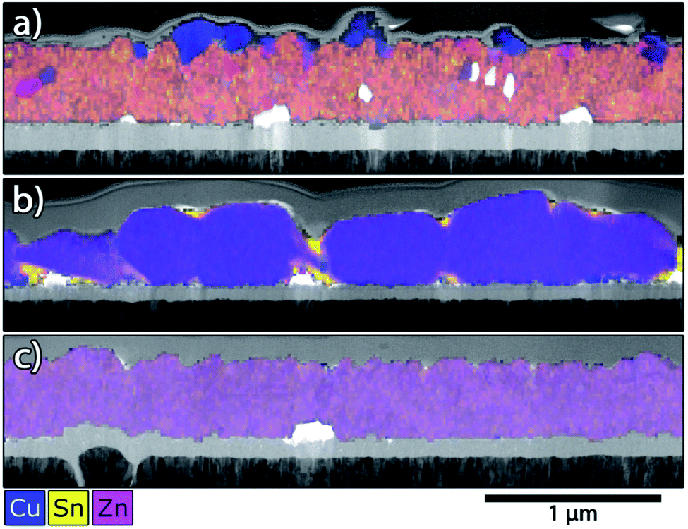 | ||
| Fig. 7 STEM and EDX images of sample A. Cu, Zn and Sn are marked by the colors blue, magenta and yellow, respectively. (a) Sample taken at position (V). (b) Sample taken at position (III). (c) Sample taken from the SPR at position (VI). | ||
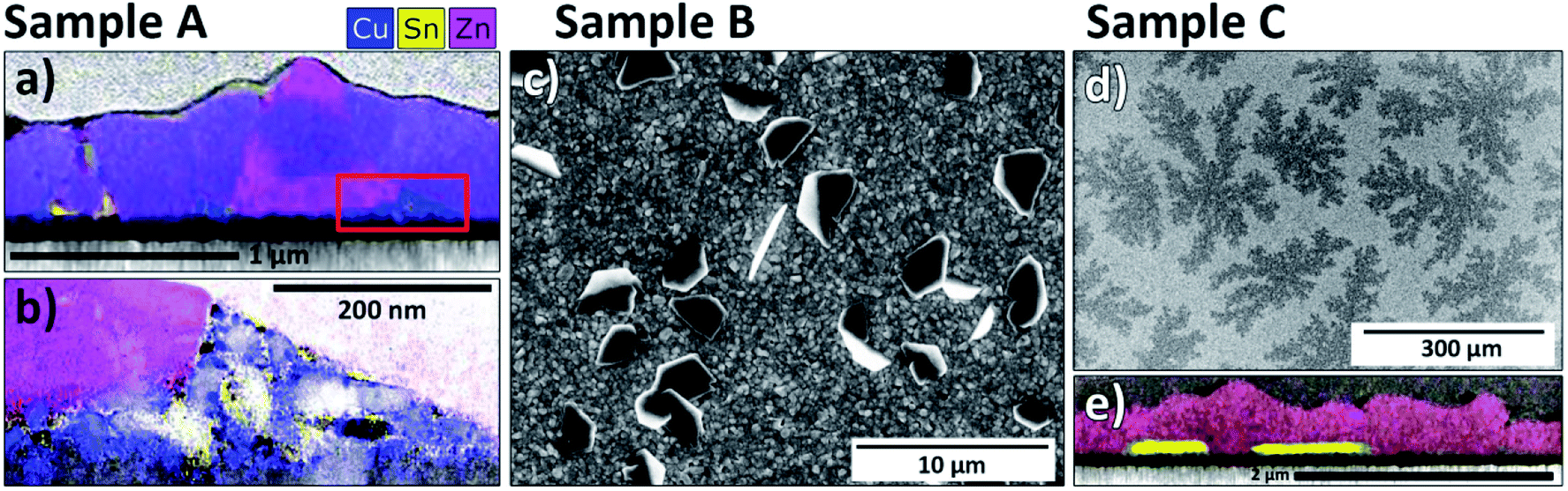 | ||
| Fig. 8 Observation of SnSx secondary phases in samples A, B and C. Sample A: STEM and EDX images, (a) with Cu (blue), Zn (pink) and Sn (yellow) and (b) close-up image of area marked with red rectangle. Sample B: (c) top view SEM with SnSx flakes visible on surface. Sample C: (d) top view SEM with dendrite structures. (e) STEM and EDX image with Sn (yellow) and Zn (magenta). | ||
Due to the different appearances of SnSx secondary phases among the three investigated samples, special attention is paid to the Sn-rich regions. The uncertainty in EDX analysis is too high to reliably distinguish between SnS, Sn2S3 and SnS2, so we restrict our analysis to the identification of SnSx phases generally. The contrasting distributions of SnSx phases are illustrated in Fig. 8. In sample A (Fig. 8(a) and (b), both from position (I)), SnSx appears as a thin film around the Cu2ZnSnS4 grains, especially on the surface of the Cu2ZnSnS4 film. Additionally, clusters of small Sn–S grains can be observed together with CuS grains at the back contact. The appearance of the latter is again attributed to a back contact reaction. For sample B, SnSx segregation within the film could only be observed for compositions with high Sn content (around Cu/Sn ≈ 1.4). Otherwise, SnSx phases appear as large flakes that sit on the surface of the film. These flakes can be easily seen in SEM images; they appear at Sn-rich compositions around Cu/Sn ≈ 1.75, which coincides with our determination of the secondary phase boundary from XRD measurements. Both sample A and C lack similar SnSx segregations on their surfaces (even for very Sn-rich compositions). For sample A, we can conclude that the longer anneal time led to evaporation of surface SnSx phases, leaving behind only traces at the surface.
In sample C, SnSx secondary phases show again a different behaviour. In SEM top view images, dendritic structures of several 100 μm in diameter are observed on the Sn-rich side of the CS sample (see Fig. 8(d)). STEM-EDX mapping close to such a region reveals that these structures are attributable to SnSx grains layered at the back of the film (Fig. 8(e)). In contrast to sample A, the SnSx grains at the back contact are much larger and do not appear together with CuS. Therefore, we attribute them to precipitation of Sn-excess as opposed to back contact decomposition. The different SnSx distributions in samples A and C, together with the different texturing observed by XRD (Fig. 4) suggest that a different phase segregation route occurred in C due to the higher S and SnS partial pressures, leaving SnS trapped mainly at the back contact.
Differences in phase segregation could have an impact on the formation of the CZTS phase which could be relevant for e.g. defect formation and resulting measured properties. It is significant that whenever SnSx phases were present, the CZTS grain size and quality were substantially improved compared to other parts of the CS samples (this was true in each sample, see ESI†). This points to a role of SnSx phases in enhancing mass transport, i.e. facilitating growth of high-quality grains, during crystallisation. We emphasise that the exact outcome depends on both the composition as well as the annealing conditions, and CS samples allow these dependencies to be captured directly.
3.3 CZTS intrinsic quality
Having established the morphology, composition and phase structure across the CS samples, we can focus now on the intrinsic properties of the CZTS phase. With the knowledge about the SPR, we can differentiate between effects caused by off-stoichiometry in the CZTS phase and effects caused by secondary phases. It is now assumed that changes that appear within the single-phase region can be traced to stoichiometry changes within the CZTS phase itself. Such changes should result in different densities of intrinsic defect complexes and point defects. The single-phase region boundary should mark the maximum solubility limit of defects caused by off-stoichiometry, and it is expected that the composition of CZTS does not change significantly outside the SPR.24 Instead, the amount of secondary phases will compensate for further composition changes, and any property variations are attributable either directly to the secondary phases, or due to the role of the secondary phases on the growth of the CZTS phase.Initially, we analyse variations in photoluminescence (PL) intensity as a proxy for semiconductor quality in photovoltaic applications:38 higher PL intensity indicates less non-radiative recombination. Non-radiative recombination pathways can be created by bulk defects as well as front or rear interfaces and grain boundaries. In that sense the PL signal is a combination of the CZTS bulk quality, film morphology and the nature of the interfaces. Moreover, defects in the bulk or at interfaces can be passivated by secondary phases, and secondary phase particles could also assist non-radiative recombination. It should be noted that the PL yield can indicate if a material is suitable for the application in solar cells. However, the performance of a solar cell depends also on the properties of the heterojunction (e.g. band alignment), which may also be composition-dependent. Thus, the PL maps reflect the potential of the CZTS to produce well performing solar cells, and especially indicate the composition ranges where poor performance can be expected due to detrimental recombination rates.
Fig. 9 shows maps of the integrated PL response of the three CS samples. The PL intensity varies by several orders of magnitude across each sample and a common pattern can be found for all three samples: the PL variations correlate strongly with the secondary phase boundaries in each case. The Zn-poor region, where Cu3SnS4 could be observed, is the region with lowest PL intensity (in fact the PL is effectively quenched). For the regions containing SnSx (but not Cu3SnS4), the PL intensity is highest, resulting in an abrupt 10 orders-of-magnitude increase across the Cu3SnS4 phase boundary on the Sn-rich side.
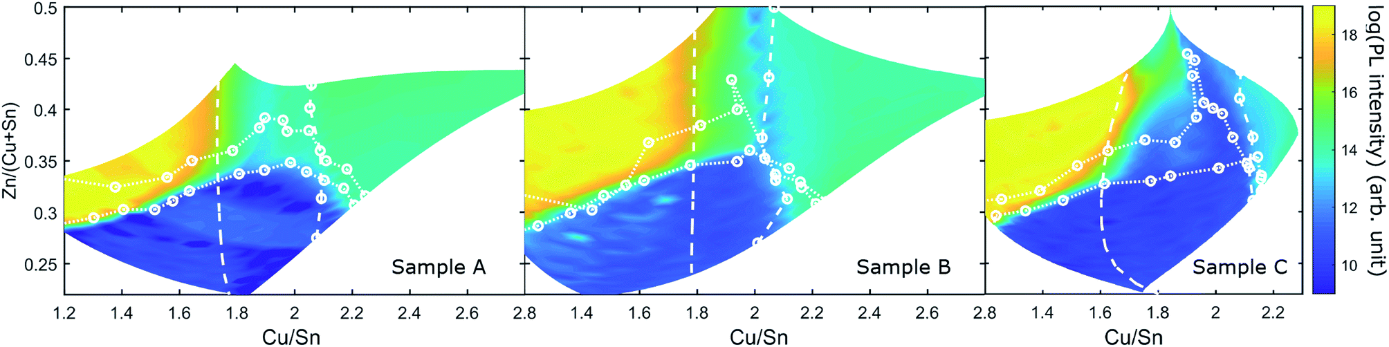 | ||
| Fig. 9 Map of the logarithm of the integrated PL intensity of samples A, B and C. The secondary phase boundaries determined from Raman and XRD are shown as white dotted and dashed lines. | ||
For the remaining regions – including the SPR – the PL intensity is intermediate, being similar in the Zn-rich and Cu-rich parts, with a dip near the line Cu/Sn = 2 (strongest in B and C). It is also noted that the highest PL intensities reach very similar values among the three samples.
The PL intensity within the SPR is essentially flat in all samples, with minor increases towards the Sn-rich side. The highest PL intensity in the SPR is found in sample B (2 min anneal with S), and the lowest in sample C (13 min with CuS and SnS2), in any case it is at least four orders of magnitude lower than in the SnSx containing regions.
Intriguingly, the primary effect of the different anneal conditions on PL is connected to the movement of the phase boundaries. In sample C, the SPR is “stretched” on the Cu/Sn axis, with the SnSx and CuS boundaries being pushed outwards, but the PL intensity variations still follow the boundaries closely. The main difference is that a new region of much lower PL intensity is opened up within the SPR.
These results offer a startling conclusion: the radiative recombination efficiency in CZTS, which might be supposed to be governed by the concentration of deep defects in the CZTS phase, is largely insensitive to the CZTS cation composition. This could be because several different defects or defect complexes create detrimental effects in different composition ranges, or simply because the formation energy of the responsible defect(s) is not influenced by cation composition. On the other hand, the composition of the anneal atmosphere did influence the PL intensity in the single-phase region to some degree, which suggests that the responsible defects are at least partly influenced by the chemical potentials of the gaseous components S and Sn (as SnS(g)).
There are several candidates for defect types which might be independent of cation composition but dependent on the gas phase. The surface and back contact reactions may introduce defects (as well as e.g. metallic CuSx particles) at interfaces. These processes should occur largely irrespective of cation composition; however, both should be supressed by the presence of SnS2 phases and a higher partial pressure of S and SnS.35 Other composition-independent defects include morphological ones (e.g. dislocations or twin boundaries39). The existence of morphological defects in the stoichiometric and Sn-poor areas of the CS samples was indeed hinted at in the TEM images (Fig. 6). A further composition-independent candidate that has received much attention is Cu–Zn disorder in the CZTS phase.
To examine the potential role of Cu–Zn disorder, resonant Raman spectroscopy maps of the CZTS phase were measured. The secondary order parameter Q can be extracted from the resonant Raman spectra by taking the ratio of the peak heights of the Raman modes at 289 cm−1 and 305 cm−1.40 The parameter has been used before to study the crystal quality and cation disorder in CZTS;17,41 high Q correlates to a greater degree of Cu–Zn order. Fig. 10 displays the Q parameter obtained for A, B and C. In the ESI (Fig. S15†), a comparable map of the CZTS main mode width, which is an independent measure of crystal quality, is shown for sample C. Samples A, B and C show several similarities in the dependence of the Q parameter on the cation composition. Q is smallest in the Zn-poor region where Cu3SnS4 exists, and along the Cu/Sn = 2 line. The Q parameter also increases away from the Cu/Sn = 2 line for both Cu-rich and Sn-rich compositions. There are also several differences. Sample A stands out with an overall low Q-parameter. It has its highest values in the Cu-rich CZTS region where the secondary phase CuS is present. This was also observed in our previous studies with CS CZTS samples.17,24 In sample B, the Q parameter in the composition region Cu/Sn < 2 is increased compared to sample A and reaches values similar as in the region Cu/Sn > 2. Moreover, a new region with very high Q appears in the phase region where only SnSx is present alongside CZTS, and also extends inside the SPR. Sample C is similar in this respect, with a further increase in Q in the Sn-rich region as well as in the SPR. Specifically, the variation of Q inside the SPR is confirmation that the CZTS phase composition is changing there. As predicted in ref. 24, higher partial pressures of SnS and S, as in sample B and especially sample C, result in greater off-stoichiometry in the CZTS phase, and ultimately enhance the ordering kinetics due to defect assisted diffusion.17
 | ||
| Fig. 10 Q parameter of sample A, B and C determined from resonant Raman spectra. The secondary phase boundaries determined from Raman and XRD are shown as white dotted and dashed lines. | ||
The Q maps show obvious differences to the PL maps. As far as Q is concerned, the position of the SnSx phase boundary has no effect. Moreover, Q varies considerably inside the SPR for both B and C. Fig. 10 shows that the order parameter is strongly affected by both cation composition and by the annealing conditions across the whole sample and especially inside the SPR, instead of being dominated by the presence of secondary phases as was the case for the PL measurements. The clear conclusion from this comparison is that the changes we observe among the samples in Q and PL must have different origins, i.e. the degree of order in the CZTS phase has little or no influence on the pattern of PL intensity. Again, this is obvious from CS samples but would have been difficult to clarify so directly in another way.
4 Summary
In summary, the results from our CS samples indicate the following trends: the PL intensity, which is an indication of photovoltaic quality, is strongly dependent on the presence of secondary phases and essentially independent of the composition of the CZTS phase. It is rather low in the CZTS single-phase region, although somewhat dependent on the annealing atmosphere (S and SnS partial pressures). However, it is strongly enhanced when SnSx phases are present and quenched when Cu3SnS4 is present. Meanwhile, the presence of ZnS and CuS phases seem to have little or no effect. In terms of morphology, lower densities of morphological defects and a larger grain size were obvious for compositions where SnSx was present. Changing the anneal atmosphere caused the positions of phase boundaries to change, but the PL variations remained attached to the phase boundaries, and the magnitude of the PL signals in the various phase regions was essentially the same in each case, apart from inside the SPR. Increasing the size of the single-phase region by enhancing the SnS and S pressures only reduced the magnitude of its PL signal. Finally, the degree of Cu–Zn order, while strongly affected by CZTS phase composition as well as the annealing conditions, had no influence on the PL signal. In the following, we attempt to provide an explanation for some of these features.First, the impact of Cu3SnS4, which appears to form a solid solution with CZTS, could be attributed to several influences. In Cu3SnS4, Cu appears in (I) and (II) oxidation states whereas in CZTS it only appears in the (I) oxidation state. The phase Cu3SnS4 was reported to be highly p-doped which results in the compound behaving as a metal.42 Defects associated with the change in oxidation state or the inclusion of metallic centres could both be responsible for the overall low PL intensity observed over the whole region with Cu3SnS4 phase.
The enhancement of PL signal by SnSx phases is not due to direct luminescence from this phase: the PL peak is always occurring at 1.3–1.4 eV and is attributable to CZTS. Three possible reasons for the enhancement are considered: (a) interface or grain boundary passivation, (b) modification of the CZTS growth process and (c) suppression of surface and interface decomposition reactions of CZTS.
Concerning passivation by SnSx, such an effect has been shown in some cases (specifically for SnS at the back contact43). However, in the present case this explanation can almost be dismissed because the phase type, morphology and distribution of the SnSx was very different in the three investigated samples, based on TEM-EDX and XRD analysis. It is difficult to believe that identical passivation effects, leading to identical magnitude of CZTS PL, could arise regardless of the location and phase of the SnSx.
In terms of modification of the CZTS growth process, it is plausible that the presence of SnSx phases could enhance diffusion during growth, due to the ion channels formed by the layered structure of SnS and SnSx. Indeed, there was a good correlation between the presence of SnSx phases and the appearance of larger grains with fewer apparent morphological defects (twin boundaries or stacking faults). If such features were to cause recombination, as has been proposed recently,39 PL would be enhanced in their absence.
Finally, the very presence of SnSx during growth is expected to suppress CZTS decomposition processes. Decomposition at the surface and back contact occurs as follows:

In the presence of SnS or SnS2, alternative reactions will occur more easily, protecting the CZTS phase from decomposition or allowing it to “heal” by reabsorbing Sn and S:
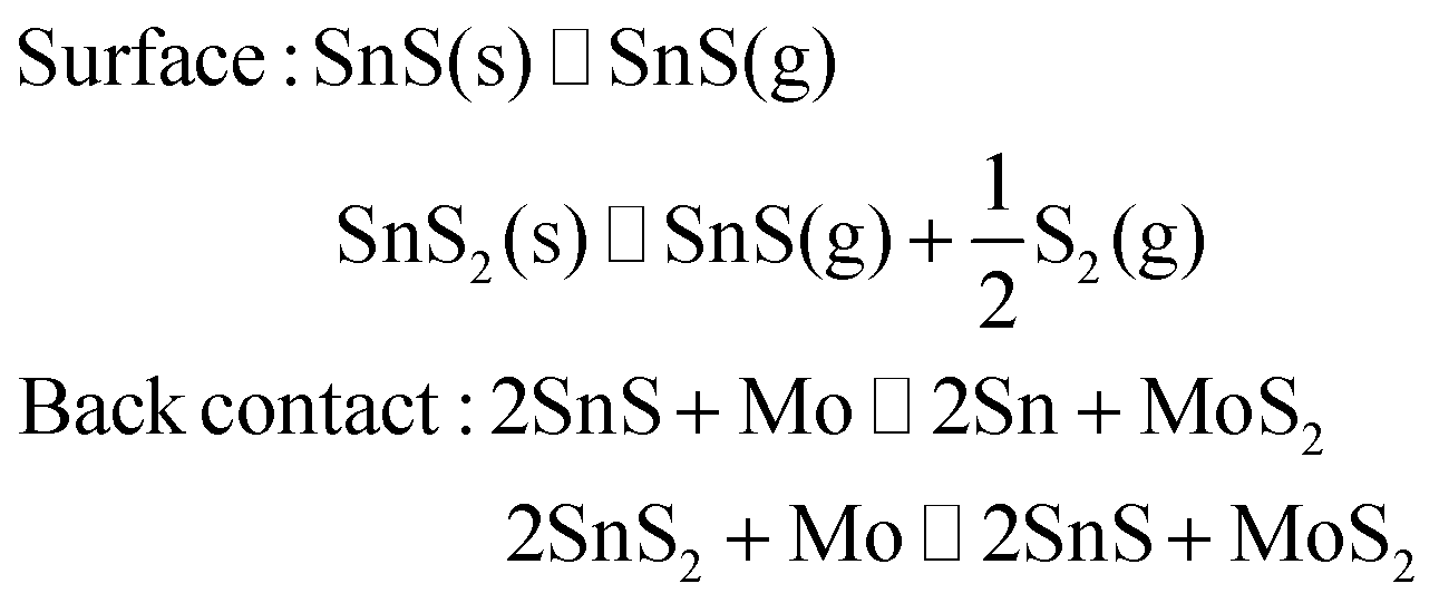
Besides creation of secondary phase particles, the S-deficit induced by the decomposition reactions may lead to “killer” S-vacancy defects11 and thereby to a reduction of PL intensity. The decomposition reactions are essentially composition-independent. However, the suppression reactions can only occur in the presence of excess SnSx phases. Indications of the back contact reaction were seen even for Sn-rich parts of sample A, by STEM-EDX. Therefore the evidence most strongly points to either the surface reaction or to morphological defects (which may even be related39) as being responsible for the poor PL in single-phase CZTS, and the improvement observed when going Sn-rich.
While we show an important role of SnSx secondary phases on CZTS growth and properties, the exact mechanisms are still to be clarified. Meanwhile, it is of concern that secondary phases are apparently needed in order for highest photovoltaic quality to be reached. Despite beneficial effects on the CZTS growth, the requirement for secondary phase presence could itself be a limitation. On the one hand, SnSx phases could block charge transport43 or cause parasitic absorption or shunt pathways in a device. On the other, the presence of these phases implies that the CZTS phase is saturated with Sn-rich defects, including the suspected deep defect SnZn,11 which could be responsible for the difficulty in bringing CZTS performance to higher levels. In a secondary phase region, “defect engineering” faces great difficulties, because the equilibrium of CZTS with secondary phases acts as a buffer for e.g. composition and process changes (fundamentally, the chemical potentials in the multi-phase regions are constant, meaning that defect formation energies no longer change with composition or gas phase partial pressure).
Thus, the most promising route forward would be to explore other means by which to suppress defect creation in single-phase CZTS. The clues provided by this study, namely, to understand the influence of morphological defects and those attributable to CZTS decomposition reactions, hopefully provide a springboard toward this aim. Meanwhile, the power of the CS approach to capture key relationships between process, composition and material properties is of demonstrable benefit.
5 Conclusions
The investigation of composition-spread (CS) thin films is a useful method to understand the complicated interplay of compositional effects, growth process conditions and material properties for complex compounds such as the photovoltaic semiconductor Cu2ZnSnS4 (CZTS). In this contribution we further developed methods for phase identification in CS CZTS films at macro and micro-scales. We used the CS approach to study the effect of very different annealing conditions on CZTS properties, such as the range of the single-phase region, type and distribution of secondary phase formation, photoluminescence (PL) intensity and the degree of cation order. We observe that while the chosen annealing conditions affect the phase stability of CZTS, the size of the single-phase region and the degree of cation ordering, the main factor influencing PL from CZTS is the presence of SnSx and Cu3SnS4 secondary phases, with all samples showing similar trends over their composition ranges. The secondary phase Cu3SnS4 has a detrimental effect on the PL, attributed to formation of a solid solution. However, SnSx secondary phases strongly enhance the CZTS PL intensity. Although SnSx inclusion varies among the three samples in its crystallographic phase and distribution within the CZTS film, it always goes hand-in hand with improved crystal quality of CZTS and a much stronger PL signal. The enhancement by secondary phases clearly implies that, in their absence, CZTS hosts detrimental defects. Since there was no strong composition effect on PL in the CZTS single-phase region, and only a weak effect of process conditions, the evidence points to a defect type whose formation energy is independent of cation composition. Candidates include defects formed via anion deficiency, such as S vacancies created in surface/interface reactions, or morphological defects residing at e.g. grain boundaries, twin boundaries, stacking faults etc. At the same time, Cu–Zn disorder was ruled out as the cause of low PL as a function of composition. The results spell challenges for defect engineering in CZTS. Taking the route where SnSx secondary phases are involved, modification of the CZTS properties will be difficult due to pinning of defect formation energies, while the CZTS phase will be saturated in Sn-rich defects including SnZn. Meanwhile, the possible detrimental impacts of secondary phases need to be examined closely. Taking the single-phase route, we need to understand and tackle a deep defect which is largely independent of composition, being either morphological in nature or due to anion deficiency. Further work with CS samples should focus in more detail on the influence of the gas phase conditions during CZTS synthesis, and explore ways to quantify the impact of morphological defects.Conflicts of interest
There are no conflicts to declare.Acknowledgements
The authors gratefully acknowledge the Göran Gustafsson Foundation (grant no. 1927), the Swedish Research Council (2017-04336), the Swedish Foundation for Strategic Research (SSF, contract RIF14-0053), the strategic research area STandUP for Energy for funding this research. CPB thanks the Swedish Foundation for Strategic Research framework project (RMA15-0030).Notes and references
- A. Bhutani, X. Zhang, P. Behera, R. Thiruvengadam, S. E. Murray, A. Schleife and D. P. Shoemaker, Chem. Mater., 2020, 32, 326–332 CrossRef CAS.
- W. Sun, C. J. Bartel, E. Arca, S. R. Bauers, B. Matthews, B. Orvañanos, B.-R. Chen, M. F. Toney, L. T. Schelhas, W. Tumas, J. Tate, A. Zakutayev, S. Lany, A. M. Holder and G. Ceder, Nat. Mater., 2019, 18, 732–739 CrossRef CAS PubMed.
- H. Park, R. Mall, F. H. Alharbi, S. Sanvito, N. Tabet, H. Bensmail and F. El-Mellouhi, J. Phys. Chem. A, 2019, 123, 7323–7334 CrossRef CAS PubMed.
- D. H. Fabini, M. Koerner and R. Seshadri, Chem. Mater., 2019, 31, 1561–1574 CrossRef CAS.
- Y. Cai, W. Xie, Y. T. Teng, P. C. Harikesh, B. Ghosh, P. Huck, K. A. Persson, N. Mathews, S. G. Mhaisalkar, M. Sherburne and M. Asta, Chem. Mater., 2019, 31, 5392–5401 CrossRef CAS.
- G. Brunin, F. Ricci, V.-A. Ha, G.-M. Rignanese and G. Hautier, npj Comput. Mater., 2019, 5, 63 CrossRef.
- L. H. Wong, A. Zakutayev, J. D. Major, X. Hao, A. Walsh, T. K. Todorov and E. Saucedo, J. Phys.: Energy, 2019, 1, 032001 Search PubMed.
- M. A. Green, E. D. Dunlop, J. Hohl-Ebinger, M. Yoshita, N. Kopidakis and A. W. Ho-Baillie, Prog. Photovoltaics, 2020, 28, 3–15 Search PubMed.
- S. Siebentritt, G. Rey, A. Finger, D. Regesch, J. Sendler, T. P. Weiss and T. Bertram, Sol. Energy Mater. Sol. Cells, 2016, 158, 126–129 CrossRef CAS.
- J. E. Moore, C. J. Hages, R. Agrawal, M. S. Lundstrom and J. L. Gray, Appl. Phys. Lett., 2016, 109, 021102 CrossRef.
- S. Kim, J.-S. Park and A. Walsh, ACS Energy Lett., 2018, 3, 496–500 CrossRef CAS.
- J. J. S. Scragg, J. K. Larsen, M. Kumar, C. Persson, J. Sendler, S. Siebentritt and C. Platzer Björkman, Phys. Status Solidi B, 2016, 253, 247–254 CrossRef CAS.
- M. Grossberg, J. Krustok, C. J. Hages, D. M. Bishop, O. Gunawan, R. Scheer, S. M. Lyam, H. Hempel, S. Levcenco and T. Unold, J. Phys.: Energy, 2019, 1, 044002 Search PubMed.
- X. Liu, Y. Feng, H. Cui, F. Liu, X. Hao, G. Conibeer, D. B. Mitzi and M. Green, Prog. Photovoltaics, 2016, 24, 879–898 Search PubMed.
- A. Lafond, L. Choubrac, C. Guillot-Deudon, P. Deniard and S. Jobic, Z. Anorg. Allg. Chem., 2012, 638, 2571–2577 CrossRef CAS.
- G. Gurieva, L. E. Valle Rios, A. Franz, P. Whitfield and S. Schorr, J. Appl. Phys., 2018, 123, 161519 CrossRef.
- K. Rudisch, A. Davydova, C. Platzer-Björkman and J. Scragg, J. Appl. Phys., 2018, 123, 161558 CrossRef.
- P. Fahey, P. Griffin and J. Plummer, Rev. Mod. Phys., 1989, 61, 289–384 CrossRef CAS.
- R. Klenk, T. Walter, H.-W. Schock and D. Cahen, Adv. Mater., 1993, 5, 114–119 CrossRef CAS.
- J. D. Major, Semicond. Sci. Technol., 2016, 31, 093001 CrossRef.
- C. G. Van de Walle and J. Neugebauer, J. Appl. Phys., 2004, 95, 3851–3879 CrossRef CAS.
- W. F. Maier, K. Stöwe and S. Sieg, Angew. Chem., Int. Ed., 2007, 46, 6016–6067 CrossRef CAS PubMed.
- P. Schöppe, G. Gurieva, S. Giraldo, G. Martínez-Criado, C. Ronning, E. Saucedo, S. Schorr and C. S. Schnohr, Appl. Phys. Lett., 2017, 110, 043901 CrossRef.
- A. Davydova, K. Rudisch and J. J. S. Scragg, Chem. Mater., 2018, 30, 4624–4638 CrossRef CAS.
- A. Nagoya, R. Asahi, R. Wahl and G. Kresse, Phys. Rev. B: Condens. Matter Mater. Phys., 2010, 81, 113202 CrossRef.
- J. J. Scragg, T. Ericson, T. Kubart, M. Edoff and C. Platzer-Björkman, Chem. Mater., 2011, 23, 4625–4633 CrossRef CAS.
- A. D. Collord, H. Xin and H. W. Hillhouse, IEEE J. Photovolt., 2015, 5, 288–298 Search PubMed.
- J. K. Larsen, F. Larsson, T. Törndahl, N. Saini, L. Riekehr, Y. Ren, A. Biswal, D. Hauschild, L. Weinhardt, C. Heske and C. Platzer-Björkman, Adv. Energy Mater., 2019, 9, 1900439 CrossRef.
- A. J. Jackson, D. Tiana and A. Walsh, Chem. Sci., 2016, 7, 1082–1092 RSC.
- Y. Ren, N. Ross, J. K. Larsen, K. Rudisch, J. J. S. Scragg and C. Platzer-Björkman, Chem. Mater., 2017, 29, 3713–3722 CrossRef CAS.
- D. J. Vaughan, Mineral Chemistry of Metal Sulfides, Cambridge University Press, 1978 Search PubMed.
- K. Rudisch, Y. Ren, C. Platzer-Björkman and J. Scragg, Appl. Phys. Lett., 2016, 108, 231902 CrossRef.
- C. G. Munce, G. K. Parker, S. A. Holt and G. A. Hope, Colloids Surf., A, 2007, 295, 152–158 CrossRef CAS.
- M. Kumar, A. Dubey, N. Adhikari, S. Venkatesan and Q. Qiao, Energy Environ. Sci., 2015, 8, 3134–3159 RSC.
- J. J. Scragg, T. Kubart, J. T. Wätjen, T. Ericson, M. K. Linnarsson and C. Platzer-Björkman, Chem. Mater., 2013, 25, 3162–3171 CrossRef CAS.
- W. Zalewski, R. Bacewicz, J. Antonowicz, A. Pietnoczka, T. Evstigneeva and S. Schorr, J. Alloys Compd., 2010, 492, 35–38 CrossRef CAS.
- P. A. Fernandes, P. M. P. Salomé and A. F. da Cunha, J. Phys. D: Appl. Phys., 2010, 43, 215403 CrossRef.
- O. D. Miller, E. Yablonovitch and S. R. Kurtz, IEEE J. Photovolt., 2012, 2, 303–311 Search PubMed.
- K. Leifer, European Kesterite Workshop, Uppsala, 21 November 2019 Search PubMed.
- M. Paris, L. Choubrac, A. Lafond, C. Guillot-Deudon and S. Jobic, Inorg. Chem., 2014, 53, 8646–8653 CrossRef CAS PubMed.
- J. J. S. Scragg, L. Choubrac, A. Lafond, T. Ericson and C. Platzer-Björkman, Appl. Phys. Lett., 2014, 104, 041911 CrossRef.
- V. R. M. Reddy, M. R. Pallavolu, P. R. Guddeti, S. Gedi, K. K. Y. B. Reddy, B. Pejjai, W. K. Kim, T. R. R. Kotte and C. Park, J. Ind. Eng. Chem., 2019, 76, 39–74 CrossRef.
- Y. Ren, M. Richter, J. Keller, A. Redinger, T. Unold, O. Donzel-Gargand, J. J. S. Scragg and C. Platzer Björkman, ACS Energy Lett., 2017, 2, 976–981 CrossRef CAS.
Footnote |
| † Electronic supplementary information (ESI) available. See DOI: 10.1039/d0ta02598d |
| This journal is © The Royal Society of Chemistry 2020 |