
 Open Access Article
 This Open Access Article is licensed under a
 Creative Commons Attribution 3.0 Unported Licence
High-temperature decomposition of Cu2BaSnS4 with Sn loss reveals newly identified compound Cu2Ba3Sn2S8†
José A.
Márquez
 *a,
Jon-Paul
Sun
b,
Helena
Stange
a,
Hasan
Ali
c,
Leo
Choubrac
a,
Stefan
Schäfer
a,
Charles J.
Hages
ad,
Klaus
Leifer
c,
Thomas
Unold
a,
David B.
Mitzi
be and
Roland
Mainz
*a
*a,
Jon-Paul
Sun
b,
Helena
Stange
a,
Hasan
Ali
c,
Leo
Choubrac
a,
Stefan
Schäfer
a,
Charles J.
Hages
ad,
Klaus
Leifer
c,
Thomas
Unold
a,
David B.
Mitzi
be and
Roland
Mainz
*a
aHelmholtz-Zentrum Berlin für Materialien und Energie GmbH, Hahn-Meitner-Platz 1, 14109 Berlin, Germany. E-mail: jose.marquez_prieto@helmholtz-berlin.de; roland.mainz@helmholtz-berlin.de
bDepartment of Mechanical Engineering and Materials Science, Duke University, Durham, North Carolina 27708, USA
cDivision of Applied Materials Sciences, Department of Engineering Sciences, Angstrom Laboratory, Uppsala University, SE 752 37 Uppsala, Sweden
dUniversity of Florida, Department of Chemical Engineering, 1006 Center Drive, Gainesville, FL 32611, USA
eDepartment of Chemistry, Duke University, Durham, North Carolina 27708, USA
First published on 28th May 2020
Abstract
The earth-abundant quaternary compound Cu2BaSnS4 is being currently studied as a candidate for photovoltaics and as a photocathode for water splitting. However, the chemical stability of this phase during synthesis is unclear. The synthesis of other quaternary tin–sulphur-based absorbers (e.g., Cu2ZnSnS4) involves an annealing step at high temperature under sulphur gas atmosphere, which can lead to decomposition into secondary phases involving Sn loss from the sample. As the presence of secondary phases can be detrimental for device performance, it is crucial to identify secondary phase chemical, structural and optoelectronic properties. Here we used a combination of in situ EDXRD/XRF and TEM to identify a decomposition pathway for Cu2BaSnS4. Our study reveals that, while Cu2BaSnS4 remains stable at high sulphur partial pressure, the material decomposes at high temperatures into Cu4BaS3 and the hitherto unknown compound Cu2Ba3Sn2S8 if the synthesis is performed under low partial pressure of sulphur. The presence of Cu4BaS3 in devices could be harmful due to its high conductivity and relatively lower band gap compared to Cu2BaSnS4. The analysis of powder diffraction data reveals that the newly identified compound Cu2Ba3Sn2S8 crystallizes in the cubic system (space group I![[4 with combining macron]](https://www.rsc.org/images/entities/char_0034_0304.gif) 3d) with a lattice parameter of a = 14.53(1) Å. A yellow powder of Cu2Ba3Sn2S8 has been synthesized, exhibiting an absorption onset at 2.19 eV.
3d) with a lattice parameter of a = 14.53(1) Å. A yellow powder of Cu2Ba3Sn2S8 has been synthesized, exhibiting an absorption onset at 2.19 eV.
1. Introduction
The installation of photovoltaic modules worldwide has experienced enormous growth and is expected to continue in future years.1 With this expansion, it becomes clear that a major fraction of global electricity generation may ultimately come from photovoltaics (PV). Therefore, it is of interest to discover and develop new absorber materials comprised of earth-abundant elements to further decrease PV module manufacturing prices, without compromising limited earth resources. Cu2BaSnS4 (CBTS) has recently been identified as an earth-abundant semiconductor. CBTS crystallizes in a trigonal structure (P31 space group)2 with a direct bandgap at ∼2.04 eV3 and sharp absorption onset. In this crystal structure, the Cu1+ and Sn4+ cations are tetrahedrally coordinated, whereas the Ba2+ cations are 8-fold coordinated.4 The bandgap of CBTS can be tuned by partially replacing S by Se. Cu2BaSnS4–xSex is able to preserve the crystal structure of CBTS up to ∼75% replacement of S by Se (x ≈ 3), with a reduced bandgap down to ∼1.55 eV.5 For x > 3, Cu2BaSnS4−xSex becomes more stable in an orthorhombic structure (space group Ama2) with a larger bandgap, ultimately reaching 1.72 eV for the pure selenide compound.6 In comparison to the related Cu2ZnSn(S,Se)4 (CZTS) material system, which is plagued by detrimental cation antisite defects,7 CBTS appears to be attractive due to reduced cation disorder upon substitution of Zn by Ba, which has a much larger ionic radius; reduced cation disorder is manifested as a reduction in sub-bandgap absorption in CBTS compared to CZTS. CBTS-related systems have been studied for several applications, such as PV5,6 and photoelectrochemical solar energy conversion.3,8The optoelectronic quality and performance of chalcogenide compound semiconductor devices strongly depend on secondary phases that might coexist with the main phase in the absorber. For the case of CZTS, typically found secondary phases are Cu2−xS, ZnS, Cu2SnS3, SnS, Sn2S3 and SnS2, from which some are more detrimental than others depending on their optoelectronic properties.9 The presence of secondary phases in multinary chalcogenide films can derive from several factors including: (1) an average film chemical composition outside of the single-phase region of the quaternary compound in the phase diagram10 – e.g., the segregation of Cu2−xSe in Cu-rich Cu(In,Ga)Se2 (ref. 11) and of various binary compounds in kesterites;10 (2) the chemical decomposition of the multinary compound driven by an oxidation–reduction process and loss of components into the gas phase, for example, the reduction of Sn4+ to Sn2+ in CZTS leading to the formation of volatile SnS;12 and (3) decomposition of the quaternary compound upon solid-state reaction with another material, e.g. CZTS decomposition into binaries when in contact with Mo.13
The synthesis of polycrystalline chalcogenide films typically involves a high-temperature processing step during which crystal growth occurs. Under these conditions, Sn-containing quaternary chalcogenides can be unstable (as shown for CZTS) and decompose into secondary phases, resulting in the loss of volatile Sn compounds.14 This Sn-loss process has been shown to be detrimental for solar cells and should be avoided by choosing appropriate synthesis conditions.12,15 Beyond secondary phases, the reduction of Sn4+ to Sn2+, associated with deep defects in CZTS, induces strong structural relaxation that may lead to large electron and hole capture coefficients, enhancing non-radiative recombination.16,17 As CBTS also contains Sn, this might also present a problem for the optoelectronic performance of devices fabricated from this compound (even for relatively low concentrations of these defects). To the extent that these defects are important, we expect that anti-site defect concentrations will be sensitive to the growth conditions and final film stoichiometry. To optimize the synthesis conditions for both secondary phases and defects it is crucial to have detailed knowledge of the decomposition mechanisms of the targeted compounds. Experimental determination of the decomposition reactions of these compounds is challenging, and specialised methods—i.e., such as in situ characterization of structure and composition—are required to fully understand the chemistry of these processes.14,18
Here, we fully determine the decomposition reaction of CBTS as a function of temperature and under different reaction atmospheres by a combination of in situ energy-dispersive X-ray diffraction and X-ray fluorescence (EDXRD/XRF) and ex situ transmission electron microscopy (TEM) and energy-dispersive X-ray spectroscopy (EDX).
2. Results and discussion
2.1. Decomposition of CBTS
To assess the stability of CBTS thin films as a function of annealing temperature, we performed two experiments, illustrated in Fig. 1. In the first process, a previously sulfurized CBTS sample was annealed in a closed reactor under saturated sulphur gas conditions, referred to as “S-anneal” in the following discussion. The second process was carried out with a similarly previously sulfurized sample in a reactor with an open valve without additional sulphur added in the system, referred to as “vacuum anneal” in the following discussion (see Experimental methods for additional details). | ||
| Fig. 1 (a) EDXRD/XRF spectra before heating and at 560 °C of the CBTS sample processed with additional sulfur added and a closed reactor (“S-anneal”). The Sn related fluorescence signals (Sn-Kα, Sn-Kβ) do not change in intensity, indicating the absence of Sn loss. (b) EDXRD-XRF spectra before heating and at 560 °C of the CBTS sample annealed without additional S and with the reactor valve opened and being continuously pumped (“vacuum anneal”). The Sn related fluorescence signals decrease in intensity indicating Sn loss from the sample. The green lines indicate the references of the reflections of the CBTS phase with their corresponding Miller indices. A schematic sketch of the reactor conditions for both annealing experiments is shown next to the spectra. | ||
The EDXRD/XRF spectra of the CBTS sample (Fig. 1a) before starting the annealing (blue line) and at the maximum temperature of 560 °C (red line) for the “S-anneal” experiment show only diffraction peaks attributed to the reference lines for the reflections of the CBTS P31 phase (green vertical lines). A shift of the diffraction reflections toward lower photon energies is observed as a result of thermal expansion for the high temperature data. The intensities of the fluorescence signals of Sn and Ba (Sn-Kα, Sn-Kβ, Ba-Kα) at 560 °C (red) are equal to those before annealing (blue). Hence, we conclude that CBTS remains stable and that no Sn loss occurs during the heating in a saturated sulphur atmosphere up to 560 °C (at least over the 20 min timeframe of the dwell at high temperature).
The EDXRD/XRF spectra of the experiment performed with the “vacuum anneal” before the annealing step and at 560 °C are shown in Fig. 1b. Here, in contrast to the previous “S-anneal” case, the intensity of the Sn fluorescence signals is clearly reduced at 560 °C, indicating Sn loss in the sample during annealing. Additionally, a comparison of the diffraction peaks at 560 °C with the green reference lines shows that CBTS (P31) is not present anymore in the sample (Fig. 1b). This result reveals that CBTS, as previously observed for CZTS, decomposes at high temperatures under low sulphur partial pressure conditions. In addition to this observation, new reflections appear in the spectrum at 560 °C, indicating the formation of new phase(s).
To better understand the interplay of the CBTS decomposition and formation of secondary phases during the “vacuum anneal” condition, we analyze time-resolved EDXRD/XRF spectra recorded during processing, as shown in Fig. 2a and b. Three clear regions can be identified in the evolution of the spectra with process time and temperature:
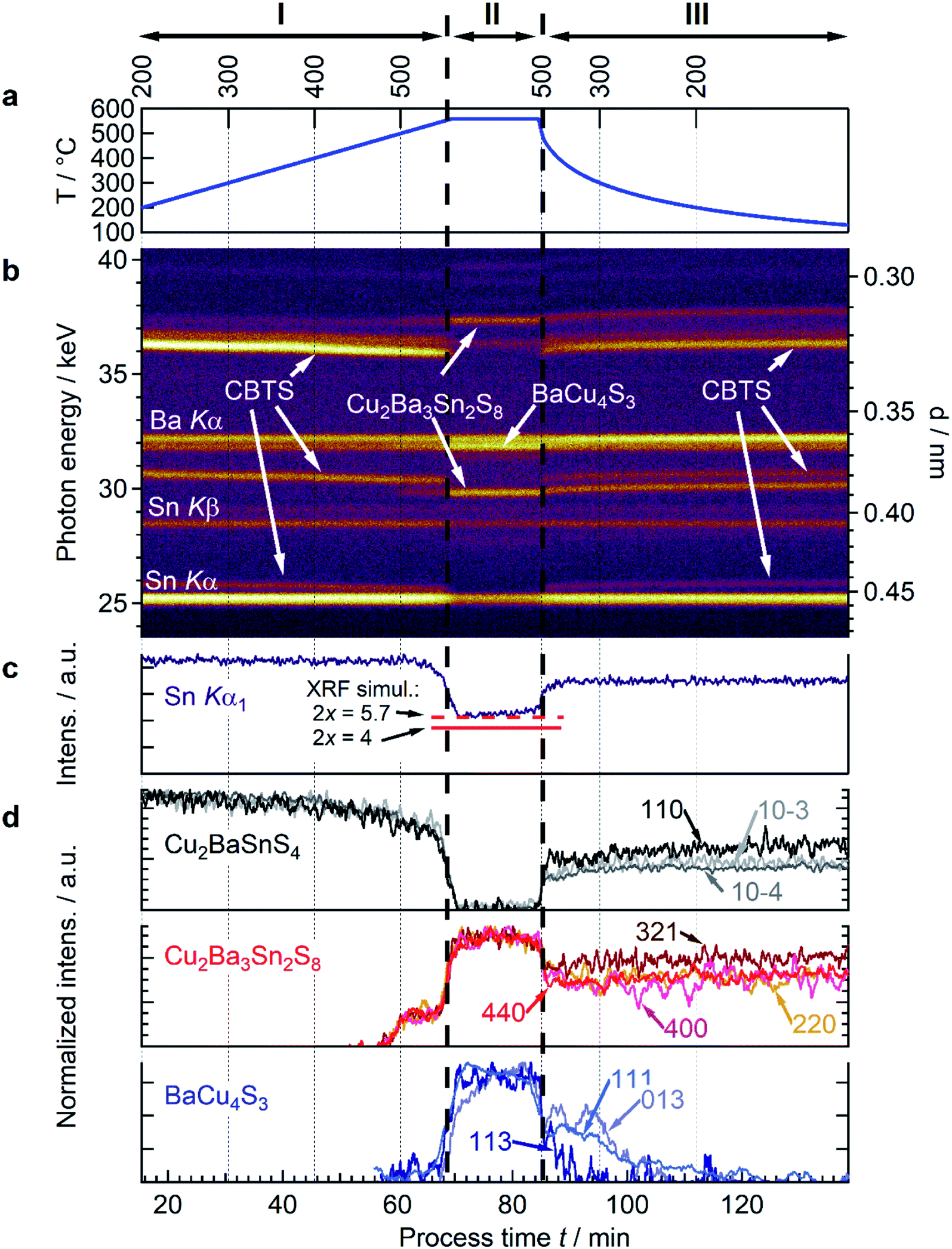 | ||
| Fig. 2 (a) Temperature profile of the annealing process used to study the stability of CBTS (under “vacuum anneal” conditions). Dashed lines are shown as a guide for the temperature values in the top axis. Up to 200 °C a higher heating rate was used to reduce the duration of the measurement. (b) EDXRD/XRF 2D plot as a function of photon energy, lattice spacing d and process time. (c) Integrated intensity of the Sn Kα fluorescence signal. (d) Integrated intensity of the diffraction signals corresponding to the CBTS, Cu2Ba3Sn2S8 and BaCu4S3 phases as a function of the processing time. The numbers (e.g., 110) refer to indices for the different reflections being monitored for the phases in question. | ||
Region I ranges from the beginning of the heating ramp until a temperature of around 540 °C. Here, only the fluorescence peaks of Sn and Ba and the diffraction signals of CBTS (P31) are observed (Fig. 2b). No other secondary phases are identified in this region. A progressive shift of the position of the CBTS diffraction peaks toward lower photon energies is observed as a result of thermal expansion, corresponding to a thermal expansion coefficient of 4.01 × 10⁻⁵ ± 2.5 × 10⁻⁷ K−1 (ESI Fig. S2†).
Region II extends from 540 °C to shortly after the end of the dwelling step at 530 °C (during cooling). Here, the CBTS diffraction signal vanishes and new diffraction signals appear, attributed to the formation of two secondary phases BaCu4S3 and Cu2Ba3Sn2S8. The assignment of BaCu4S3 with a space group Pnma (ICSD 15138) at high temperature is based on a peak match with references from the ICSD crystallographic database (Fig. S1†). Whilst the properties and the crystal structure of BaCu4S3 are documented in literature,19 no report of the phase Cu2Ba3Sn2S8 (or alternatively Ba3Cu2Sn2S8) could be found in literature. The assignment of Cu2Ba3Sn2S8 is based on a combination of the EDXRD spectra and compositional data, as explained in detail below (Sec. 2.2). The increase of the intensity of the diffraction signals of the secondary phases occurs simultaneously with the decrease of the intensity of the CBTS diffraction signals and the decrease of the Sn fluorescence peaks at the transition from Region I to Region II (Fig. 2d). While the CBTS signals completely vanish, the intensity of the Sn fluorescence signals reach a stable level of approximately 50% of its initial value (Fig. 2c). This evolution indicates that the decomposition of CBTS is accompanied by Sn loss, as in CZTS.14,20 For the case of CZTS, the decomposition reaction leads to the formation of Cu–S, ZnS and Sn–S binaries and, in the absence of a sulphur atmosphere, to the complete loss of Sn. However, we find that CBTS decomposes into ternary BaCu4S3 and the quaternary compound Cu2Ba3Sn2S8. Since the latter phase contains Sn and does not further decompose at 560 °C (over the 20 min timeframe of the dwell), Sn loss from the film is constrained, in contrast to the decomposition of CZTS, where Sn is lost completely from the film under the same annealing conditions.
Region III starts shortly after the beginning of the cooling step. An increase of the intensity of the Sn fluorescence peaks is observed in this stage, indicating that some Sn remained in the reactor and is partially reincorporated into the sample during cooling. The increase in the Sn peak intensity during cool-down occurs at around ∼500 ± 30 °C (86 minutes), recovering up to 80% of its initial intensity. As the Sn intensity increases in this region, the peaks associated with CBTS reappear (see Fig. 2c and d). Simultaneously, the diffraction signals of Cu2Ba3Sn2S8 decrease in intensity while the signals of BaCu4S3 disappear. This result suggests that both compounds react with the Sn-containing gas phase, resulting in the formation of CBTS. At the end of the process, only diffraction signals of CBTS and Cu2Ba3Sn2S8 are observed in the spectra.
2.2. Identification of Cu2Ba3Sn2S8 secondary phase
To identify the phases revealed by the in situ EDXRD/XRF data, TEM analysis of the cross-section of the resulting film from the “vacuum anneal” condition was performed. Fig. 3a–d shows the bright field (BF) image, electron diffraction pattern, dark field (DF) and HAADF images of the specimen. The presence of a secondary phase is clearly visible in the DF image. Detailed analysis of the region of interest where both phases co-exist shows that the bright secondary phase in the DF image has a lower Cu content and higher Ba content than the other phase (see Fig. 3e–g). Quantitative analysis of the composition of both regions is shown in Table 1. The composition of the secondary phase is close to the stoichiometry of Cu2Ba3Sn2S8 and the composition of the majority phase is similar to CBTS. | ||
| Fig. 3 (a) Bright-field TEM image of the cross-section of the sample prepared with the “vacuum anneal” condition. (b) Selected area electron diffraction pattern acquired from the region marked by a red circle in (a). A reflection corresponding to a lattice spacing 3.88 Å (attributed to the reflection of Cu2Ba3Sn2S8 at around ∼30 keV in Fig. 2b) is marked with small red circles, which in turn was used to produce the dark field image shown in (c). The dark field image shows a distinct grain of the secondary phase (red arrow). (d) HAADF image of the same region of the sample as shown in (c). The green box shows the region where EDX maps have been prepared for (e) Cu, (f) Ba, and (g) Sn. The dumbbell-shaped region (white dashed line) is Cu-poor and Ba-rich in comparison to the remainder of the sample. | ||
| Element | STEM-EDS secondary phase | Stoichiometric Cu2Ba3Sn2S8 | STEM-EDS majority phase | Stoichiometric Cu2BaSnS4 |
|---|---|---|---|---|
| Cu | 15.5 ± 0.6 | 13.3 | 26.0 ± 0.9 | 25.0 |
| Ba | 21.3 ± 2.2 | 20.0 | 14.1 ± 1.4 | 12.5 |
| Sn | 15.2 ± 1.6 | 13.3 | 13.2 ± 1.3 | 12.5 |
| S | 48.0 ± 1.6 | 53.3 | 46.8 ± 1.6 | 50.0 |
Based on the compositional ratios obtained from the TEM-EDX data, we deduce that a compound with the stoichiometry of Cu2Ba3Sn2S8 is a possible candidate. No reference in literature could be found for Cu2Ba3Sn2S8. However, Tampier synthesized the compound Ag2Sr3Ge2Se8, and reported its structure with a cubic unit cell and lattice parameter a = 14.69 Å and space group I3d.21 We used this structure as an initial model, modified it to the Cu2Ba3Sn2S8 stoichiometry, and scaled the unit cell volume to match the lattice plane distances determined from the EDXRD data. The comparison of simulated XRD patterns for this model shows a good match with the reflections observed in the EDXRD data (ESI Fig. S1a†).
To verify the assignment of this phase, a powder sample was synthesized by combining Cu2S, BaS, SnS, and S in a 1![[thin space (1/6-em)]](https://www.rsc.org/images/entities/char_2009.gif) :3:2:2 ratio and heating to 560 °C (See Experimental methods for additional details). Several additional attempts to synthesize the compound at different temperatures (i.e., 500, 525 and 600 °C) resulted in samples with a larger volume fraction of secondary phases. We also attempted the synthesis of single crystals of this phase using a starting Cu2Ba3Sn2S8 stoichiometry powder with additional binary sulfide reagents added to promote crystal growth.22 For each of these attempts, the resulting samples presented a larger volume fraction of the CBTS phase than for the 560 °C solid-state reaction. Fig. 2 suggests that the Cu2Ba3Sn2S8 phase primarily appears at high temperature. This apparent stability profile seems to hinder both crystal growth, as well as room-temperature single-phase powder formation. The powder diffraction pattern in Fig. 4a is consistent with the presence of the above constructed Cu2Ba3Sn2S8 structure with a space group I3d as the main phase. However, the powder is not single phase and additional reflections can be attributed to CBTS and BaSO4 (Fig. 4a). The origin of the oxygen is currently unknown, but it might arise from an incomplete drying of the quartz tube or from partially oxidized precursors. Assuming these three phases being present, the measured powder pattern could be successfully fitted with the Pawley method (black line in Fig. 4a), resulting in a lattice parameter for Cu2Ba3Sn2S8 of a = 14.53(1) Å.
:3:2:2 ratio and heating to 560 °C (See Experimental methods for additional details). Several additional attempts to synthesize the compound at different temperatures (i.e., 500, 525 and 600 °C) resulted in samples with a larger volume fraction of secondary phases. We also attempted the synthesis of single crystals of this phase using a starting Cu2Ba3Sn2S8 stoichiometry powder with additional binary sulfide reagents added to promote crystal growth.22 For each of these attempts, the resulting samples presented a larger volume fraction of the CBTS phase than for the 560 °C solid-state reaction. Fig. 2 suggests that the Cu2Ba3Sn2S8 phase primarily appears at high temperature. This apparent stability profile seems to hinder both crystal growth, as well as room-temperature single-phase powder formation. The powder diffraction pattern in Fig. 4a is consistent with the presence of the above constructed Cu2Ba3Sn2S8 structure with a space group I3d as the main phase. However, the powder is not single phase and additional reflections can be attributed to CBTS and BaSO4 (Fig. 4a). The origin of the oxygen is currently unknown, but it might arise from an incomplete drying of the quartz tube or from partially oxidized precursors. Assuming these three phases being present, the measured powder pattern could be successfully fitted with the Pawley method (black line in Fig. 4a), resulting in a lattice parameter for Cu2Ba3Sn2S8 of a = 14.53(1) Å.
 | ||
| Fig. 4 a) Powder diffraction pattern of the Cu2Ba3Sn2S8 synthesised sample. The reference patterns of Cu2Ba3Sn2S8, CBTS and BaSO4 are shown below. A Pawley fit (black line Χ2 = 1.89) was performed taking into account the presence of the three phases. Additional unassigned peaks are marked with a star (*). (b) Tauc plot for the bandgap determination of the powder sample assuming a direct bandgap. | ||
2.3. Optical properties of Cu2Ba3Sn2S8 secondary phase
The optical properties of the synthesized powder were evaluated with diffuse reflectance spectroscopy. Evaluation of a Tauc plot (Fig. 4b) using the Kubelka–Munk function23 assuming a direct transition, yields a bandgap of 1.97 eV. This is consistent with the presence of CBTS (as detected in the experimental powder diffraction pattern) for which a bandgap of 2.0 eV has been reported.5 In the diffuse reflectance data, a second, higher absorption feature at 2.19 eV can be extracted. Besides CBTS, the powder diffraction suggests the presence of BaSO4 and Cu2Ba3Sn2S8. Since BaSO4 has a much higher bandgap of 6.0 eV,24 we attribute this second drop in absorption at 2.19 eV to the bandgap of Cu2Ba3Sn2S8.2.4. Decomposition reaction
A plausible reaction mechanism describing the decomposition of CBTS observed in the process with the “vacuum anneal” condition is presented in reaction (1). | (Reaction 1) |
This reaction is consistent with the observed decrease of the Sn Kα signal during the decay of CBTS, as part of the Sn is lost from the sample by evaporation of SnS. The Sn reincorporation observed during the cooling stage additionally proves the reversibility of the formation/decomposition reaction of CBTS from/to Cu2Ba3Sn2S8, BaCu4S, SnS (g), and S2 (g). We note that the actual chemistry of the gas phase products in reaction (1) can not be determined experimentally with precision. This means that the products SnS (g) and S2 (g), could also be replaced by SnS2 (g) in Reaction (1).
To check if this reaction is quantitatively in accordance with the Sn Kα signal decrease by ∼50%, XRF simulations were performed assuming that reaction (2) takes place with a variation of x:
 | (Reaction 2) |
(Note that for a given x there is only one solution for α, β, γ, and δ). An exact match between measurement and simulation is gained with 2x = 5.7. A BaCu5.6S4.5 phase is reported in the literature, but the structure does not agree with the observed EDXRD reflections. The XRF simulations assuming 2x = 4 (i.e., BaCu4S3) results in a 10% larger decrease of the Sn Kα signal (60% compared to the observed 50%, see Fig. 2c). Possible reasons for this discrepancy could be that (a) the initial composition of CBTS was not perfectly stoichiometric or (b) the phases have broad stoichiometric existence regions, which are not considered in reaction (2), for example, Cu-rich BaCu4S3.
2.5. Consequences for CBTS process design
From the knowledge acquired about the decomposition mechanism of CBTS, consequences can be derived for the processing of high-quality thin film absorber layers: similar to CZTS, the sulfurization process or subsequent annealing at high temperatures >500 °C must be performed under high sulphur partial pressure conditions to avoid decomposition and the final presence of secondary phases in the films. With regard to the nature of the secondary phases identified in the decomposition mechanism, BaCu4S3 is likely the most important to be avoided. One reason for the expected negative impact of BaCu4S3 is its narrower bandgap (1.8 eV)19 compared to CBTS (2.04 eV),3 which will ultimately limit the achievable VOC. The second reason is the high conductivity of BaCu4S3, which has been demonstrated for a large compositional space19 and which can be assumed to induce shunting problems if present in the absorber layer. A Cu-poor composition should help to avoid the formation of BaCu4S3 as a secondary phase during film synthesis. Given the wider bandgap of Cu2Ba3Sn2S8 compared to CBTS and assuming no additional recombination at the interface between the two phases, Cu2Ba3Sn2S8 could be less detrimental for the VOC of CBTS devices than BaCu4S3. Further experimental and theoretical studies of earth-abundant Cu2Ba3Sn2S8 are needed to assess whether or not the material may be suitable for a top cell in tandem devices or in photoelectrochemical cells.3. Conclusion
By using in situ EDXRD/XRF under real processing conditions in combination with ex situ TEM and STEM-EDS analysis, we find that CBTS decomposes into BaCu4S3, SnS (g) and the previously unknown compound Cu2Ba3Sn2S8 at high temperature, if the S partial pressure is not sufficiently high. Cu2Ba3Sn2S8 has been identified and synthesized as a dominant phase in powder form for the first time. Our in situ study reveals that this quaternary phase is stable at high temperatures (560 °C) under low sulphur partial pressure conditions. This constrains the total CBTS film Sn-loss to approximately 50% of the original Sn. While the presence of BaCu4S3 should be avoided in CBTS absorbers for photovoltaic applications due to its narrower bandgap and high conductivity, Cu2Ba3Sn2S8 has a wider bandgap (2.19 eV) and therefore may be less detrimental. We suggest a Cu-poor precursor composition to avoid the formation of BaCu4S3 during CBTS synthesis. Further research around the newly synthesized Cu2Ba3Sn2S8 compound is required to validate if it is of interest on its own for possible optoelectronic applications.4. Experimental methods
4.1. CBTS film synthesis
CBTS thin films were deposited onto Mo-coated glass substrates (from Thin Film Devices) via RF magnetron co-sputtering from Cu, BaS, and Sn targets (from AJA), as described in detail by Shin et. al.25 The precursors were sulfurized in a quartz reactor hot plate at 500 °C for 10 minutes leading to polycrystalline CBTS films.264.2. Real-time EDXRD/XRF analysis during annealing
The pre-sulfurised CBTS films were annealed in S vapour inside a cylindrical graphite reaction box (reactor) with an internal volume of ∼430 cm3, placed inside a vacuum chamber27 at the EDDI beamline28 of the BESSY II synchrotron facility.29In situ energy-dispersive X-ray diffraction (EDXRD) and fluorescence (XRF) data were collected in real-time during sulfurization by an energy-dispersive high-purity Ge detector. For the reactive annealing, 400 mg of S pellets were placed in a ceramic crucible next to the sample. The reactor was sealed with a motorised valve at a pressure of ∼5 × 10⁻⁴ mbar (“S-anneal”) or the valve was left open (“vacuum anneal”). Subsequently, the reactor was heated by 4 halogen lamps each above and below the reactor with a total maximum power of 2000 W. The temperature of the processes was controlled and recorded with a thermocouple located 5 mm above the sample. The heating rate was set to 6 K min−1 with a dwelling step at 560 °C for 20 minutes, followed by a natural cool-down. In the “vacuum anneal”, a pressure of ∼3 × 10⁻³ mbar was measured during the high temperature step with a pressure-gauge located at the beginning of the pumping tube outside of the reactor and the heating zone.4.3. Synthesis of Cu2Ba3Sn2Sn8 powders and characterization
For the synthesis of the Cu2Ba3Sn2Sn8 powders, Cu2S, BaS, SnS, and S were combined in a 1:3:2:2 ratio, ground with mortar and pestle, and cold-pressed, all in a N2-filled glovebox. Pellets were sealed under dynamic vacuum (10−6 torr) in fused silica ampules. Ampules were heated at 550 °C for 96 h and rapidly quenched to room temperature. The resulting material was ground, pressed, and annealed under the same conditions three additional times.
Powder X-ray diffraction measurements were carried out using a PANalytical Empyrean diffractometer using Cu Kα radiation under ambient conditions.
Diffuse reflectance measurements were performed with an Enlitech QE-R Spectral Response Measurement System. Bandgaps were determined by transforming the diffuse reflectance spectra with the Kubelka–Munk function,23F(R), defined as F(R) = (1 − R)2/2R, where R is the diffuse reflectance. Direct bandgaps were extracted by determining the onset of absorption from Tauc plots by plotting (F(R))2vs. hν.
4.4. TEM characterization
A cross-sectional TEM sample of the “vacuum anneal” film was prepared by mechanical polishing and Ar ion milling. Dark field (DF) TEM imaging was performed on a 300 kV FEI-Tecnai F30 TEM equipped with a Gatan tridiem energy filter to identify the presence of different phases in the film. A selected area electron diffraction (SAED) pattern was acquired from the films to identify the reflections of the secondary phases. An objective aperture was used to produce the DF image from the selected reflection of the secondary phase. The composition of the secondary phase was then investigated by acquiring the STEM-EDS maps from the region containing a grain of the secondary phase. The EDS-mapping was carried out on a FEI Titan Themis equipped with a probe corrector and a superX EDX detector, operating at an acceleration voltage of 200 kV.Conflicts of interest
There are no conflicts to declare.Acknowledgements
This research was supported by the H2020 programme under the project STARCELL (H2020-NMBP-03-2016-720907). J. P. S and D. B. M thank the U. S. Department of Energy, Office of Science, Basic Energy Sciences (BES), for support under contract DE-SC0020061. J. P. S. thanks the Natural Sciences and Engineering Research Council of Canada for a postdoctoral fellowship.References
- G. Masson and I. Kaizuka, The 23rd International Survey Report on Trends in Photovoltaic PV Applications, 2018 Search PubMed.
- C. L. Teske and O. Vetter, Präparative Und Röntgenographische Untersuchung Am System Cu2−xAgxBaSnS4, Z. Anorg. Allg. Chem., 1976, 426(3), 281–287 CrossRef CAS.
- D. Shin, E. Ngaboyamahina, Y. Zhou, J. T. Glass and D. B. Mitzi, Synthesis and Characterization of an Earth-Abundant Cu2BaSn(S,Se)4 Chalcogenide for Photoelectrochemical Cell Application, J. Phys. Chem. Lett., 2016, 7(22), 4554–4561, DOI:10.1021/acs.jpclett.6b02010.
- T. Zhu, W. P. Huhn, G. C. Wessler, D. Shin, B. Saparov, D. B. Mitzi and V. Blum, I2-II-IV-VI4(I = Cu, Ag; II = Sr, Ba; IV = Ge, Sn; VI = S, Se): Chalcogenides for Thin-Film Photovoltaics, Chem. Mater., 2017, 29(18), 7868–7879, DOI:10.1021/acs.chemmater.7b02638.
- D. Shin, T. Zhu, X. Huang, O. Gunawan, V. Blum and D. B. Mitzi, Earth-Abundant Chalcogenide Photovoltaic Devices with over 5% Efficiency Based on a Cu2BaSn(S,Se)4 Absorber, Adv. Mater., 2017, 29(24), 1–7, DOI:10.1002/adma.201606945.
- D. Shin, B. Saparov, T. Zhu, W. P. Huhn, V. Blum and D. B. Mitzi, BaCu2Sn(S,Se)4: Earth-Abundant Chalcogenides for Thin-Film Photovoltaics, Chem. Mater., 2016, 28(13), 4771–4780, DOI:10.1021/acs.chemmater.6b01832.
- J. J. S. Scragg, L. Choubrac, A. Lafond, T. Ericson and C. Platzer-Björkman, A Low-Temperature Order-Disorder Transition in Cu2ZnSnS4 Thin Films, Appl. Phys. Lett., 2014, 104(4), 041911, DOI:10.1063/1.4863685.
- Y. Zhou, D. Shin, E. Ngaboyamahina, Q. Han, C. B. Parker, D. B. Mitzi and J. T. Glass, Efficient and Stable Pt/TiO2/CdS/Cu2BaSn(S,Se)4 Photocathode for Water Electrolysis Applications, ACS Energy Lett., 2018, 3(1), 177–183, DOI:10.1021/acsenergylett.7b01062.
- S. Siebentritt, Why Are Kesterite Solar Cells Not 20% Efficient?, Thin Solid Films, 2013, 535(1), 1–4, DOI:10.1016/j.tsf.2012.12.089.
- A. Davydova, K. Rudisch and J. J. S. Scragg, The Single Phase Region in Cu2ZnSnS4 Thin Films from Theory and Combinatorial Experiments, Chem. Mater., 2018, 30(14), 4624–4638, DOI:10.1021/acs.chemmater.8b01213.
- R. Mainz, E. Simsek Sanli, H. Stange, D. Azulay, S. Brunken, D. Greiner, S. Hajaj, M. D. Heinemann, C. A. Kaufmann and M. Klaus, et al., Annihilation of Structural Defects in Chalcogenide Absorber Films for High-Efficiency Solar Cells, Energy Environ. Sci., 2016, 9(5), 1818–1827, 10.1039/C6EE00402D.
- J. J. Scragg, T. Ericson, T. Kubart, M. Edoff and C. Platzer-Björkman, Chemical Insights into the Instability of Cu2ZnSnS4 Films during Annealing, Chem. Mater., 2011, 23(20), 4625–4633, DOI:10.1021/cm202379s.
- J. J. Scragg, J. T. Wätjen, M. Edoff, T. Ericson, T. Kubart and C. Platzer-Björkman, A Detrimental Reaction at the Molybdenum Back Contact in Cu2ZnSn(S,Se)4 Thin-Film Solar Cells, J. Am. Chem. Soc., 2012, 134(47), 19330–19333, DOI:10.1021/ja308862n.
- A. Weber, R. Mainz and H. W. Schock, On the Sn Loss from Thin Films of the Material System Cu–Zn–Sn–S in High Vacuum, J. Appl. Phys., 2010, 107(1), 13516, DOI:10.1063/1.3273495.
- A. Redinger, D. M. Berg, P. J. Dale and S. Siebentritt, The Consequences of Kesterite Equilibria for Efficient Solar Cells, J. Am. Chem. Soc., 2011, 133(10), 3320–3323, DOI:10.1021/ja111713g.
- S. Kim, J.-S. Park and A. Walsh, Identification of Killer Defects in Kesterite Thin-Film Solar Cells, ACS Energy Lett., 2018, 3(2), 496–500 CrossRef CAS.
- S. Kim, T. Unold, A. Walsh, J. A. Márquez, T. Unold and A. Walsh, Upper Limit to the Photovoltaic Efficiency of Imperfect Crystals from First Principles, Energy Environ. Sci., 2020, 13(5), 1481–1491 RSC.
- J. Márquez, H. Stange, C. J. Hages, N. Schaefer, S. Levcenko, S. Giraldo, E. Saucedo, K. Schwarzburg, D. Abou-Ras and A. Redinger, et al., Chemistry and Dynamics of Ge in Kesterite: Toward Band-Gap-Graded Absorbers, Chem. Mater., 2017, 29(21), 9399–9406, DOI:10.1021/acs.chemmater.7b03416.
- Y. Han, S. Siol, Q. Zhang and A. Zakutayev, Optoelectronic Properties of Strontium and Barium Copper Sulfides Prepared by Combinatorial Sputtering, Chem. Mater., 2017, 29(19), 8239–8248, DOI:10.1021/acs.chemmater.7b02475.
- J. J. Scragg, T. Ericson, T. Kubart, M. Edoff and C. Platzer-Björkman, Chemical Insights into the Instability of Cu2ZnSnS4 Films during Annealing, Chem. Mater., 2011, 23(20), 4625–4633, DOI:10.1021/cm202379s.
- M. Tampier, Chalkogenogermanate Der Übergangselemente Mit Unedlen Metallen, 2002 Search PubMed.
- J. K. Bao, K. Willa, M. P. Smylie, H. Chen, U. Welp, D. Y. Chung and M. G. Kanatzidis, Single Crystal Growth and Study of the Ferromagnetic Superconductor RbEuFe4As4, Cryst. Growth Des., 2018, 18(6), 3517–3523, DOI:10.1021/acs.cgd.8b00315.
- P. Kubelka, New Contributions to the Optics of Intensely Light-Scattering Materials Part I, J. Opt. Soc. Am., 1948, 38(5), 448, DOI:10.1364/JOSA.38.000448.
- A. Jain, S. P. Ong, G. Hautier, W. Chen, W. D. Richards, S. Dacek, S. Cholia, D. Gunter, D. Skinner and G. Ceder, et al., Commentary: The Materials Project: A Materials Genome Approach to Accelerating Materials Innovation, APL Mater., 2013, 1(1), 011002 CrossRef.
- D. Shin, B. Saparov and D. B. Mitzi, Defect Engineering in Multinary Earth-Abundant Chalcogenide Photovoltaic Materials, Adv. Energy Mater., 2017, 7(11), 1602366 CrossRef.
- J.-P. Sun, J. A. Márquez, H. Stange, R. Mainz and D. B. Mitzi, Phase and Film Formation Pathway for Vacuum-Deposited Cu2BaSn(S,Se)4 Absorber Layers, Phys. Rev. Mater., 2019, 3(5), 055402, DOI:10.1103/PhysRevMaterials.3.055402.
- H. Rodriguez-Alvarez, I. M. Kötschau and H. W. Schock, Pressure-Dependent Real-Time Investigations on the Rapid Thermal Sulfurization of Cu-In Thin Films, J. Cryst. Growth, 2008, 310(15), 3638–3644, DOI:10.1016/j.jcrysgro.2008.05.005.
- C. Genzel, I. A. Denks, J. Gibmeier, M. Klaus and G. Wagener, The Materials Science Synchrotron Beamline EDDI for Energy-Dispersive Diffraction Analysis, Nucl. Instrum. Methods Phys. Res. Sect. A Accel. Spectrom. Detect. Assoc. Equip., 2007, 578(1), 23–33, DOI:10.1016/j.nima.2007.05.209.
- U. Mueller, R. Förster, M. Hellmig, F. U. Huschmann, A. Kastner, P. Malecki, S. Pühringer, M. Röwer, K. Sparta and M. Steffien, et al., The Macromolecular Crystallography Beamlines at BESSY II of the Helmholtz-Zentrum Berlin: Current Status and Perspectives, Eur. Phys. J. Plus, 2015, 130(7) DOI:10.1140/epjp/i2015-15141-2.
Footnote |
| † Electronic supplementary information (ESI) available. See DOI: 10.1039/d0ta02348e |
| This journal is © The Royal Society of Chemistry 2020 |