
 Open Access Article
 This Open Access Article is licensed under a
 Creative Commons Attribution 3.0 Unported Licence
Optical in situ monitoring during the synthesis of halide perovskite solar cells reveals formation kinetics and evolution of optoelectronic properties†
Klara
Suchan
ab,
Justus
Just
 ac,
Pascal
Becker
a,
Eva L.
Unger
bd and
Thomas
Unold
*a
ac,
Pascal
Becker
a,
Eva L.
Unger
bd and
Thomas
Unold
*a
aHelmholtz-Zentrum Berlin für Materialien und Energie GmbH, Structure and Dynamics of Energy Materials, Hahn-Meitner-Platz 1, 14109 Berlin, Germany. E-mail: unold@helmholtz-berlin.de
bChemical Physics and NanoLund, Lund University, Box 124, SE-22100, Lund, Sweden
cMAX IV Laboratory, Lund University, PO Box 118, SE-22100 Lund, Sweden
dHelmholtz-Zentrum Berlin für Materialien und Energie GmbH, Young Investigator Group Hybrid Materials Formation and Scaling, Kekuléstraße 5, 12489 Berlin, Germany
First published on 5th May 2020
Abstract
The formation mechanism and the evolution of optoelectronic properties during annealing of chlorine-derived methylammonium lead iodide (MAPbI3−xClx) are investigated in detail combining in situ and ex situ optical and structural characterization. Using in situ optical reflectometry we are able to monitor the evolution of the MAPbI3−xClx phase as a function of time and processing temperature. The formation kinetics is fitted using an improved Johnson–Mehl–Avrami–Kolmogorov model and a delayed formation of MAPbI3−xClx is found when chlorine is present in the precursor. This is verified by X-ray diffraction and X-ray fluorescence measurements. From absolute photoluminescence measurements we determine the implied Voc during film formation, which exhibits a maximum at a specific time during the annealing process. In conjunction with ex situ time-resolved photoluminescence we deduce a decrease in the net doping density for increased annealing times, while the minority carrier lifetime stays constant. We thus demonstrate the potential of in situ optical spectroscopy to monitor and tailor the electronic properties of hybrid perovskites directly during film growth, which can be easily applied to different growth recipes and synthesis environments.
1. Introduction
Metal-halide perovskite solar cells have risen to fame due to their rapid increase in power conversion efficiency to above 25%,1 which has been achieved by systematic device, compositional2–4 and process engineering.5,6 A growing number of synthesis routes are being reported in the quest to optimize the optoelectronic properties of the perovskite absorber layer.7–9 Especially methylammonium lead iodide has been synthesized by many procedures that often differ in the choice of precursors,10–13 their ratio, and solvents utilized.8,14 Hence preparation protocols become increasingly complex.A deeper understanding of how precursors, intermediates and film preparation conditions determine the optoelectronic quality of the metal halide perovskite materials is crucial to: (1) ensure reproducibility of samples within individual laboratories (2) facilitate the adaptation of synthesis protocols and allow comparison between research laboratories and (3) translate device technology to larger areas.15–19 It has been found that the formation of MAPbI3 competes with decomposition into PbI2 such that there is only a relatively small time-window to achieve pure MAPbI3 without precursor residues or impurity phases such as PbI2.12,20 Obtaining materials with well-defined properties reproducibly is crucial to enable the technological utilization of metal-halide perovskites. Ideally, process monitoring and integrated process control would enable to adjust or terminate annealing when optimal material properties are achieved. Lab-based monitoring tools such as optical monitoring are very fast and thus may allow real-time control.21 Although real-time photoluminescence monitoring during perovskite growth has been reported previously22–24 this has so far not been performed in a realistic device fabrication environment e.g. in a glovebox and, even more importantly, so far neither quantitatively analyzed with respect to the evolution of structural and optoelectronic properties of the growing films.
Several studies have focused on understanding the basic mechanisms during the formation of perovskite films.12,25–30 Among the most investigated processes has been the formation of MAPbI3−xClx involving chloride-containing lead precursors such as PbCl2. This synthesis route results in thin-films with long minority charge carrier diffusion lengths and photoluminescence lifetimes as well as low series resistance and good morphology, comparable to materials grown from pure iodide precursors.31,32 Recently, a record Voc = 1.26 V has been demonstrated using such a synthesis route.13 In contrast to the PbI2-based route, there is no need for additional steps such as an anti-solvent drip. The unique combination of good optoelectronic properties and an easy synthesis protocol makes the process exceptionally well suited for up-scaling approaches. The role of chloride in the growth from chloride-containing precursors has been widely debated in literature. Chloride has been suggested to act as a dopant or trap state passivant to rationalize the longer charge carrier lifetimes and higher mobility.31,33 A photoluminescence microscopy study revealed a correlation between an enhanced Cl-content and the local photoluminescence lifetime in individual grains.34 While chlorine has been confirmed to be present in the precursor phase immediately after spin coating, the chlorine content decreases during annealing by loss of methylammoniumchloride (MACl). The chloride-content in annealed films was found to be only a few percent, varying throughout the depth of the film.30,35–38
The formation process itself and especially the crystalline intermediate phases containing chloride were found to be of significant importance, as they template the growth of large grain-size, oriented and high-quality material. Several studies have been carried out to elucidate the key intermediates and film formation kinetics.25,29,30,32,39–41 Stone et al. identified an intermediate phase as MA2PbClI3, consisting of a columnar structure of lead-iodide-chloride octahedra.28 While in previous studies mainly X-ray diffraction-based methods were applied to describe and monitor the growth process in hybrid perovskite thin films,12,20,28–30,40,41 there has been also a recent study in which solar cell properties were simultaneously monitored during growth, by use of a special device structure with interdigitated back contacts.42 Although this study gives information about the evolution of photovoltaic parameters during the growth of these specialized devices, the concept is not easily transferable to an in situ analysis of the optoelectronic properties of real planar devices.
In contrast, the approach followed in the present study focuses on lab-based in situ monitoring of UV/Vis reflectance and photoluminescence during the formation process in a real processing environment (glove box), which can be applied to any real growth process currently used for planar hybrid perovskite devices. In particular, by contact-less monitoring of the evolution of optoelectronic properties during MAPbI3−xClx film formation we are able to identify distinctively different phases during the film formation process and deduce the kinetics of precursor phase consumption, intermediate phase formation and consumption, as well as final product formation. Ex situ powder X-ray diffraction (XRD) as well as X-ray fluorescence (XRF) measurements on samples after defined annealing times are used to identify intermediate phases and quantify the relative chlorine content in the sample as a function of annealing time. Here we furthermore correlate the evolution of the band-gap and photoluminescence peak emission energy with the concentration of MAPbI3−xClx already formed, the photoluminescence quantum yield (PLQY) as well as photoluminescence lifetime to gain insight into the charge carrier dynamics as a function of annealing time and chlorine content. In particular, the PLQY allows us to directly estimate one of the most relevant photovoltaic parameters, the device open-circuit voltage, during the growth/annealing process. This demonstrates that by in situ optical monitoring of the MAPbI3−xClx formation, an optimal end-point of the annealing process can be defined for specific synthesis procedures, opening the way to further significant improvements of performance and reproducibility of halide perovskite based photovoltaics.
2. Results and discussion
2.1 Monitoring optical properties during growth
To investigate the evolution of the optoelectronic properties during the formation of the perovskite thin-film from the spin-coated precursor solution, the samples were monitored by spectrally-resolved reflectance and photoluminescence (PL) measurements in a realistic glove-box processing environment, as sketched in Fig. 1a. In Fig. 1b, heat maps of the PL and reflectance spectra for a MAPbI3−xClx sample are shown as a function of time during the drying and subsequent annealing process at 100 °C. The synthesis process is further described in the Experimental methods section. The shift of the PL peak energy as obtained from a Gaussian-fit to the individual spectra, and the evolution of the absorption onset as obtained from spectral fitting as described below, are indicated as grey traces in the plot. Already during the drying process at t < 0 min the sample is strongly luminescent with an emission energy close to 1.7 eV. After ramping the temperature up to 100 °C, the luminescence peak position decreases continuously down to 1.6 eV for the fully annealed film. The emission intensity decreases within the first minutes but increases again after around 40 min. At this time the reflectance spectra also start to exhibit a clear absorption edge at 1.6 eV, which increases in energy over time. After the PL intensity goes through a maximum it decreases again after t ∼ 60 min.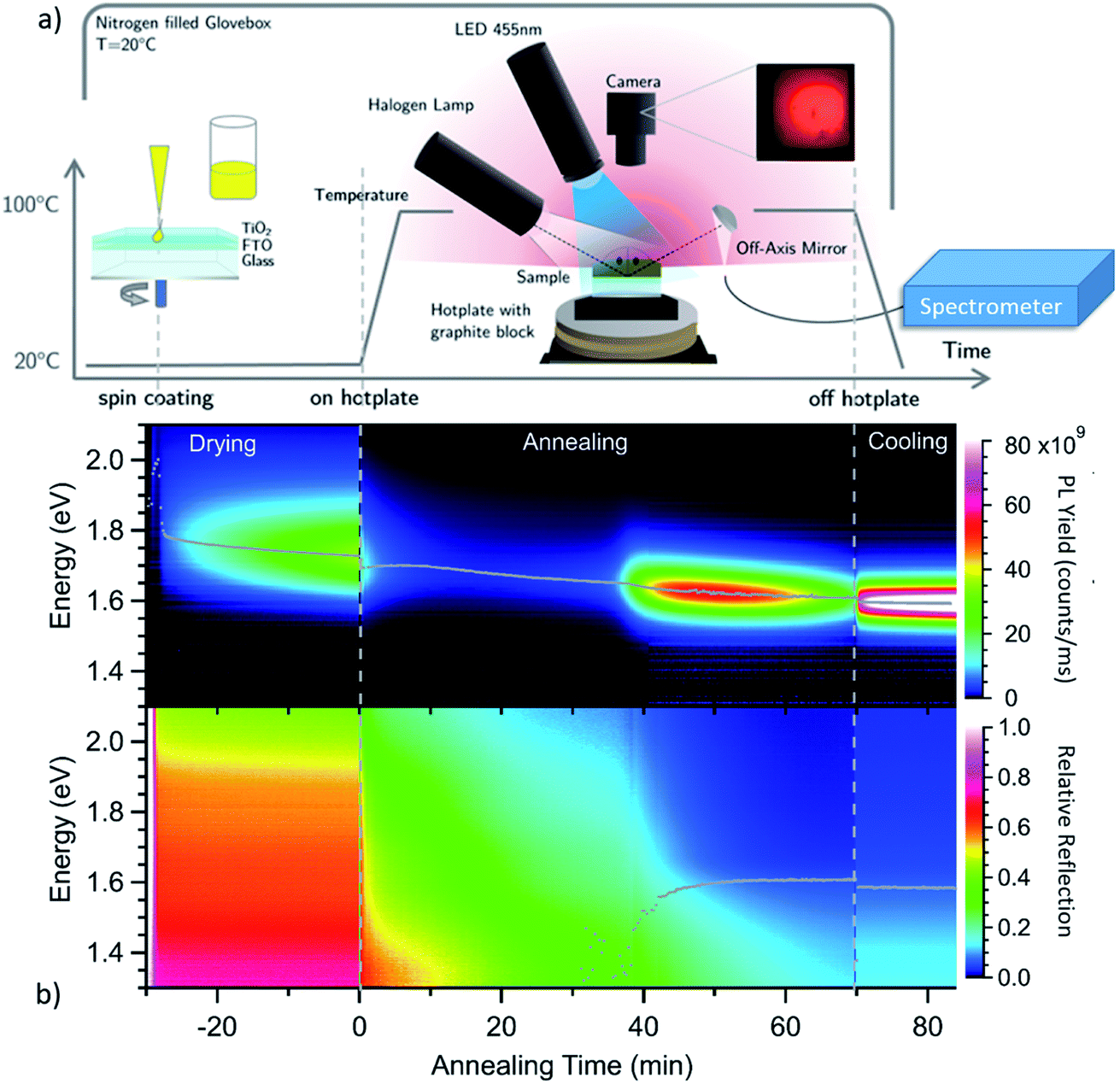 | ||
| Fig. 1 (a) Schematic of the glovebox-based synthesis and optical monitoring process. A camera image of the photoluminescence emitted from the sample after 60 min annealing shown in red colors is shown as an inset. (b) False-color plot of the evolution of photoluminescence (PL) and reflection spectra during the 3-stage synthesis of chlorine derived MAPbI3−xClx. The PL peak energy as well as the energy of the band gap, as obtained from fitting the individual spectra, are superimposed. | ||
To investigate changes in the crystalline phases during the different processing stages, room temperature XRD measurements were performed on samples from process interruptions at defined annealing times of 0 min, 40 min, 45 min, 60 min and 70 min as shown in Fig. 2. Already during the drying stage (t ≤ 0 min), when strong PL emission at 1.7 eV is observed, the XRD pattern shows diffraction peaks from a crystalline phase, in agreement with previous reports.25,28 The XRD pattern exhibits diffraction peaks at 11°, 12°, 15.6°, 16°, 28.5° and 32.7°, which do not agree with those expected for the binary precursor or impurity phases MAI, MACl, PbI2 or PbCl2.
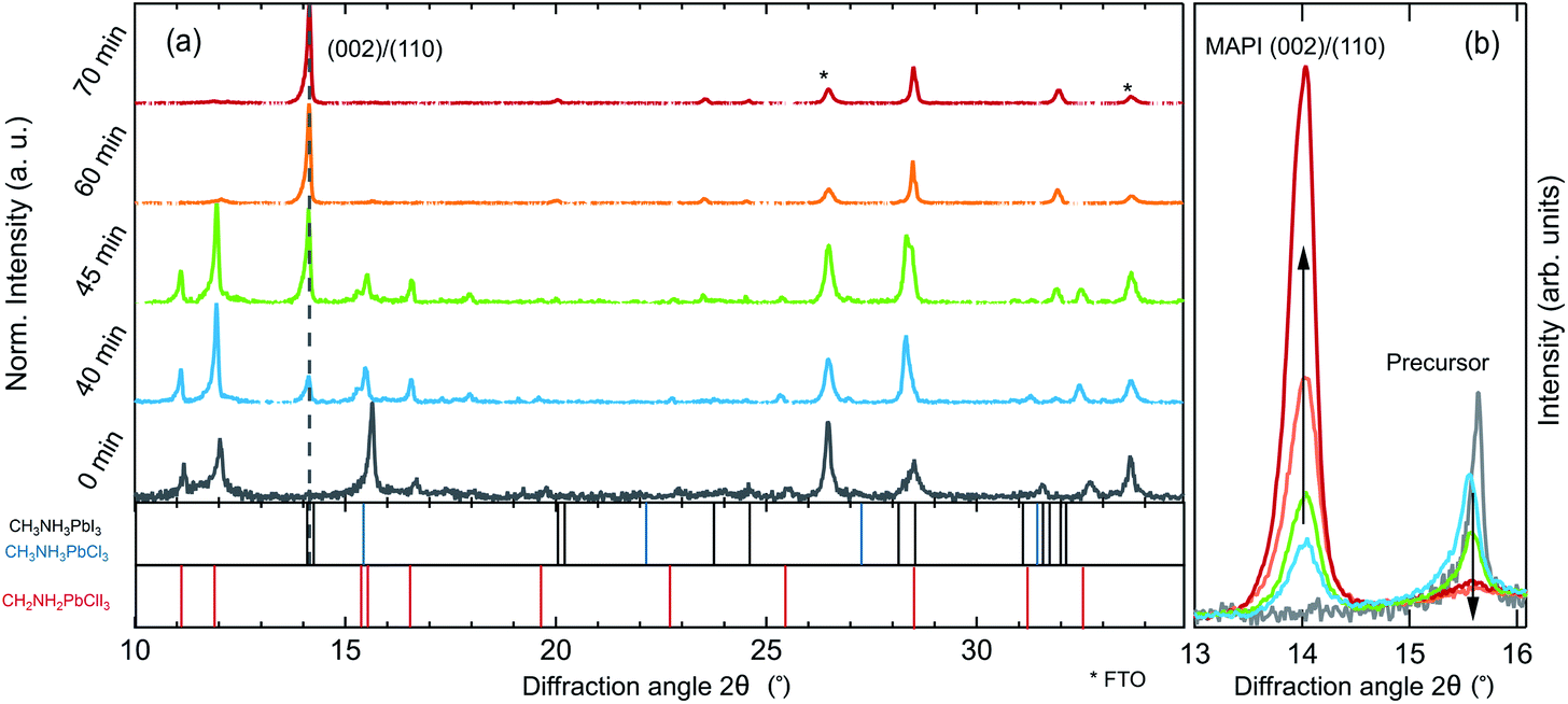 | ||
| Fig. 2 (a) Normalized X-ray diffraction pattern of a MAPbI3−xClx thin-film sample after the drying stage (0 min) as well as after respective times of annealing. The asterisks indicate the diffraction peaks from the FTO/TiO2 substrate. (b) Comparison of the evolution of the MAPbI3−xClx (002)/(110) peak and the precursor peak at 15.6°. | ||
The presence of crystalline precursor phases during annealing and their subsequent decomposition, simultaneously to the formation of MAPbI3 has been discussed for different precursor salts.20,25,27,39 In the case of the PbCl2-derived synthesis route, diffraction peaks comparable with lattice distances in crystalline MAPbCl3 (ref. 25) have led to the conclusion that a pure or chloride-rich methylammonium lead halide perovskite could be a component of the crystalline precursor phase.25,32,43–45 The associated lattice plane distances of the diffraction peaks at 15.6° and 32.7° are indeed consistent with those of MAPbCl3. However, some of the diffraction peaks expected for MAPbCl3, such as the (011) and (022) peaks, are not observed in the powder diffractogram of our samples (see Fig. S1 and S2 in the ESI†). Instead, all diffraction peaks are consistent with a crystalline phase of MA2PbClI3 (ref. 28) which exhibits a similar near-range order but a lower local symmetry than MAPbCl3. In this proposed structure, chloride ions preferentially occupy the axial lattice sites of lead-iodide-chloride octahedra. Therefore, in the [002]-direction, the lattice constant is identical to that of MAPbCl3, resulting in the diffraction peak at 15.6°, which has sometimes been attributed to crystalline MAPbCl3.40,45
During annealing, weak diffraction peaks evolve, that can be assigned to the tetragonal phase of MAPbI3−xClx, while the diffraction peaks of the precursor phase(s) diminish in intensity accordingly. The final film only exhibits peaks corresponding to a pure MAPbI3−xClx phase. A direct comparison of the evolution of the peak at 15.6° attributed to the MA2PbClI3 (310)/(001) precursor and the MAPbI3−xClx (002)/(110) peaks is shown in Fig. 2b. It is noteworthy, that the decrease of the MA2PbClI3 peak occurs in parallel to the evolution of the MAPbI3−xClx peak but at no point in time a solid-solution of both phases exists. It can thus be concluded that the final film is not formed by ion-exchange from MA2PbClI3 but nucleates and grows while consuming the precursor phase.
Photoluminescence and optical reflection signals extracted from the in situ data sets at corresponding annealing times are shown in Fig. 3. The volume fraction of MAPbI3−xClx formed in the film can be estimated from the optical reflection data by employing a Beer–Lambert law based model,21 assuming that light is fully reflected at the silver back mirror and thus transmitted twice through the investigated layer of thickness d:
| R(λ,t) = R0(t) + R1(t)exp[−α(λ,t)2dc(t)] | (1) |
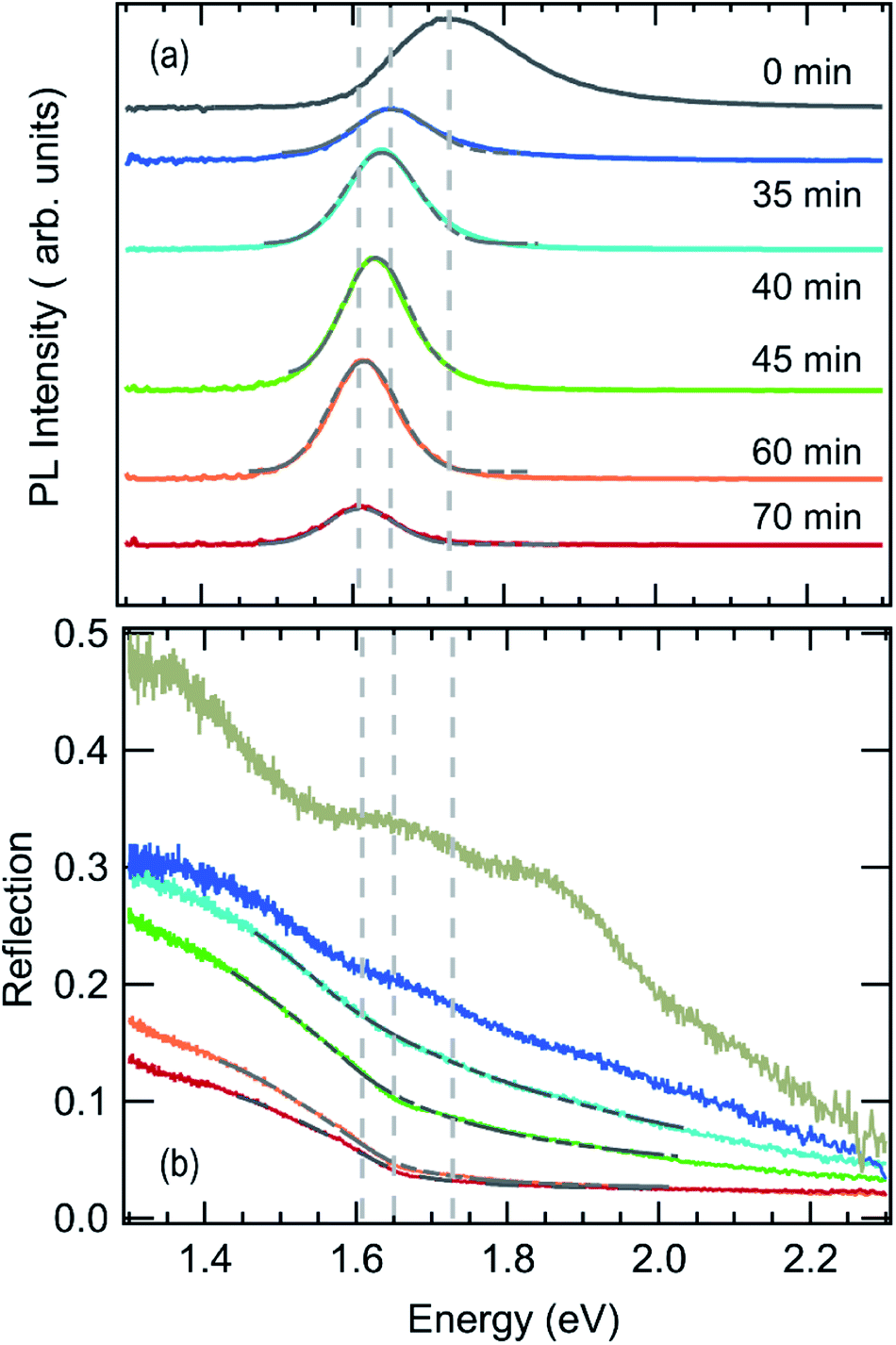 | ||
| Fig. 3 Photoluminescence (a) and white light reflection (b) taken after the drying of the sample at room temperature (grey) and during subsequent annealing at 100 °C. A shift in the photoluminescence peak position as well as the development of an absorption edge are visible. Grey solid lines indicate numerical fits to the data. | ||
No clear absorption edge can be discerned during the initial annealing stage between t = 0 min and t = 35 min. However, the luminescence spectrum of the dried film at t = 0 min, in Fig. 3a, exhibits a peak with a maximum around 1.73 eV and a significantly broadened high energy side.
At about t = 40 min an absorption edge can be recognized in Fig. 3b and the photoluminescence peak redshifts to about 1.6 eV, which agrees with literature values for band-to-band emission of MAPbI3−xClx at 100 °C.47 This is supported by the XRD patterns in Fig. 2a which show an increase of the diffraction peaks corresponding to MAPbI3−xClx between 40 min and 70 min. Thus, we propose that the variable c(t) obtained from fitting the reflection data can be associated with an increasing MAPbI3−xClx volume fraction in the film. Fig. 3 also shows the fits of the reflection spectra indicating that the spectra are well described by the model for annealing times > 35 min. Assuming that at t = 70 min the concentration c = 100% for the fully formed perovskite film with a film thickness of d = 300 nm (compare Fig. S3†), an absorption constant α0 = 1.6 × 105 cm−1 eV−0.5 is derived, which corresponds to an absorption coefficient of α = 2.5 × 104 cm−1 at 1.6 eV. This value is in good agreement with literature values for PbCl2-derived MAPbI3−xClx.48
In Fig. 4 the PL intensity, the PL peak position, the derived MAPbI3−xClx concentration c(t) and the total chlorine content of the film (from XRF) are shown as a function of annealing time. Note that for all ex situ measurements the errors of the individual measurements are very low, whereas a larger uncertainty arises from the sample to sample variation. A comparison of the ex situ measurements and in situ reproducibility for different synthesis runs can be found in the ESI, Fig. S7–S9.† It can be seen in Fig. 4a that although a significant PL yield is present during the whole process, there is a marked increase in PL yield after 40 min followed by a decrease which, will be further analyzed in the following. Correspondingly, the MAPbI3−xClx concentration c(t) obtained from optical reflection measurements (Fig. 4b) shows a sudden increase, agreeing with the increase of the MAPbI3−xClx phase determined from XRD measurements. Thus, the increase in PL yield can be explained by the formation of MAPbI3−xClx. The formation of MAPbI3−xClx does not occur continuously from the beginning of the annealing but only initiates after a certain delay time. This indicates that the formation does not follow a simple first order reaction but is related to a more complex transformation mechanism, as will be discussed further in Section 2.3.
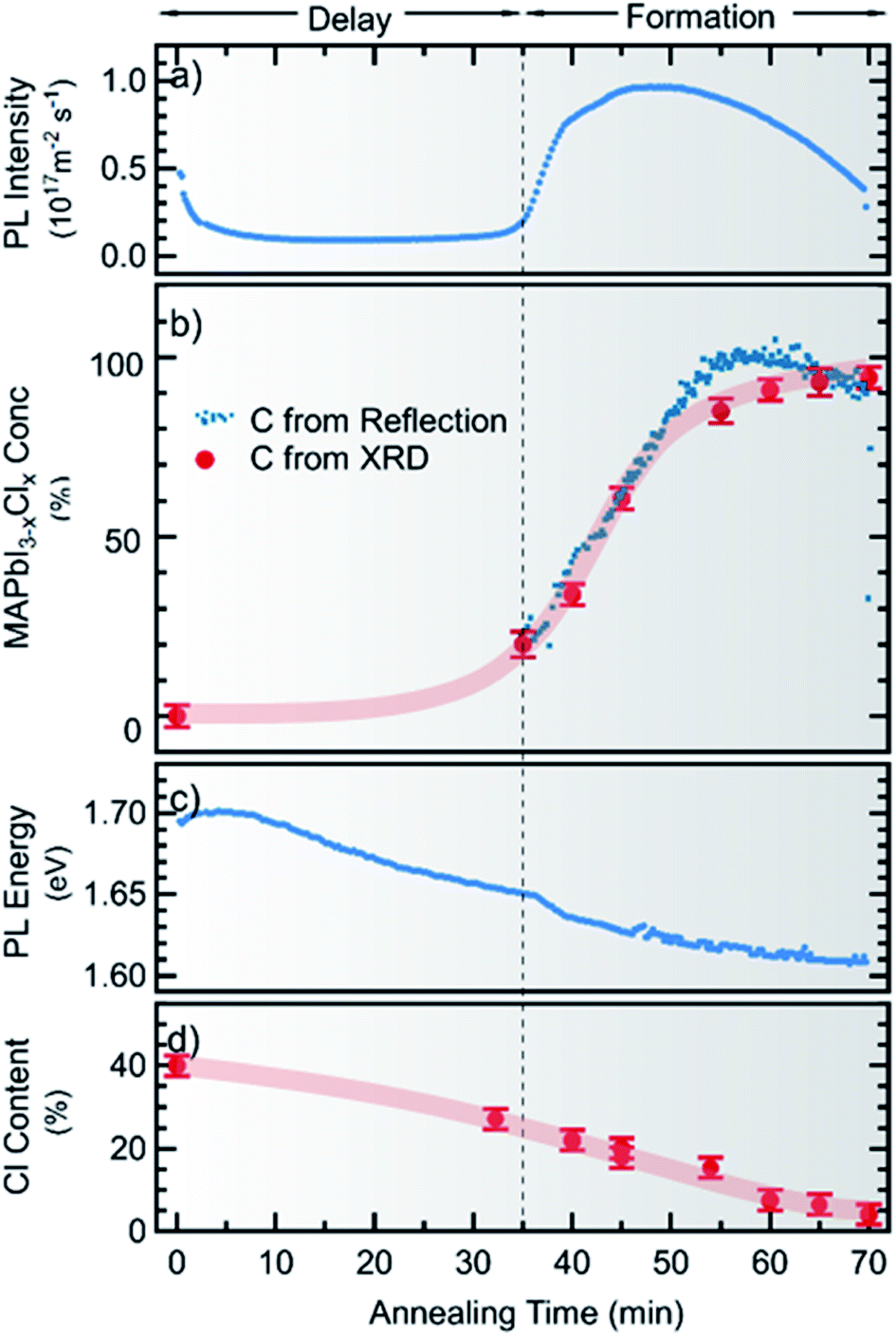 | ||
| Fig. 4 Time evolution of film properties during the annealing stage of the chlorine-derived synthesis of MAPbI3−xClx measured by in situ photoluminescence and reflection spectroscopy as well as ex situ X-ray diffraction and X-ray fluorescence spectroscopy. The obtained photoluminescence intensity is shown in the top panel (a). It can be compared to the concentration of MAPbI3−xClx within the thin film, extracted by fitting the absorption edge of the individual reflection spectra, and the relative reflex height of MAPbI3−xClx measured by X-ray diffraction (b). Furthermore, the PL peak energy (c) is compared to the decrease of the overall chlorine content within the sample, obtained from X-ray fluorescence (d). | ||
From the evolution of the chlorine content determined from XRF measurements (Fig. 4d), it is noted that the onset of the MAPbI3−xClx formation coincides with a loss of about 50% of the initial chlorine content. This observation is consistent with previous studies, which showed that chlorine is released during formation of MAPbI3−xClx from mixed halide precursors.25,28 Our results indicate that no apparent transformation to MAPbI3−xClx occurs before an apparent “excess” of Cl has evaporated during the initial annealing phase. Please note that we did not observe this delay of MAPbI3 formation in a Cl-free processing route using only iodine-containing precursors (see Fig. S10 in the ESI†). This implies that the delay is caused by the presence of (excess) chlorine in the sample.
The PL peak position also shows an interesting behavior: at t = 0 min the maximum is at Epl ∼ 1.7 eV and thus cannot be attributed to pure MAPbI3, which has a bandgap of 1.6 eV at T = 100 °C.47 During the annealing, a red shift can be observed and the PL evolves continuously into the emission consistent with a pure MAPbI3 phase (or MAPbI3−xClx with small x). This continuous redshift is visible during the entire annealing time. This suggests a continuous evolution of the material luminescent at 1.7 eV at t = 0 into the final MAPbI3−xClx phase. In contrast, in XRD the diffraction peaks corresponding to the MAPbI3−xClx phase do not evolve by a continuous peak shift from the observed crystalline precursor phase. The observed luminescent precursor phase must thus be different from the crystalline precursor phase visible in XRD, but possibly arises from MAPbI3−xClx crystallites already present at the beginning of the annealing process, as will be discussed further in Section 2.3.
2.2 Evolution of optoelectronic properties during growth
After about 45 min a decrease in photoluminescence intensity is observed, although the concentration of MAPbI3−xClx is still rising. This clearly indicates a change in the optoelectronic properties of the material. From the photoluminescence signal and the absorbed incident photon flux the photoluminescence quantum yield (PLQY) can be calculated, which is shown in Fig. 5a. It can be seen, that the PLQY first reaches a maximum of 0.14% at about 48 min, and then decreases with further annealing. We note that this value compares well to recent results obtained for perovskite absorber layers yielding more than 20% conversion efficiency in devices,49 in particular when taking into account that the processing (and thus measurement) temperature of 100 °C attenuates the PLQY by approximately a factor of 3 (see ESI, Fig. S11†).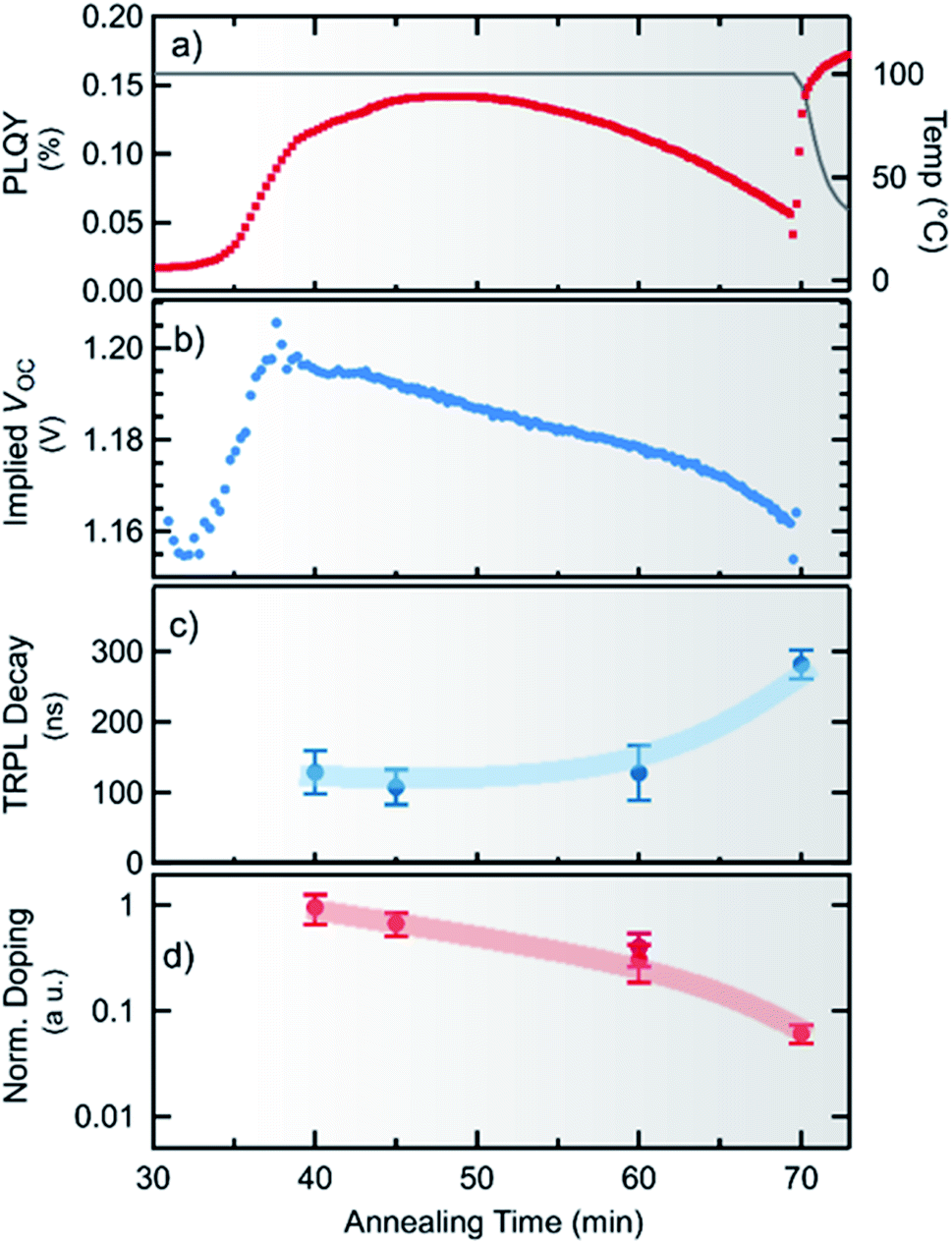 | ||
| Fig. 5 Time evolution of optical properties during the annealing stage of the chlorine-derived synthesis of MAPbI3−xClx obtained from in situ photoluminescence spectroscopy as well as ex situ time-resolved photoluminescence. In (a) and (b), the quantum yield and the implied open circuit voltage (iVoc) during the process are compared. Additionally, the process temperature is shown in grey. In (c) the effective carrier lifetime as measured by TRPL is shown. (d) The normalized doping density estimated from PLQY and TRPL decay time decreases during annealing. | ||
From the temperature-corrected PLQY, the quasi-Fermi level splitting μ (or implied open-circuit voltage iVoc) expected at room temperature can be estimated following the approach of Ross50
μ = μrad + kBT![[thin space (1/6-em)]](https://www.rsc.org/images/entities/char_2009.gif) ln(PLQY/ae) = qiVoc ln(PLQY/ae) = qiVoc | (2) |
To estimate the minority carrier lifetime and possible changes in the charge carrier (doping) density n0 during annealing, time-resolved photoluminescence (TRPL) measurements were performed ex situ after different annealing times. To account for the concentration of MAPbI3−xClx formed after different times, the initial TRPL amplitude was corrected by the absorption of the incident laser beam. Measured TRPL transients are shown in the ESI in Fig. S13.† We find that the minority carrier lifetime stays nearly constant at τ ∼ 130 ns and even increases with longer times of annealing as seen in Fig. 5c. The externally observed photoluminescence yield is proportional to the radiative recombination coefficient krad, the photoexcited carrier density and the absorptivity at the emission wavelength YPL ∝ kradnpae, which for low injection conditions can be approximated by YPL ∝ τn0ae, where τ is the minority carrier lifetime and n0 is the net doping density.52–54 Although, without exact knowledge of additional constants, this does not allow the deduction of an absolute doping density, the relative change in doping density can be estimated from the PL-yield and carrier lifetime as shown in Fig. 5d. It can be seen that the doping density continuously decreases with processing time by about one order of magnitude. Thus, it can also be concluded that the observed decrease in the implied Voc for longer annealing time is related to a decrease in the doping density rather than to an increase in non-radiative recombination.
A comparison with the pure PbI2 derived synthesis route (ESI, Fig. S10†) shows that after the formation onset the photoluminescence yield shows a very similar behavior for both cases. Thus, it can be assumed that the decrease in doping density is not primarily caused by the decrease in the chlorine content. However, for both routes a ratio of 3:1 of MAI/PbI2 or MAI/PbCl2 was used. Thus MAPbI3/MAPbI3−xClx is grown from an initial excess of methylammonium in both cases. In the case of MAPbI3, this has been shown to result in highly p-doped MAPbI3 (ref. 55) which is primarily attributed to Pb-vacancies exhibiting a rather low formation enthalpy.56 Furthermore, it has been reported that annealing of pristine MAPbI3 reduces the hole density even leading to a conversion to n-type doping.55 Hence, the herein observed decrease in the effective doping density during the formation of MAPbI3−xClx can be assumed to be caused by a decrease of Pb-vacancies caused by the evaporation of MA during annealing.
2.3 Formation kinetics of MAPbI3−xClx
To further analyze the reaction kinetics of the chlorine-derived MAPbI3−xClx formation, the annealing process was carried out at different annealing temperatures (80 °C, 85 °C, 90 °C, 95 °C and 100 °C). The time evolution of the MAPbI3−xClx concentration as derived from the reflection measurements is shown in Fig. 6. It can be seen, that the duration for a complete transformation of the film into MAPbI3−xClx ranges from approximately 35 min at 100 °C to 180 min at 80 °C. The delay in the formation reaction of MAPbI3−xClx ranges from approximately 15 min at 100 °C to about 80 min at 80 °C.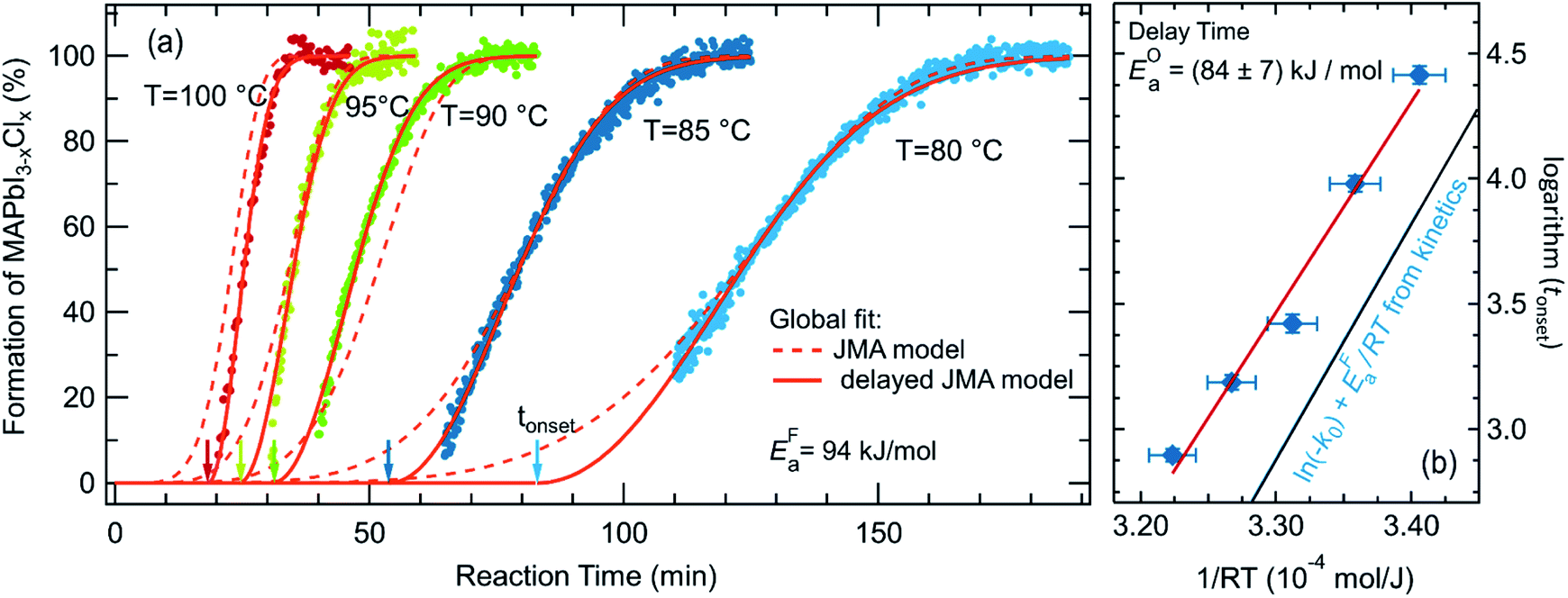 | ||
| Fig. 6 Kinetic data for the samples annealed at 80 °C, 85 °C, 90 °C, 95 °C and 100 °C. (a) showing the concentration of MAPbI3−xClx during formation together with the JMAK model fits with an assumed delay (solid lines) and without a delay (broken lines) (eqn (3)). (b) Arrhenius plot of the delay time tonset as determined by the global fit to the JMAK model to extract the activation energy of the delay process, resulting in EOa = 84 ± 7 kJ mol−1. As a comparison ln(kF0) + EFa/RT as obtained from the global fit of the formation kinetics for t > tonset is shown in blue. | ||
Kinetic parameters of the MAPbI3−xClx formation reaction can be extracted by applying an appropriate temperature-dependent formation model for the time evolution of the MAPbI3−xClx concentration c(t). The sigmoidal kinetics observed in Fig. 6a are characteristic for solid-state transformations and can be attributed to a nucleation and growth process. The widely used Johnson–Mehl–Avrami–Kolmogorov (JMAK) model57–59 describes such solid-state transformation reactions at constant temperature T and has been recently applied to the formation of perovskites from precursors.12 Model assumptions are that nucleation occurs homogenously distributed within the precursor phase, that the growth rate is constant in time and that growth occurs homogeneously in all directions.58 We apply the JMAK-model using a thermally activated rate equation that includes a delay time tonset to account for the observed delay in MAPbI3−xClx formation:
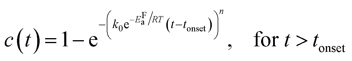 | (3) |
The dataset shown in Fig. 6a is fitted for all temperatures simultaneously, varying k0, EFa and n globally for all processes. Alternatively, tonset is fixed to zero for the pure JMAK model while it assumes temperature-dependent finite values for the altered model given by eqn (3). From fitting the data in Fig. 6, it can be seen, that if the delay time is omitted (tonset = 0 min) the global fit insufficiently describes the measured data and results in a growth dimensionality of n = 5.5, which is physically difficult to rationalize. When introducing a delay time tonset(T), the experimental data can be fitted with higher accuracy for all temperatures, which can be also seen from the χ2-coefficient which decreases from 11 to 6. The resulting activation energy of the formation reaction is EFa = (94 ± 2) kJ mol−1 and the growth exponent is n = 2.1 ± 0.1. The growth exponent corresponds to the dimensionality of the growth, where n = 2 implies 2-dimensional growth of previously nucleated material. As a growth exponent n > 4 bears no physical meaning, this shows that the formation of MAPbI3−xClx can only be correctly described by including a temporal delay in the onset of MAPbI3−xClx formation (eqn (3)).
In addition, a second activation energy can be extracted from the delay times. Fig. 6b shows an Arrhenius plot of the delay times tonset yielding an activation energy of EOa = (84 ± 7) kJ mol−1. Although both activation energies, estimated from the temperature dependence of tonset(T) and from the temperature dependence of the subsequent formation kinetics, are very close to each other we believe that they may correspond to two distinct phenomena, as discussed further below.12,60
A comparison of the reaction kinetics determined in the present study with previously reported reaction kinetics observed by in situ GIWAXS shows some agreement and some differences (Fig. S14 in ESI†). While Chang,40 Unger25 and Stone28 observe a delay, this is not observed by Moore et al.12 The reported duration for complete conversion of the precursor to the final film varies from 30 min to 70 min at 100 °C and the reported activation energies vary from 69 kJ mol−160 to 86 ± 6 kJ mol−1.12 It has to be noted, that these activation energies were obtained without including a formation delay. A comparison of the previously presented data shows that even though the formation onset differs significantly in different studies, the reaction kinetics after the formation onset obtained in the present study agree with the data presented by Chang, Unger and Stone25,28,40 and hence seem to be more fundamental than the delay time (see Fig. S14†). Thus, we propose that variations observed for the formation onset strongly depend on the processing conditions. The annealing environment, N2 or dry air, varying relative humidity or ambient temperature is often not specified in detail but may have a crucial influence. This variance in process conditions and kinetics serves as a strong argument for the relevance of in situ process control during growth.
The strong variation of tonset visible in the literature data and in this study for different glovebox temperatures (see ESI, Fig. S7b†), together with the largely unaffected subsequent formation kinetics, indicate that the processes occurring during the delay and the formation phase itself may be distinctively different.
Considering all data from PL, UV-Vis, XRD and XRF we conclude, that MACl and MA2PbClI3 as well as MAPbI3−xClx – nuclei coexist within the film from the beginning. The fact that the MAPbI3−xClx cannot be observed by XRD in the beginning of the growth process can be explained by an initially small-domain size of the crystallites. We recall from Fig. 1 and 4 that a photoluminescence signal is observed from t = 0 min which starts at a peak energy of 1.7 eV and then continuously red-shifts to 1.6 eV. Although such a continuous red shift may be explained by a growth of the MAPbI3−xClx nuclei and thus decreasing of quantum confinement, it may also be due to a continuous substitution of chlorine with iodine within the MAPbI3−xClx seed crystals. Assuming a linear dependence of the band-gap of MAPbI3−xClx on the chlorine content x, the PL peak energy would indicate a Cl-concentration of 6% of the original seed crystals at t = 0 min, subsequently reducing to about 0.6% for the fully annealed MAPbI3−xClx film. This explanation is consistent with the Rietveld refinement of the powder diffractograms which show an increase of the unit cell volume approaching MAPbI3 literature values for t > 40 min (see Fig. S2 in the ESI†), indicating a decrease of the Cl content in MAPbI3−xClx from that point onwards.43,61,62
MACl was shown to evaporate during the process25 which correlates to a loss of chlorine within the film, as measured with XRF (Fig. 4). Once MACl is fully evaporated, further evaporation of chlorine leads to a decomposition of the MA2PbClI3 precursor. By this, the limiting elements (Pb/I) become available and thus a sudden formation onset of MAPbI3−xClx can be observed. Thus, we propose an activation energy of EOa = (84 ± 7) kJ mol−1 for the loss of Cl in form of MACl during the latent phase and an activation energy EFa = (94 ± 2) kJ mol−1 for the subsequent formation of MAPbI3−xClx and decomposition of MA2PbClI3.
3. Conclusions
The evolution of halide perovskite formation was monitored in situ by optical spectroscopy during a regular solar cell synthesis process in a glovebox environment. The band-edge of the growing perovskite material was observed by white light reflection and fitted with an analytical model to extract the evolution of the MAPbI3 concentration in the thin film during annealing. Simultaneously, the optical properties of the film are monitored by photoluminescence which allows us to quantitatively deduce the implied Voc during film growth.Analyzing the MAI/PbCl2 based synthesis route it was found that a crystalline precursor phase develops which can be attributed to MA2PbClI3. Furthermore, the excess of chlorine is shown to delay the onset of MAPbI3−xClx formation. We propose that already from the beginning of the growth process MAPbI3−xClx nuclei exist, (with strong luminescence at 1.7 eV) from which the MAPbI3−xClx layer forms only after a delay time tonset. This is supported by a growth exponent of n = 2 for the formation of MAPbI3−xClx, indicating 2D growth with previous nucleation, and a PL emission which continuously approaches the final MAPbI3−xClx emission. By correlation with TRPL measurements we observed that the excited charge carrier lifetime stays nearly constant during annealing, however the effective doping density decreases significantly. This can be attributed to a loss of methylammoniumchloride during annealing. Thus, it is shown that through in situ monitoring the doping density could be fine-tuned by altering the annealing time. This work demonstrates the great potential of in situ optical spectroscopy in order to monitor and tailor the optoelectronic properties of hybrid perovskites directly during device processing. Furthermore, the possibility to analyze real growth processes in detail opens the way to an improved understanding and enhanced reproducibility of halide perovskite solution processing, which is a necessary prerequisite for up scaling approaches.
4. Experimental section
4.1 Perovskite synthesis
FTO coated glass substrates (Pilkington TEC7) were cleaned in an ultrasonic bath, using a laboratory cleaning agent (diluted Extran 1:1 with H2O) and subsequently rinsed with distilled water and dried with N2. The substrates were coated with a 75 nm thick layer of TiO2 by electron beam evaporation and annealed in ambient air at 500 °C for 2 h. To enable the reflection/transmission measurements the back side of the substrates was coated with 150 nm of silver by electron beam evaporation. Methylammonium iodide (MAI) was prepared from methylamine and HI as described elsewhere.10
Lead(II) chloride was used as purchased from Sigma Aldrich. MAI and lead chloride were dissolved in anhydrous N,N-dimethylformamide (DMF) in a 3:1 ratio10 and stirred for 30 min at 20 °C in a nitrogen-filled glovebox. 150 μl of the solution were drop cast onto the TiO2 coated substrate and spin coated at 2000 rpm for 45 s. After spin coating, the samples were first left to dry for 30 min at 20 °C (ref. 63) and afterwards annealed on a hotplate at 100 °C until the perovskite was fully formed.10
4.2 In situ monitoring
For the in situ photoluminescence a custom setup was used in which the samples are excited with a blue LED (455 nm) at an intensity of 3 mW cm−2 and the luminescence is detected with a fiber-coupled spectrometer with a spectral range of 341 to 1022 nm and spectral resolution of 0.28 nm. In situ reflectance measurements were performed in the same setup using a 20 W tungsten halogen lamp for excitation and the same fiber-coupled spectrometer for signal detection.During all room temperature measurements the temperature in the glovebox was kept constant at 20 ± 0.5 °C. The temperature of the samples was determined using a Pt100 resistor.
4.3 Ex situ characterization
X-ray diffraction measurements were performed with a Panalytical X'PERT-PRO diffractometer using Cu Kα-radiation. The samples were measured for 53 min between 2Θ = 10° and 70° in Bragg–Brentano geometry. All measured patterns were corrected for Cu Kα2-emission using the X'Pert Highscore Plus software tool.X-ray fluorescence was measured in a custom system (IFG) using a rhodium tube with a micro-focus capillary optics with a focus spot size of 100 μm. The fluorescence signal is detected with an energy dispersive detector with a resolution of 190 eV. For the measurements of the Cl-content a mean value and the standard deviation was calculated from 4 spots of each sample. The standard deviation of the Cl content lies between 0.1 and 0.2% and thus is smaller than the marker size in Fig. 4d.
Time-resolved photoluminescence was measured by excitation with a pulsed laser with 660 nm wavelength (pulse duration 100 ps) detection with a Si-Avalanche Photo Diode (time resolution 60 ps). Repetition rates of either 1 MHz or 250 kHz were used, depending on the transients measured. The excitation density, calculated from the time-averaged laser power, the repetition rate of the pulses, the spot size of the laser on the sample and absorption coefficient was Φ = 2.45 × 10¹⁵ photons per cm3 per pulse.
Conflicts of interest
There are no conflicts to declare.Acknowledgements
The authors gratefully acknowledge José Márquez Prieto and Steffen Kretzschmar and David Diering for support with optical alignment and calibrations, Martin Kärgell for synthesis of MAI and Lars Steinkopf for technical support. E. U. and K. S. acknowledge funding from the Swedish Research Council (Project 2015-00163 and Project 2018-05014) and Marie Sklodowska Curie Actions Cofund Project INCA (grant number 600398). P. B. and D. D. acknowledge support by the joint University Potsdam–HZB graduate school ‘hypercells’. E. U. acknowledges funding from the German Ministry of Education and Research (BMBF) for the Young Investigator Group Hybrid Materials Formation and Scaling (HyPerFORME) within the program “NanoMatFutur” (grant no. 03XP0091).References
- M. A. Green, E. D. Dunlop, J. Hohl-Ebinger, M. Yoshita, N. Kopidakis and A. W. Y. Ho-Baillie, Solar Cell Efficiency Tables (Version 55), Prog. Photovoltaics Res. Appl., 2020, 28(1), 3–15, DOI:10.1002/pip.3228.
- M. Saliba, T. Matsui, K. Domanski, J.-Y. Seo, A. Ummadisingu, S. M. Zakeeruddin, J.-P. Correa-Baena, W. R. Tress, A. Abate, A. Hagfeldt and M. Grätzel, Incorporation of Rubidium Cations into Perovskite Solar Cells Improves Photovoltaic Performance, Science, 2016, 354(6309), 206–209, DOI:10.1126/science.aah5557.
- M. Saliba, T. Matsui, J.-Y. Seo, K. Domanski, J.-P. Correa-Baena, K. N. Mohammad, S. M. Zakeeruddin, W. Tress, A. Abate, A. Hagfeldt and M. Grätzel, Cesium-Containing Triple Cation Perovskite Solar Cells: Improved Stability, Reproducibility and High Efficiency, Energy Environ. Sci., 2016, 9, 1989–1997, 10.1039/C5EE03874J.
- E. L. Unger, L. Kegelmann, K. Suchan, D. Sörell, L. Korte and S. Albrecht, Roadmap and Roadblocks for the Band Gap Tunability of Metal Halide Perovskites, J. Mater. Chem. A, 2017, 5(23), 11401–11409, 10.1039/C7TA00404D.
- W. A. Dunlap-Shohl, Y. Zhou, N. P. Padture and D. B. Mitzi, Synthetic Approaches for Halide Perovskite Thin Films, Chem. Rev., 2019, 119(5), 3193–3295 CrossRef CAS PubMed.
- V. L. Pool, B. Dou, D. G. Van Campen, T. R. Klein-Stockert, F. S. Barnes, S. E. Shaheen, M. I. Ahmad, M. F. A. M. van Hest and M. F. Toney, Thermal Engineering of FAPbI3 Perovskite Material via Radiative Thermal Annealing and In Situ XRD, Nat. Commun., 2017, 8, 14075, DOI:10.1038/ncomms14075.
- G. E. Eperon, V. M. Burlakov, P. Docampo, A. Goriely and H. Snaith, J. Morphological Control for High Performance, Solution-Processed Planar Heterojunction Perovskite Solar Cells, Adv. Funct. Mater., 2014, 24(1), 151–157, DOI:10.1002/adfm.201302090.
- N. J. Jeon, J. H. Noh, Y. C. Kim, W. S. Yang, S. Ryu and S. I. Seok, Solvent Engineering for High-Performance Inorganic-Organic Hybrid Perovskite Solar Cells, Nat. Mater., 2014, 13(9), 897–903, DOI:10.1038/nmat4014.
- N.-G. Park, Crystal Growth Engineering for High Efficiency Perovskite Solar Cells, CrystEngComm, 2016, 18(32), 5977–5985, 10.1039/C6CE00813E.
- M. M. Lee, J. Teuscher, T. Miyasaka, T. N. Murakami and H. J. Snaith, Efficient Hybrid Solar Cells Based on Meso-Superstructured Organometal Halide Perovskites, Science, 2012, 338(6107), 643–647, DOI:10.1126/science.1228604.
- A. Buin, P. Pietsch, J. Xu, O. Voznyy, A. H. Ip, R. Comin and E. H. Sargent, Materials Processing Routes to Trap-Free Halide Perovskites, Nano Lett., 2014, 14(11), 6281–6286, DOI:10.1021/nl502612m.
- D. T. Moore, H. Sai, K. W. Tan, D.-M. Smilgies, W. Zhang, H. J. Snaith, U. Wiesner and L. A. Estroff, Crystallization Kinetics of Organic–Inorganic Trihalide Perovskites and the Role of the Lead Anion in Crystal Growth, J. Am. Chem. Soc., 2015, 137(6), 2350–2358, DOI:10.1021/ja512117e.
- Z. Liu, L. Krückemeier, B. Krogmeier, B. Klingebiel, J. A. Márquez, S. Levcenko, S. Öz, S. Mathur, U. Rau, T. Unold and T. Kirchartz, Open-Circuit Voltages Exceeding 1.26 V in Planar Methylammonium Lead Iodide Perovskite Solar Cells, ACS Energy Lett., 2019, 4(1), 110–117, DOI:10.1021/acsenergylett.8b01906.
- N. K. Noel, S. N. Habisreutinger, B. Wenger, M. T. Klug, M. T. Hörantner, M. B. Johnston, R. J. Nicholas, D. T. Moore and H. J. Snaith, A Low Viscosity, Low Boiling Point, Clean Solvent System for the Rapid Crystallisation of Highly Specular Perovskite Films, Energy Environ. Sci., 2017, 10(1), 145–152, 10.1039/C6EE02373H.
- A. Barrows, A. Pearson, C. Kwak, A. Dunbar, A. Buckley and D. Lidzey, Efficient Planar Heterojunction Mixed-Halide Perovskite Solar Cells Deposited via Spray-Deposition, Energy Environ. Sci., 2014, 7(9), 2944–2950, 10.1039/C4EE01546K.
- Y. Deng, E. Peng, Y. Shao, Z. Xiao, Q. Dong and J. Huang, Scalable Fabrication of Efficient Organolead Trihalide Perovskite Solar Cells with Doctor-Bladed Active Layers, Energy Environ. Sci., 2015, 8(5), 1544–1550 RSC.
- F. Mathies, T. Abzieher, A. Hochstuhl, K. Glaser, A. Colsmann, U. W. Paetzold, G. Hernandez-Sosa, U. U. Lemmer, A. Quintilla, D. Rueda, A. Quintilla and U. U. Lemmer, Multipass Inkjet Printed Planar Methylammonium Lead Iodide Perovskite Solar Cells, J. Mater. Chem. A, 2016, 4, 994209, 10.1039/C6TA07972E.
- K. Hwang, Y.-S. Jung, Y.-J. Heo, F. H. Scholes, S. E. Watkins, J. Subbiah, D. J. Jones, D.-Y. Kim and D. Vak, Toward Large Scale Roll-to-Roll Production of Fully Printed Perovskite Solar Cells, Adv. Mater., 2015, 27(7), 1241–1247, DOI:10.1002/adma.201404598.
- T. M. Schmidt, T. T. Larsen-Olsen, J. E. Carlé, D. Angmo and F. C. Krebs, Upscaling of Perovskite Solar Cells: Fully Ambient Roll Processing of Flexible Perovskite Solar Cells with Printed Back Electrodes, Adv. Energy Mater., 2015, 5(15), 1500569, DOI:10.1002/aenm.201500569.
- M. Anaya, J. F. Galisteo-López, M. E. Calvo, C. López and H. Míguez, Photophysical Analysis of the Formation of Organic–Inorganic Trihalide Perovskite Films: Identification and Characterization of Crystal Nucleation and Growth, J. Phys. Chem. C, 2016, 120(5), 3071–3076, DOI:10.1021/acs.jpcc.6b00398.
- M. D. Heinemann, R. Mainz, F. Österle, H. Rodriguez-Alvarez, D. Greiner, C. A. Kaufmann and T. Unold, Evolution of Opto-Electronic Properties during Film Formation of Complex Semiconductors, Sci. Rep., 2017, 7(1), 1–9, DOI:10.1038/srep45463.
- J. Burschka, N. Pellet, S.-J. Moon, R. Humphry-Baker, P. Gao, M. K. Nazeeruddin and M. Grätzel, Sequential Deposition as a Route to High-Performance Perovskite-Sensitized Solar Cells, Nature, 2013, 499(7458), 316–319, DOI:10.1038/nature12340.
- J. J. v. Franeker, K. H. Hendriks, B. J. Bruijnaers, M. W. G. M. Verhoeven, M. M. Wienk and R. a. J. Janssen, Monitoring Thermal Annealing of Perovskite Solar Cells with in situ Photoluminescence, Adv. Energy Mater., 2017, 7(7), 1–9, DOI:10.1002/aenm.201601822.
- F. Babbe and C. M. Sutter-Fella, Optical Absorption-Based In Situ Characterization of Halide Perovskites, Adv. Energy Mater., 2020, 1903587, DOI:10.1002/aenm.201903587.
- E. L. Unger, A. R. Bowring, C. J. Tassone, V. L. Pool, A. Gold-Parker, R. Cheacharoen, K. H. Stone, E. T. Hoke, M. F. Toney and M. D. McGehee, Chloride in Lead Chloride-Derived Organo-Metal Halides for Perovskite-Absorber Solar Cells, Chem. Mater., 2014, 26(24), 7158–7165, DOI:10.1021/cm503828b.
- Z. Song, S. C. Watthage, A. B. Phillips, B. L. Tompkins, R. J. Ellingson and M. J. Heben, Impact of Processing Temperature and Composition on the Formation of Methylammonium Lead Iodide Perovskites, Chem. Mater., 2015, 27(13), 4612–4619, DOI:10.1021/acs.chemmater.5b01017.
- M. Saliba, K. W. Tan, H. Sai, D. T. Moore, T. Scott, W. Zhang, L. A. Estroff, U. Wiesner and H. J. Snaith, The Influence of Thermal Processing Protocol upon the Crystallization and Photovoltaic Performance of Organic-Inorganic Lead Trihalide Perovskites, J. Phys. Chem. C, 2014, 118(30), 17171–17177, DOI:10.1021/jp500717w.
- K. H. Stone, A. Gold-Parker, V. L. Pool, E. L. Unger, A. R. Bowring, M. D. McGehee, M. F. Toney and C. J. Tassone, Transformation from Crystalline Precursor to Perovskite in PbCl2-Derived MAPbI3, Nat. Commun., 2018, 9(1), 3458, DOI:10.1038/s41467-018-05937-4.
- A. Binek, I. Grill, N. Huber, K. Peters, A. G. Hufnagel, M. Handloser, P. Docampo, A. Hartschuh and T. Bein, Control of Perovskite Crystal Growth by Methylammonium Lead Chloride Templating, Chem.–Asian J., 2016, 11(8), 1199–1204, DOI:10.1002/asia.201501379.
- A. Dualeh, N. Tétreault, T. Moehl, P. Gao, M. K. Nazeeruddin and M. Grätzel, Effect of Annealing Temperature on Film Morphology of Organic-Inorganic Hybrid Pervoskite Solid-State Solar Cells, Adv. Funct. Mater., 2014, 24(21), 3250–3258, DOI:10.1002/adfm.201304022.
- S. D. Stranks, G. E. Eperon, G. Grancini, C. Menelaou, M. J. P. Alcocer, T. Leijtens, L. M. Herz, A. Petrozza and H. J. Snaith, Electron-Hole Diffusion Lengths Exceeding 1 Micrometer in an Organometal Trihalide Perovskite Absorber, Science, 2013, 342(6156), 341–344, DOI:10.1126/science.1243982.
- S. T. Williams, F. Zuo, C.-C. Chueh, C.-Y. Liao, P.-W. Liang and A. K.-Y. Jen, Role of Chloride in the Morphological Evolution of Organo-Lead Halide Perovskite Thin Films, ACS Nano, 2014, 8(8), 10640–10654 CrossRef CAS PubMed.
- C. Wehrenfennig, G. E. Eperon, M. B. Johnston, H. J. Snaith and L. M. Herz, High Charge Carrier Mobilities and Lifetimes in Organolead Trihalide Perovskites, Adv. Mater., 2014, 26(10), 1584–1589, DOI:10.1002/adma.201305172.
- D. W. d. Quilettes, S. M. Vorpahl, S. D. Stranks, H. Nagaoka, G. E. Eperon, M. E. Ziffer, H. J. Snaith and D. S. Ginger, Impact of Microstructure on Local Carrier Lifetime in Perovskite Solar Cells, Science, 2015, 348(6235), 683–686, DOI:10.1126/science.aaa5333.
- E. L. Unger, T. Edvinsson, J. D. Roy-Mayhew, H. Rensmo, A. Hagfeldt, E. M. J. Johansson and G. Boschloo, Excitation Energy Dependent Charge Separation at Hole-Transporting Dye/TiO2 Hetero Interface, J. Phys. Chem. C, 2012, 116(40), 21148–21156, DOI:10.1021/jp302187w.
- V. L. Pool, A. Gold-Parker, M. D. McGehee and M. F. Toney, Chlorine in PbCl2-Derived Hybrid-Perovskite Solar Absorbers, Chem. Mater., 2015, 27(25), 7240–7243 CrossRef CAS.
- D. E. Starr, G. Sadoughi, E. Handick, R. G. Wilks, J. H. Alsmeier, L. Kö, M. Gorgoi, H. J. Snaith and M. Bä, Direct Observation of an Inhomogeneous Chlorine Distribution in CH3NH3PbI3ÀxClx Layers: Surface Depletion and Interface Enrichment, Energy Environ. Sci., 2015, 8(8), 1609–1615, 10.1039/c5ee00403a.
- H. Yu, F. Wang, F. Xie, W. Li, J. Chen and N. Zhao, The Role of Chlorine in the Formation Process of “CH3NH3PbI3−xClx” Perovskite, Adv. Funct. Mater., 2014, 24(45), 7102–7108 CAS.
- D. T. Moore, H. Sai, K. Wee Tan, L. A. Estroff and U. Wiesner, Impact of the Organic Halide Salt on Final Perovskite Composition for Photovoltaic Applications, APL Mater., 2014, 2(8), 081802, DOI:10.1063/1.4886275.
- C.-Y. Chang, Y.-C. Huang, C.-S. Tsao and W.-F. Su, Formation Mechanism and Control of Perovskite Films from Solution to Crystalline Phase Studied by In Situ Synchrotron Scattering, ACS Appl. Mater. Interfaces, 2016, 8(40), 26712–26721, DOI:10.1021/acsami.6b07468.
- A. T. Barrows, S. Lilliu, A. J. Pearson, D. Babonneau, A. D. F. Dunbar and D. G. Lidzey, Monitoring the Formation of a CH3NH3PbI3−XClx Perovskite during Thermal Annealing Using X-Ray Scattering, Adv. Funct. Mater., 2016, 26(27), 4934–4942, DOI:10.1002/adfm.201601309.
- M. Alsari, O. Bikondoa, J. Bishop, M. Abdi-Jalebi, L. Y. Ozer, M. Hampton, P. Thompson, M. T. Hörantner, S. Mahesh, C. Greenland, J. E. Macdonald, G. Palmisano, H. J. Snaith, D. G. Lidzey, S. D. Stranks, R. H. Friend and S. Lilliu, In Situ Simultaneous Photovoltaic and Structural Evolution of Perovskite Solar Cells during Film Formation, Energy Environ. Sci., 2018, 11(2), 383–393, 10.1039/C7EE03013D.
- T. Baikie, N. S. Barrow, Y. Fang, P. J. Keenan, P. R. Slater, R. O. Piltz, M. Gutmann, S. G. Mhaisalkar and T. J. White, A Combined Single Crystal Neutron/X-Ray Diffraction and Solid-State Nuclear Magnetic Resonance Study of the Hybrid Perovskites CH3NH3PbX3 (X = I, Br and Cl), J. Mater. Chem. A, 2015, 3(17), 9298–9307, 10.1039/C5TA01125F.
- E. Edri, S. Kirmayer, M. Kulbak, G. Hodes and D. Cahen, Chloride Inclusion and Hole Transport Material Doping to Improve Methyl Ammonium Lead Bromide Perovskite-Based High Open-Circuit Voltage Solar Cells, J. Phys. Chem. Lett., 2014, 5(3), 429–433, DOI:10.1021/jz402706q.
- S. Colella, E. Mosconi, G. Pellegrino, A. Alberti, V. L. P. Guerra, S. Masi, A. Listorti, A. Rizzo, G. G. Condorelli, F. D. Angelis and G. Gigli, Elusive Presence of Chloride in Mixed Halide Perovskite Solar Cells, J. Phys. Chem. Lett., 2014, 5(20), 3532–3538 CrossRef CAS PubMed.
- T. Kirchartz and U. Rau, Electroluminescence Analysis of High Efficiency Cu(In,Ga)Se2 Solar Cells, J. Appl. Phys., 2007, 102(10), 104510, DOI:10.1063/1.2817959.
- T. Dittrich, C. Awino, P. Prajongtat, B. Rech and M. C. Lux-Steiner, Temperature Dependence of the Band Gap of CH3NH3PbI3 Stabilized with PMMA: A Modulated Surface Photovoltage Study, J. Phys. Chem. C, 2015, 119(42), 23968–23972, DOI:10.1021/acs.jpcc.5b07132.
- M. A. Green, Y. Jiang, A. M. Soufiani and A. Ho-Baillie, Optical Properties of Photovoltaic Organic–Inorganic Lead Halide Perovskites, J. Phys. Chem. Lett., 2015, 6(23), 4774–4785, DOI:10.1021/acs.jpclett.5b01865.
- M. Stolterfoht, C. M. Wolff, J. A. Márquez, S. Zhang, C. J. Hages, D. Rothhardt, S. Albrecht, P. L. Burn, P. Meredith, T. Unold and D. Neher, Visualization and Suppression of Interfacial Recombination for High-Efficiency Large-Area Pin Perovskite Solar Cells, Nat. Energy, 2018, 3(10), 847–854, DOI:10.1038/s41560-018-0219-8.
- R. T. Ross, Some Thermodynamics of Photochemical Systems, J. Chem. Phys., 1967, 46(12), 4590–4593, DOI:10.1063/1.1840606.
- S. Rühle, Tabulated Values of the Shockley–Queisser Limit for Single Junction Solar Cells, Sol. Energy, 2016, 130, 139–147, DOI:10.1016/j.solener.2016.02.015.
- R. K. Ahrenkiel, Minority-Carrier Lifetime in III–V Semiconductors, in Semiconductors and Semimetals, ed. R. K. Ahrenkiel and M. S. Lundstrom, Elsevier, 1993, vol. 39, ch. 2, pp. 39–150, DOI:10.1016/S0080-8784(08)62594-6.
- T. Unold and L. Gütay, Photoluminescence Analysis of Thin-Film Solar Cells, in Advanced Characterization Techniques for Thin Film Solar Cells, ed. D. Abou-Ras, T. Kirchartz and U. Rau, Wiley-VCH Verlag GmbH & Co. KGaA, Weinheim, Germany, 2011, pp. 151–175, DOI:10.1002/9783527636280.ch7.
- A. Redinger, S. Levcenko, C. J. Hages, D. Greiner, C. A. Kaufmann and T. Unold, Time Resolved Photoluminescence on Cu(In,Ga)Se2 Absorbers: Distinguishing Degradation and Trap States, Appl. Phys. Lett., 2017, 110(12), 122104, DOI:10.1063/1.4977707.
- Q. Wang, Y. Shao, H. Xie, L. Lyu, X. Liu, Y. Gao and J. Huang, Qualifying Composition Dependent p and n Self-Doping in CH3NH3PbI3, Appl. Phys. Lett., 2014, 105(16), 163508, DOI:10.1063/1.4899051.
- W.-J. Yin, T. Shi and Y. Yan, Unusual Defect Physics in CH3NH3PbI3 Perovskite Solar Cell Absorber, Appl. Phys. Lett., 2014, 104(6), 063903, DOI:10.1063/1.4864778.
- M. Avrami, Kinetics of Phase Change. II Transformation-Time Relations for Random Distribution of Nuclei, J. Chem. Phys., 1940, 8(2), 212–224, DOI:10.1063/1.1750631.
- M. Avrami, Kinetics of Phase Change. I General Theory, J. Chem. Phys., 1939, 7(12), 1103–1112, DOI:10.1063/1.1750380.
- M. Avrami, Granulation, Phase Change, and Microstructure Kinetics of Phase Change. III, J. Chem. Phys., 1941, 9(2), 177–184, DOI:10.1063/1.1750872.
- B. Wang, K. Young Wong, X. Xiao and T. Chen, Elucidating the Reaction Pathways in the Synthesis of Organolead Trihalide Perovskite for High-Performance Solar Cells, Sci. Rep., 2015, 5, 10557, DOI:10.1038/srep10557.
- A. Poglitsch and D. Weber, Dynamic Disorder in Methylammoniumtrihalogenoplumbates(II) Observed by Millimeter-wave Spectroscopy, J. Chem. Phys., 1987, 87(11), 6373–6378, DOI:10.1063/1.453467.
- T. Baikie, Y. Fang, J. M. Kadro, M. Schreyer, F. Wei, S. G. Mhaisalkar, M. Graetzel and T. J. White, Synthesis and Crystal Chemistry of the Hybrid Perovskite (CH3NH3)PbI3 for Solid-State Sensitised Solar Cell Applications, J. Mater. Chem. A, 2013, 1(18), 5628–5641, 10.1039/C3TA10518K.
- M.-F. Xu, H. Zhang, S. Zhang, H. L. Zhu, H.-M. Su, J. Liu, K. S. Wong, L.-S. Liao and W. C. H. Choy, A Low Temperature Gradual Annealing Scheme for Achieving High Performance Perovskite Solar Cells with No Hysteresis, J. Mater. Chem. A, 2015, 3(27), 14424–14430, 10.1039/C5TA02730F.
Footnote |
| † Electronic supplementary information (ESI) available. See DOI: 10.1039/d0ta01237h |
| This journal is © The Royal Society of Chemistry 2020 |