
A pulse electrodeposited amorphous tunnel layer stabilises Cu2O for efficient photoelectrochemical water splitting under visible-light irradiation†
Hao
Wu
ab,
Zhaoke
Zheng
c,
Cui Ying
Toe
 b,
Xiaoming
Wen
d,
Judy N.
Hart
e,
Rose
Amal
b and
Yun Hau
Ng
*ab
b,
Xiaoming
Wen
d,
Judy N.
Hart
e,
Rose
Amal
b and
Yun Hau
Ng
*ab
aSchool of Energy and Environment, City University of Hong Kong, Kowloon, Hong Kong, SAR, P. R. China. E-mail: yunhau.ng@cityu.edu.hk
bParticles and Catalysis Research Group, School of Chemical Engineering, UNSW, Sydney, NSW 2052, Australia
cState Key Laboratory of Crystal Materials, Shandong University, Jinan 250100, China
dCentre for Micro-Photonics, Swinburne University of Technology, Hawthorn, VIC 3122, Australia
eSchool of Materials Science and Engineering, UNSW, Sydney, NSW 2052, Australia
First published on 10th February 2020
Abstract
Surface coating of a protective layer can prevent the corrosion of Cu2O at electrode liquid junctions (ELJs) in photoelectrochemical water splitting. However, a facile methodology for the deposition of a conformal protective layer is still a challenge. Here, an ultrathin layer of amorphous ZnO is introduced on Cu2O by pulsed electrodeposition, to construct a “sandwich” structure of a composite photoelectrode of TiO2/ZnO/Cu2O on an FTO substrate. Time-of-flight secondary ion mass spectrometry (ToF-SIMS) visualises the spatial distribution of Ti, Zn, Cu, and Sn elements of the composite. Benefiting from the homogeneous coating of a ZnO layer, visible cracks in TiO2 coating are significantly reduced, thus preventing the direct contact between the electrolyte and Cu2O. Moreover, due to the ultrathin property of the amorphous ZnO layer, the energetic electrons from the excited Cu2O can be injected via the ZnO layer into TiO2, as elucidated by time-resolved photoluminescence (TRPL) results. The resulting composite photoelectrode shows enhanced photoelectrochemical activity and stability, compared to the bare Cu2O, as well as the TiO2/Cu2O photoelectrode. This study offers a versatile and effective method for improving the stability and charge separation efficiency of Cu2O, which is useful in guiding the surface coating of other nanostructured materials for solar energy conversion.
Introduction
Photoelectrochemical cells are a promising technology for mimicking artificial photosynthesis to generate solar fuel. The challenge of constructing an efficient photoelectrochemical system lies in the design of cost-effective and stable photoelectrode materials.1 Cu2O semiconductors have garnered extensive interest for various applications such as water splitting,2 CO2 reduction,3 and organic degradation.4 Nonetheless, the practical application of Cu2O is limited by its self-corrosion at electrode liquid junctions (ELJs).5–7 Paracchino et al. reported that the photoinduced electrons generated in Cu2O could corrode the Cu2O into Cu particles, rather than participate in reducing electron acceptors on the surface.8 Hence, developing strategies to prevent Cu2O from corroding at the ELJ is imperative to explore the full potential of Cu2O in photoelectrochemical applications.Introducing a protective layer on Cu2O is one of the most promising methods,9–16 which has attracted tremendous research interest. Carbon,9,17 NiOx,11,12 CuO,13,14 rGO,18,19 WO3,20 CoP,21 SnO2,22 and TiO2,23–28 have been reported as protective layers to suppress the corrosion of Cu2O. Of particular interest is the use of an atomic layer deposited (ALD) TiO2 layer, which has successfully been used in protecting various unstable materials such as p-InP,29 p-GaInP2,30 p-CIGS,31 p-Cu2ZnSnS4,32 p-P3HT/PCBM,33 and n-Si.34 However, given the non-uniform coating characteristic inherent to TiO2 grown on Cu2O,35,36 a chemical buffer layer between TiO2 and Cu2O is indispensable to affording the chemical stability. Thereby, Grätzel's group developed an ALD deposited buffer layer of Al-doped ZnO on a Cu2O photoelectrode, which exhibited highly active and stable photoelectrochemical performance.8 Inspired by his work, Delaunay et al. achieved a stable photocurrent for Cu2O by introducing an ALD deposited Ga2O3 buffer layer.25 These intermediate layers with ultrathin thickness and close contact provide more uniform hydroxylated surfaces for TiO2 to grow on, while also improving the charge separation efficiency of Cu2O under simulated sunlight irradiation.34,37
Atomic layer deposition is, however, too complicated and expensive for large-scale applications. It also requires that the precursor has reasonably high vapour pressure and good thermal stability, rendering some materials difficult or maybe even impossible for ALD use.34 Electrochemical synthesis is a simple and durable technique, which has already been applied for industrial purposes such as the protection of warship bodies.38 Moreover, various materials such as metal alloys, metal oxides, and metal chalcogenides can be obtained by electrochemical synthesis, depositing on conducting substrates to form photoelectrodes for photoelectrochemical applications.39–41
Electrodeposited metal oxide films are usually prepared by the single-step electrolysis of a solution containing metal ions, a process that is difficult to precisely control due to the fast nucleation rate in aqueous solution. Moreover, the nucleation of metal oxides usually requires a high bias potential which will inevitably corrode the Cu2O surface. Hence, the homogenous coating of a metal oxide layer on the Cu2O surface by single-step electrodeposition is challenging. Recently, our group has demonstrated pulsed electrodeposition as a more advanced technology that can achieve an outstanding level of control of the deposited thin films, including control of morphology, thickness, and distribution over nanostructured substrates.42–44 In a typical pulsed electrodeposition process, the deposition potential and current can be fixed as constants or tuned over time and applied at various intervals; therefore, it not only provides invaluably fine control over the growth process of protective layers but also avoids the corrosion of Cu2O at a continuous high bias potential. By exploiting pulsed electrodeposition, we demonstrate herein that the thinness and the uniform coverage of ZnO amorphous layers can be effectively controlled. Due to the ultrathin nature of the amorphous ZnO and TiO2 layers, time-of-flight secondary ion mass spectrometry (TOF-SIMS) and X-ray photoelectron spectroscopy (XPS) are utilised to characterise the multi-layered structure. Moreover, the deposited ZnO amorphous layer with an ultrathin thickness (<2.5 nm) improves the protection by TiO2 and expedites electron transfer from Cu2O to the electrolyte under visible-light irradiation. Time-resolved photoluminescence (TRPL) verifies the improved charge separation in the composite photoelectrodes. As a result, the integrated Cu2O photoelectrode achieves higher and more stable performance in the photoelectrochemical cell.
Experimental section
Electrodeposition of Cu2O
Cu2O thin films were deposited by an electrodeposition method as previously reported.45 Fluorine-doped tin oxide (FTO) conductive glass was sequentially cleaned in an ultrasonic bath of 50% ethanol/50% acetone and Milli-Q water for 10 min. Then, Cu2O was electrodeposited onto the pre-cleaned FTO substrate in a three-electrode cell with FTO, Pt foil, and an Ag/AgCl (1 M KCl) electrode as the working, counter and reference electrodes, respectively. The electrolyte was a mixture of 0.4 M copper sulphate and 1.0 M trisodium citrate with a pH of 12.5 adjusted by the addition of 2 M sodium hydroxide. A constant bias of −0.6 V vs. Ag/AgCl (1 M KCl) was supplied by a potentiostat (Metrohm Autolab PGSTAT M101) for 20 min at 60 °C.Synthesis of the ZnO buffer layer and TiO2 protection layer
Pulsed electrodeposition of ultrathin ZnO buffer layers was conducted in a similar cell as mentioned above. The electrolyte contained 0.1 M zinc nitrate and 0.2 M potassium nitrate. Then, the pH of the solution was adjusted to 6.0 by adding 0.1 M potassium hydroxide. The as-synthesised Cu2O/FTO electrode was applied as the working electrode. In contrast to single-step electrodeposition, pulsed electrodeposition was carried out by alternating the potentials between seeding (−1.1 V, 1 s) and nucleation (−0.75 V, 9 s) for 36, 48, and 60 pulses. The temperature was maintained at 70 °C through the whole process. TiO2 protecting layers were coated onto both the bare Cu2O and the ZnO/Cu2O electrodes by a dip-coating method. The process was conducted in a 0.1 M titanium isopropoxide ethanol solution for 30 min. Then, the electrode was subjected to mild heat treatment for 30 min in air to improve the chemical stability of the protective coatings. The treatment temperature was increased from room temperature to 180 °C with a ramping rate of 2.5 °C min−1 in a tube furnace and cooled down with a cooling rate of 2 °C min−1 to room temperature.Photoelectrochemical measurements
The photoelectrochemical performance of the Cu2O-based photoelectrodes was tested in a three-electrode configuration with the Cu2O-based working electrodes, an Ag/AgCl (1 M KCl) reference electrode and a Pt wire counter electrode. The electrolyte was 0.1 M Na2SO4 (pH 6.8) which was purged with N2 gas for 30 min before the measurements. Both photocurrent–potential (J–V) and photocurrent–time (J–t) curves were recorded under a chopped light from the front-side by using a 300 W xenon lamp equipped with a long-pass filter (>420 nm). The intensity of the light source was calibrated to be 200 mW cm−2 by uisng a Newport optical power meter. Linear sweep voltammetry was performed from 0 V to −0.6 V vs. Ag/AgCl (1 M KCl) at a scan rate of 2 mV s−1. Photoelectrochemical stability was investigated by time-based photocurrent measurements at a constant applied potential of −0.2 V vs. Ag/AgCl (1 M KCl).Faraday efficiency measurements were performed by side illumination of a gas-tight H-cell reactor through a quartz window. Platinum (Pt) nanoparticles were deposited on the prepared photoelectrode surface by an electrodeposition method. A bias of −0.1 V vs. Ag/AgCl (1 M KCl) was applied to the working electrode for 2 min in 1 mM H2PtCl6 aqueous solution. The illuminated area of the thin film was 1 cm2. The reaction chamber was purged with argon gas (50 mL min−1) for 30 min to remove air. The gas production reactions were conducted under illumination with a 300 W xenon lamp equipped with a long-pass filter (>420 nm). The evolved hydrogen was monitored by gas chromatography (Shimadzu GC-8A, HayeSep DB column).
Thin film characterisation
The crystalline structure of the Cu2O-based photoelectrodes was investigated by X-ray diffraction (PANalytical Empyrean) with Cu Kα radiation (1.54060 Å). The morphology was studied by field emission SEM (NanoSEM 450, FEI Nova). XPS data were collected using a Thermo Scientific (ESCALAB220i-XL) instrument with a monochromatic Al Kα X-ray source at 1486.68 eV. All XPS data were calibrated by the carbon 1s peak at 284.8 eV. The depth profile and 3D elemental distribution were analysed by using a time-of-flight secondary ion mass spectrometer (TOF-SIMS5, ION-TOF GmbH). Sputtering of the surface by using a 1 keV argon beam was carried out with an analysis area of 300 × 300 μm2. The etching rate was approximately 8 nm min−1. The optical absorption properties of the electrodes were determined by using a UV/Vis/NIR spectrophotometer (UV-3600, Shimadzu). The band gaps were calculated from the diffuse reflection spectra (DRS) according to the Kubelka–Munk theory. The fluorescence lifetime was measured by a time-correlated single-photon counting (TCSPC) technique on a Microtime-200 system (Picoquant) with excitation by using a 405 nm laser.Results and discussion
The synthesis flowchart of the TiO2/Cu2O and TiO2/ZnO/Cu2O photoelectrodes is illustrated in Scheme 1. A Cu2O thin film was first electrodeposited on the FTO substrate.45 Then, the ZnO layer was coated on Cu2O by pulsed electrodeposition. Several key parameters, such as pH of the electrolyte, applied potentials (for both the nucleation and growth stages), and time intervals, were carefully chosen to achieve homogenous coating without corroding Cu2O. In a typical pulsing cycle, Zn-based nuclei were quickly formed on the Cu2O at a potential of −1.1 V vs. Ag/AgCl (1 M KCl) for 1 s. The potential was then tuned to −0.75 V for 9 s to allow the subsequent growth of the as-deposited nuclei. The square-wave pulsing mode was repeated for 36, 48, and 60 cycles to control the coverage and thickness of the ZnO layer. In the final stage, the as-prepared ZnO/Cu2O and Cu2O photoelectrodes were dip-coated in a sol–gel containing 0.1 M tetraisopropoxide ethanol solution (TiO2 precursor) to deposit TiO2 protective layers.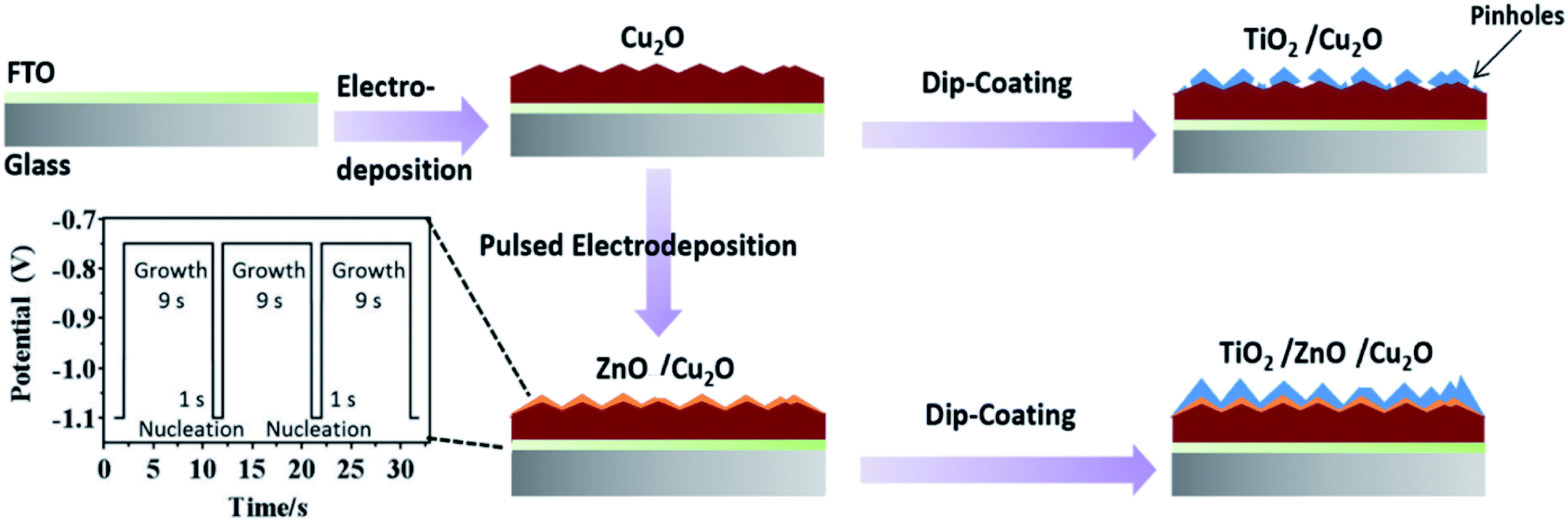 | ||
| Scheme 1 Flowchart of the synthesis process for TiO2/Cu2O and TiO2/ZnO/Cu2O multilayered photoelectrodes. | ||
Characterisation of the photoelectrodes
According to the scanning electron microscope (SEM) top-view images of Cu2O (Fig. 1a and S2a†), a compact Cu2O thin film with an average crystal size of 500 nm was deposited on FTO glass. The formed cubic morphology can be ascribed to the high stability of the {100} planes of Cu2O.46,47 When the pulsed electrodeposition process of ZnO was at 36 cycles, the formed layer showed an incomplete coverage with exposed surfaces of Cu2O (Fig. S1a†). After pulsed electrodeposition of ZnO for 48 cycles, the smooth surface of Cu2O is coated with an ultrathin and conformal layer (Fig. 1b). Thick layers with irregularly scattered dark spots were observed on Cu2O when the deposition was further increased to 60 cycles (Fig. S1b†), which is likely caused by the poor conductivity with increased thickness of amorphous materials under SEM.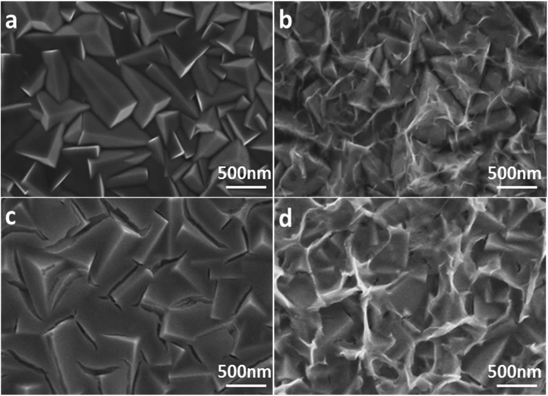 | ||
| Fig. 1 Top-view SEM images of (a) bare Cu2O, (b) ZnO/Cu2O, (c) TiO2/Cu2O, and (d) TiO2/ZnO/Cu2O photoelectrodes. | ||
Moreover, as proof of the significance of pulsed electrodeposition (as compared to the single-step deposition process), ZnO layers were also electrodeposited at constant potentials of −0.75 V and −1.1 V, respectively. Due to the insufficient electrical power at −0.75 V for the nucleation of ZnO, limited crystals were observed on Cu2O (Fig. S1c†). In contrast, when a continuous bias of −1.1 V was applied, stacked layers were scattered on the Cu2O surface with an increased thickness compared with that of the layers applied by the pulsed electrodeposition (Fig. S1d†). Notice that the colour of the Cu2O sample after the single-step electrodeposition at −1.1 V changed from reddish to dark black, indicating the corrosion of Cu2O. Based on these findings, pulsed electrodeposition with potentials supplied alternatively for nucleation and growth has proved to be critical to forming homogeneous ZnO layers with a controllable thickness without corroding Cu2O. As the conformal coating is indispensable to the protection of Cu2O, the ZnO/Cu2O layer synthesised by pulsed electrodeposition for 48 cycles was used for the following TiO2 coating.
After coating with TiO2 by a sol–gel method, the TiO2 that was directly coated on Cu2O showed many visible cracks (Fig. 1c), which was also observed in a very recent report.36 The report stated that the remediation of visible cracks in the TiO2 layer on the Cu2O surface is very challenging. However, the TiO2 coating with a ZnO underlayer, as designed in the present work, is homogenous and conformal across the entire irregular surface of Cu2O (Fig. 1d and S2b†). Note that the reduced cracks in the TiO2 layer are not likely to be filled by the pre-formed ZnO layer, which will be discussed in the post-reaction SEM study. The significant reduction in cracking can be attributed to the pre-formed ZnO layer, which functions as a chemical buffer (hydroxylated surfaces) to support the homogeneous growth of TiO2 on Cu2O. Achieving such a conformal protection layer is critical to the stable performance of Cu2O photoelectrodes.
SEM imaging and energy-dispersive spectroscopy (EDS) line-scan analysis were further conducted across a cross-section of the bare Cu2O and the TiO2/ZnO/Cu2O photoelectrodes. As shown in Fig. 2a, the Cu2O thin films deposited on FTO substrates have an average thickness of 500 nm deposited on the FTO substrate. The line-scan profile of bare Cu2O (Fig. 2b) indicates that the top and bottom layers contain Cu (Cu2O) and Sn (FTO), respectively. After coating with ZnO and TiO2, conformal coatings with an increased roughness compared with Cu2O were observed from the cross-section image (Fig. 2c), which is in agreement with the top-view SEM images. Moreover, obvious signals of Zn and Ti are observed on top of the Cu layer in the corresponding line-scan profiles (Fig. 2d), which suggests that ZnO and TiO2 make up the top layers above Cu2O. Note that there is an overlap of Ti and Zn signals between Cu2O and FTO, which is due to the irregular surfaces of the formed Cu2O. The crystalline phases of the photoelectrodes were characterised by X-ray diffraction (XRD). Since the Cu2O thin films were deposited onto FTO substrates, both the Cu2O and TiO2/ZnO/Cu2O photoelectrodes showed strong diffraction peaks assigned to Cu2O and FTO (Fig. S3†). In particular, the strongest diffraction peak at 36.4° is indexed to the (111) plane of cubic Cu2O (JCPDS 007-9767). No peaks of ZnO and TiO2 can be found in the XRD patterns, indicating that the ultrathin layers formed on Cu2O are likely to be amorphous.
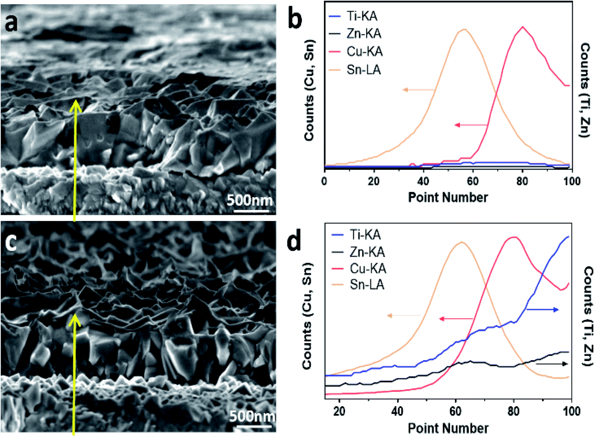 | ||
| Fig. 2 Cross-section SEM images and corresponding line-scan profiles of (a and b) bare Cu2O and (c and d) TiO2/ZnO/Cu2O photoelectrodes. The yellow arrow shows the scanning direction and the localised area where the SEM-EDS line-scan profiles were taken. | ||
To examine the “sandwich” structure of TiO2/ZnO/Cu2O and further define the chemical compositions of the coated amorphous layers, the prepared TiO2/ZnO/Cu2O photoelectrode was characterised by time-of-flight secondary ion mass spectrometry (ToF-SIMS) and X-ray photoelectron spectroscopy (XPS). ToF-SIMS is an advanced surface analysis technique that analyses secondary ions ejected by sputtering a focused primary ion beam on a surface. It has a very high surface-specific sensitivity, resulting in its use in detecting the penetration of ions in solid surfaces.48Fig. 3a shows the 3D rendered images of the TiO2/ZnO/Cu2O photoelectrode. From top to bottom, the electrode consists of four elemental layers, which are Ti, Zn, Cu, and Sn. This is further supported by the XPS depth profiles (Fig. 3b), which showed that the intensity of the Zn2+ signal increased and peaked at 250 s of Ar+ sputtering (region I), corresponding to a depth of approximately 30 nm below the Ti4+ top surface. The thickness of the ZnO layer was estimated to be smaller than 2.5 nm by correlating it with the etching speed. Note that the intensity of the Zn2+ signal is increased by six times, in Fig. 3b, due to its low intrinsic intensity. With further increase in sputtering time, the Ti4+ and Zn2+ signals declined drastically and disappeared with the emergence of the Cu+ signal (region II), indicating that the Ti4+ and Zn2+ layers are overlaid on top of Cu2O. There is an area of co-existence of Ti4+, Zn2+ and Cu+ shown in the depth profile (region II), which is caused by the irregular crystal surface of Cu2O. In region III, the signal intensity of Cu+ gradually decreased to 0% and the signal of Sn4+ emerges, indicating that the depth profile has reached the FTO substrate. The core-level XPS spectra of Zn 2p (Fig. 3c) for a ZnO/Cu2O photoelectrode show two peaks centered at binding energies of 1046.1 eV and 1023.1 eV, which are ascribed to the Zn 2p1/2 and Zn 2p3/2 spin–orbitals in the ZnO layer, respectively. After the deconvolution of the Zn 2p spectra, the peak-fitting results suggest that the predominant phase is ZnO with a small amount of Zn(OH)2. As shown in Fig. 3d, the core-level XPS spectrum of Ti 2p for the TiO2/ZnO/Cu2O photoelectrode shows two peaks at 465.2 eV and 459.5 eV which can be indexed to Ti 2p1/2 and Ti 2p3/2, indicating the successful deposition of TiO2. The foregoing results collectively suggest that the Cu2O thin film is conformally coated by an ultrathin layer of ZnO along with an upper amorphous layer of TiO2, thus enabling photoelectrochemical studies to understand the protection of these layers.
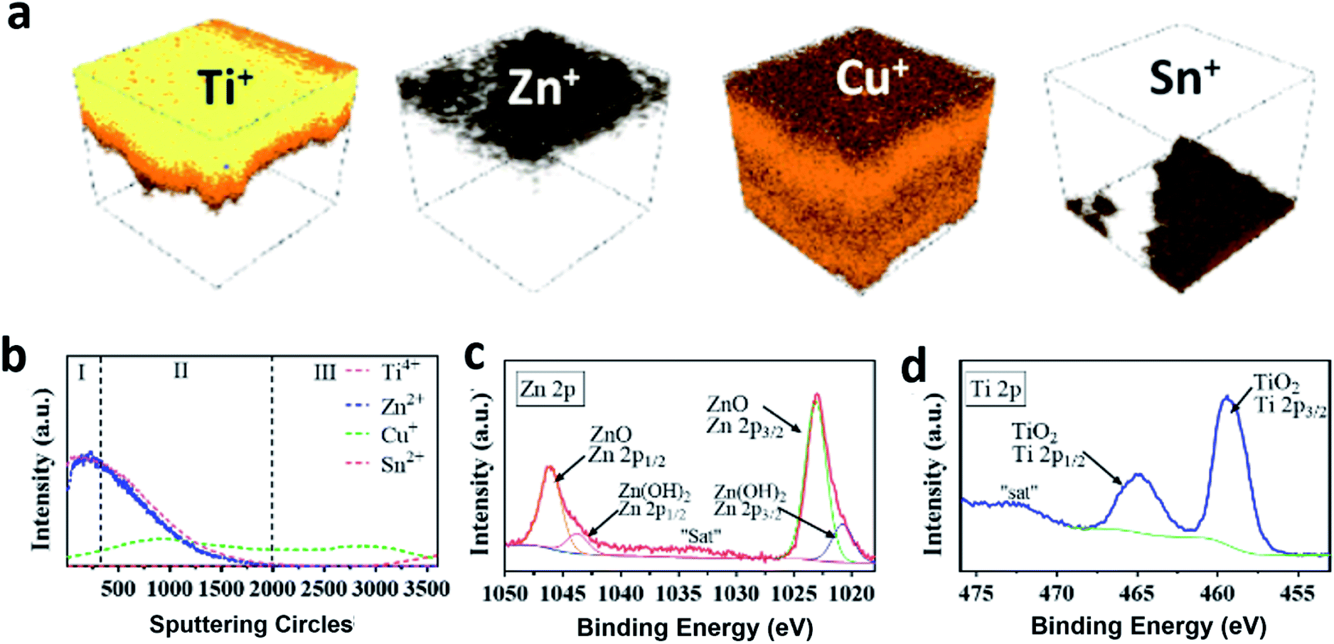 | ||
| Fig. 3 (a) 3D elemental rendering images and (b) corresponding XPS depth profile of the TiO2/ZnO/Cu2O composite structure by TOF-SIMS. Core-level XPS spectra of (c) Zn 2p for the ZnO/Cu2O photoelectrode and (d) Ti 2p for the TiO2/ZnO/Cu2O photoelectrode. The remark of “sat” means the satellite peak. | ||
Evaluation of photoelectrochemical activities
The photoelectrochemical performance of the prepared Cu2O photoelectrodes was evaluated under chopped visible-light illumination (>420 nm). To disclose the intrinsic benefits of surface coating on charge transport and stability properties, I–V and I–t curves for the prepared Cu2O photoelectrodes were recorded without a Pt cocatalyst in the first place. This is because Pt influences the charge transfer which may shield the intrinsic performance resulting from surface engineering. The LSV results also confirmed that Pt deposition does increase the photocurrent of Cu2O photocathodes even without surface protection (Fig. S4†). As shown in Fig. 4a, with the potential scan from 0 V to −0.6 V vs. Ag/AgCl (1 M KCl), the TiO2/Cu2O (blue line) sample shows slightly increased photocurrent densities compared to the bare Cu2O (black line). The TiO2/ZnO/Cu2O photoelectrode (red line) showed the highest photocurrent densities within the whole sweeping range, indicating the most efficient electron-extraction process induced by the ZnO layer among the prepared samples. Moreover, the dark current densities decreased in the order of Cu2O > TiO2/Cu2O > TiO2/ZnO/Cu2O at relatively higher applied potentials (>0.2 V vs. Ag/AgCl (1 M KCl)). Previous studies have suggested that the dark current can be ascribed to the corrosive reduction of Cu2O.10,36 The relatively lower and different values of TiO2/ZnO/Cu2O and TiO2/Cu2O photoelectrodes compared to the bare Cu2O indicate that the corrosive reactions of Cu2O are suppressed by TiO2/ZnO and TiO2 coatings but to the different extents.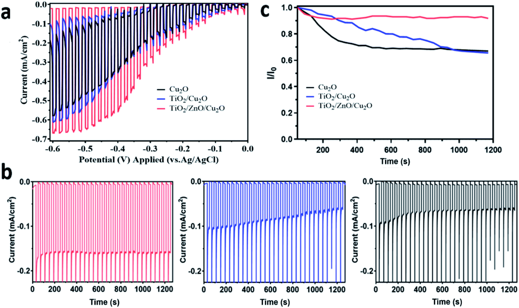 | ||
| Fig. 4 The photoelectrochemical performance of the prepared Cu2O (black), TiO2/Cu2O (blue) and TiO2/ZnO/Cu2O (red) photoelectrodes in 0.1 M Na2SO4 solution under visible-light irradiation (>420 nm) after purging with N2 for 0.5 h: (a) linear sweep voltammetry curves acquired at a scan rate of 2 mV s−1; (b) chronoamperometry measurements of the Cu2O-based photoelectrodes at −0.2 V vs. Ag/AgCl (1 M KCl); (c) normalized decay curve of the photocurrent density derived from the chronoamperometry results. | ||
The photocurrent densities of the photoelectrodes were further investigated by chronoamperometry at a constant bias of −0.2 V vs. Ag/AgCl (1 M KCl). As shown in Fig. 4b, the TiO2/ZnO/Cu2O photoelectrode exhibited a photocurrent density of −0.18 mA cm−2 which is not only higher than that of the bare Cu2O (−0.09 mA cm−2) but also has a 1.5-fold increase over the TiO2/Cu2O (−0.12 mA cm−2). The cathodic photocurrents obtained with TiO2/Cu2O photoelectrode were initially higher than those with the bare Cu2O but quickly decreased to a similar level, which indicates that the directly deposited TiO2 layer has a poor protective ability. The major cause of this instability is most likely to be the visible cracks within the TiO2 layer (as observed in Fig. 2c) since they allow the corrosive species to penetrate through the protective barrier and reach Cu2O. Once the Cu2O surface is corroded, Cu particles would grow at the Cu2O/TiO2 interface, thus blocking the charge transport and leading to the corrosion of Cu2O.49 Moreover, the pinholes and the resistive crystal boundaries in TiO2 can act as charge recombination centres (i.e. trap states), leading to poor stability.50 In contrast, the TiO2/ZnO/Cu2O photoelectrode shows much-improved stability with a negligible drop of photocurrent density under identical conditions (Fig. 4b). The decay curve of the prepared photoelectrodes is plotted in Fig. 4c. Clearly, the decay rate of photocurrent density increased in the order of TiO2/ZnO/Cu2O < TiO2/Cu2O < Cu2O within 1200 s of visible-light irradiation. The improved stability is mainly attributed to the continuous ZnO layer on Cu2O, which prevents cracking of the TiO2 layer, thus screening Cu2O from direct contact with the electrolyte. However, it has been reported that ZnO itself is not stable under the photoelectrochemical testing conditions,8 which is also further confirmed by the stability test (Fig. S5†) and the post-reaction SEM studies.
As shown in the post-reaction SEM images, bright particles were formed on the Cu2O grains in the irradiated area of the bare Cu2O and the TiO2/Cu2O photoelectrodes (Fig. S6a and c†), which are evidence of Cu2O corrosion to Cu particles.8 Moreover, without the protection of TiO2, the ultrathin ZnO layers disappeared and bright nanoparticles were also generated on Cu2O (Fig. S6b†). This suggests that the ZnO ultrathin layer itself cannot prevent the degradation of Cu2O under illumination, which is most likely caused by the dissolution of ZnO. In contrast, the TiO2/ZnO/Cu2O photoelectrode shows negligible surface variations under visible-light illumination (Fig. S6d†), thus testifying its superior resistance to corrosion. In addition, the results indicate that ZnO is an underlying layer protected by TiO2. The filling of the pre-formed ZnO layer into the cracked TiO2 coating of the TiO2/ZnO/Cu2O photoelectrode could be excluded.
For the non-Pt coated photoelectrodes, since the surface reaction kinetics for proton reduction is slow, the photocurrent densities obtained from the prepared Cu2O photoelectrodes can be either from proton reduction or oxygen reduction (even though the electrolyte was degassed for 30 min before the tests). To exclude the possibility of oxygen reduction, H2O2 as an important immediate and the possible product of oxygen reduction in the current system was measured by a UV-vis method (details in the ESI†). As shown in Fig. S7,† the UV-vis results showed no absorption at 350 nm, indicating the negligible amount of H2O2 generated by the prepared photoelectrodes during the reactions. Furthermore, the evolved H2 gas at the prepared photoelectrodes without a Pt cocatalyst at −0.2 V vs. Ag/AgCl (1 M KCl) for 3 h was determined by gas chromatography. The TiO2/ZnO/Cu2O photoelectrode generated H2 gas with an amount of 7.8 μmol corresponding to a calculated Faraday efficiency of 92.8%, thus indicating that the photocurrent of the TiO2/ZnO/Cu2O photoelectrode is mainly attributed to the proton reduction reactions. Negligible H2 products were detected for the bare Cu2O and the TiO2/Cu2O photoelectrodes. They are likely caused by the corrosive reactions that happened on Cu2O with the amount of H2 produced lower than the detection limit of gas chromatography.
The Faraday efficiency (FE) tests with Pt cocatalysts were further performed in a gas-tight H-cell reactor (details in the Experimental section). Pt cocatalysts were deposited on the photoelectrodes to improve the reaction kinetics for proton reduction. The SEM images of Pt modified photoelectrodes show tiny spherical nanoparticles deposited on the surface without changing the surface morphologies (Fig. S8†). The photocurrent densities of the prepared photoelectrodes were increased (Fig. S4†), as the Pt cocatalyst promotes surface reaction kinetics, increasing the charge transfer efficiency. The amounts of the evolved H2 gas and the FEs of the prepared photoelectrodes are summarised in Table S1.† The FEs of the prepared TiO2/ZnO/Cu2O and TiO2/Cu2O photoelectrodes with Pt cocatalysts were calculated to be 95.7% and 62.5%, respectively at −0.6 V vs. Ag/AgCl (1 M KCl) in a 1 h gas evolution reaction. The bare Cu2O and the ZnO/Cu2O photoelectrodes with Pt cocatalysts, however, produced negligible evolved H2 gas. The low FE of the TiO2/Cu2O and the non-detectable FE of the bare Cu2O and the ZnO/Cu2O samples can be caused by the corrosive reduction reactions of Cu2O and ZnO.
Mechanism elucidation
Since optoelectronic properties play a critical role in determining photoelectrochemical activity, Tauc plots derived from the UV-vis absorption spectra of the Cu2O and TiO2/ZnO/Cu2O are plotted in Fig. S9a and b,† respectively. The Tauc plots show that bare Cu2O and TiO2/ZnO/Cu2O have a similar band gap of ∼2.06 eV, in agreement with previously reported values.8 This indicates that the TiO2/ZnO coating does not alter the band structure of Cu2O. However, the corresponding UV-vis absorbance spectra (Fig. S8c†) show that the light-harvesting ability of Cu2O is decreased due to the surface coatings, indicating that there are other factors attributed to the enhanced performance.To understand the underlying reasons for the improved photoelectrochemical performance, TRPL measurements were further performed to investigate the electron transfer dynamics of the Cu2O, TiO2/Cu2O, and TiO2/ZnO/Cu2O photoelectrodes (Fig. 5). Each time-resolved fluorescence decay curve can be well fitted by a bi-exponential function  and effective lifetime can be calculated by
  where A1 and A2 are the amplitudes and τ1 and τ2 are the corresponding time constants of the fast and slow decay components, respectively. The electron dynamics is determined by the nonradiative and radiative recombination of electron–hole pairs, respectively.51,52 Note that the amorphous layers of TiO2 and ZnO are not excited at 405 nm and therefore, the observed fluorescence signals originate only from Cu2O. It is expected that nonradiative recombination will be dominated by the effective electron transfer, from the conduction band of Cu2O. Thus, the faster the decay, the higher the expected photoelectrochemical performance.29 As seen in Fig. 5, the TiO2/ZnO/Cu2O photoelectrode (red curve) exhibits the shortest lifetime (τ) of 1.513 ± 0.2 ns, consistent with its best performance, compared to TiO2/Cu2O (2.140 ± 0.2 ns, blue curve) and bare Cu2O (3.598 ± 0.2 ns, black curve). The fastest decay of the TiO2/ZnO/Cu2O photoelectrode indicates that the ultrathin ZnO layer between Cu2O and TiO2 facilitates the extraction of electrons to reduce electron-acceptors on the TiO2 surface, thus suppressing recombination losses and decreasing the chances of electrons remaining in the conduction band of Cu2O.51
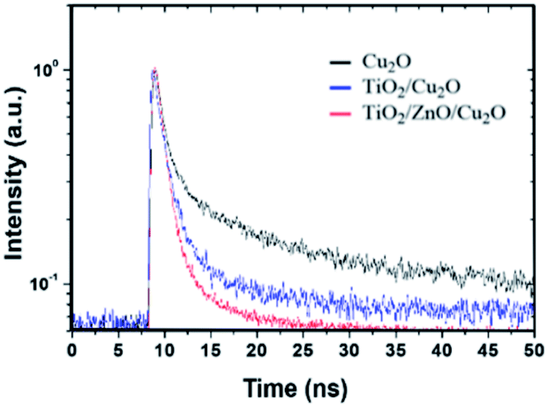 | ||
| Fig. 5 Time-resolved PL spectra acquired with an excitation wavelength of 405 nm for the prepared Cu2O (black), TiO2/Cu2O (blue) and TiO2/ZnO/Cu2O (red) photoelectrodes. | ||
The UV-vis and the TRPL results collectively elucidate the possible mechanism behind the enhanced performance of the TiO2/ZnO/Cu2O photoelectrode. Since the optical band structure of Cu2O is not significantly changed by the surface coating of TiO2 and ZnO, then in addition to the improved stability offered by the crack-free TiO2 layer, the improved photoelectrochemical activity and stability of the TiO2/ZnO/Cu2O photoelectrode can be ascribed to the efficient charge separation, supporting the beneficial role of the ZnO tunnel layer in extracting photoexcited electrons from the conduction band of Cu2O to the electrolyte, thus suppressing both recombination losses and corrosion of Cu2O.
Conclusions
In conclusion, a versatile method of pulsed electrodeposition has been developed to deposit a ZnO ultrathin layer on Cu2O. The TiO2/ZnO/Cu2O photoelectrode showed a 1.5-fold increase in photocurrent density and improved photostability compared to the TiO2/Cu2O photoelectrode. The ZnO buffer layer alleviated the visible cracks in the TiO2 protective layer, thus promoting the ability of TiO2 to suppress the corrosive reactions at the Cu2O–electrolyte interfaces. Moreover, the effective electron extraction by ZnO reduced the chances of photoexcited electrons staying in the conduction band of Cu2O (as evidenced by TRPL), resulting in a superior and more stable photoelectrochemical activity. The pulsed electrodeposition method is a valuable addition to the library of surface coating techniques to assemble composite photoelectrodes for solar energy utilisation.Conflicts of interest
There are no conflicts to declare.Acknowledgements
This project was financially supported by the Hong Kong Research Grant Council (RGC) General Research Fund GRF1305419 and the Australian Research Council Discovery Project (DP180102540). The authors appreciate the facilities and technical support provided by the UNSW Mark Wainwright Analytical Centre.Notes and references
- H. Wu, H. L. Tan, C. Y. Toe, J. Scott, L. Wang, R. Amal and Y. H. Ng, Adv. Mater., 2019, 1904717 CrossRef PubMed.
- C. Jiang, S. J. A. Moniz, A. Wang, T. Zhang and J. Tang, Chem. Soc. Rev., 2017, 46, 4645–4660 RSC.
- J. L. White, M. F. Baruch, J. E. Pander, Y. Hu, I. C. Fortmeyer, J. E. Park, T. Zhang, K. Liao, J. Gu, Y. Yan, T. W. Shaw, E. Abelev and A. B. Bocarsly, Chem. Rev., 2015, 115, 12888–12935 CrossRef CAS PubMed.
- W. Zou, L. Zhang, L. Liu, X. Wang, J. Sun, S. Wu, Y. Deng, C. Tang, F. Gao and L. Dong, Appl. Catal., B, 2016, 181, 495–503 CrossRef CAS.
- R. Wick and S. D. Tilley, J. Phys. Chem. C, 2015, 119, 26243–26257 CrossRef CAS.
- S. Hu, N. S. Lewis, J. W. Ager, J. Yang, J. R. McKone and N. C. Strandwitz, J. Phys. Chem. C, 2015, 119, 24201–24228 CrossRef CAS.
- X. Deng, R. LI, S. Wu, L. Wang, J. Hu, J. Ma, W. Jiang, N. Zhang, X. Zheng, C. Gao, L. Wang, Q. Zhang, J. Zhu and Y. Xiong, J. Am. Chem. Soc., 2019, 141, 10924–10929 CrossRef CAS PubMed.
- A. Paracchino, V. Laporte, K. Sivula, M. Grätzel and E. Thimsen, Nat. Mater., 2011, 10, 456–461 CrossRef CAS PubMed.
- Z. Zhang, R. Dua, L. Zhang, H. Zhu, H. Zhang and P. Wang, ACS Nano, 2013, 7, 1709–1717 CrossRef CAS PubMed.
- J. Luo, L. Steier, M. K. Son, M. Schreier, M. T. Mayer and M. Grätzel, Nano Lett., 2016, 16, 1848–1857 CrossRef CAS PubMed.
- C.-Y. Lin, Y.-H. Lai, D. Mersch and E. Reisner, Chem. Sci., 2012, 3, 3482 RSC.
- D. Liang, G. Han, Y. Zhang, S. Rao, S. Lu, H. Wang and Y. Xiang, Appl. Energy, 2016, 168, 544–549 CrossRef CAS.
- P. Wang, Y. H. Ng and R. Amal, Nanoscale, 2013, 5, 2952 RSC.
- A. A. Dubale, C.-J. Pan, A. G. Tamirat, H.-M. Chen, W.-N. Su, C.-H. Chen, J. Rick, D. W. Ayele, B. A. Aragaw, J.-F. Lee, Y.-W. Yang and B.-J. Hwang, J. Mater. Chem. A, 2015, 3, 12482–12499 RSC.
- C. Y. Toe, Z. Zheng, H. Wu, J. Scott, R. Amal and Y. H. Ng, J. Phys. Chem. C, 2018, 122, 14072–14081 CrossRef CAS.
- C. Y. Toe, Z. Zheng, H. Wu, J. Scott, R. Amal and Y. H. Ng, Angew. Chem., Int. Ed., 2018, 57, 13613–13617 CrossRef CAS PubMed.
- L. Yu, G. Li, X. Zhang, X. Ba, G. Shi, Y. Li, P. K. Wong, J. C. Yu and Y. Yu, ACS Catal., 2016, 6, 6444–6454 CrossRef CAS.
- X. An, K. Li and J. Tang, ChemSusChem, 2014, 7, 1086–1093 CrossRef CAS PubMed.
- P. D. Tran, S. K. Batabyal, S. S. Pramana, J. Barber, L. H. Wong and S. C. J. Loo, Nanoscale, 2012, 4, 3875 RSC.
- A. Martínez-García, V. K. Vendra, S. Sunkara, P. Haldankar, J. Jasinski and M. K. Sunkara, J. Mater. Chem. A, 2013, 1, 15235 RSC.
- L. A. Stern, L. Liardet, M. T. Mayer, C. G. Morales-Guio, M. Grätzel and X. Hu, Electrochim. Acta, 2017, 235, 311–316 CrossRef CAS.
- J. Azevedo, S. D. Tilley, M. Schreier, M. Stefik, C. Sousa, J. P. Araújo, A. Mendes, M. Grätzel and M. T. Mayer, Nano Energy, 2016, 24, 10–16 CrossRef CAS.
- M. Nishikawa, M. Fukuda, Y. Nakabayashi, N. Saito, N. Ogawa, T. Nakajima, K. Shinoda, T. Tsuchiya and Y. Nosaka, Appl. Surf. Sci., 2016, 363, 173–180 CrossRef CAS.
- C. Das, B. Ananthoju, A. K. Dhara, M. Aslam, S. K. Sarkar and K. R. Balasubramaniam, Adv. Mater. Interfaces, 2017, 4, 1–10 Search PubMed.
- C. Li, T. Hisatomi, O. Watanabe, M. Nakabayashi, N. Shibata, K. Domen and J.-J. Delaunay, Energy Environ. Sci., 2015, 8, 1493–1500 RSC.
- M. Schreier, J. Luo, P. Gao, T. Moehl, M. T. Mayer and M. Grätzel, J. Am. Chem. Soc., 2016, 138, 1938–1946 CrossRef CAS PubMed.
- J. Azevedo, L. Steier, P. Dias, M. Stefik, C. T. Sousa, J. P. Araújo, A. Mendes, M. Graetzel and S. D. Tilley, Energy Environ. Sci., 2014, 7, 4044–4052 RSC.
- C. G. Morales-Guio, S. D. Tilley, H. Vrubel, M. Grätzel and X. Hu, Nat. Commun., 2014, 5, 1–7 Search PubMed.
- Y. Lin, R. Kapadia, J. Yang, M. Zheng, K. Chen, M. Hettick, X. Yin, C. Battaglia, I. D. Sharp, J. W. Ager and A. Javey, J. Phys. Chem. C, 2015, 119, 2308–2313 CrossRef CAS.
- J. Gu, Y. Yan, J. L. Young, K. X. Steirer, N. R. Neale and J. A. Turner, Nat. Mater., 2015, 15, 456–460 CrossRef PubMed.
- B. Koo, S.-W. Nam, R. Haight, S. Kim, S. Oh, M. Cho, J. Oh, J. Y. Lee, B. T. Ahn and B. Shin, ACS Appl. Mater. Interfaces, 2017, 9, 5279–5287 CrossRef CAS PubMed.
- L. Rovelli, S. D. Tilley and K. Sivula, ACS Appl. Mater. Interfaces, 2013, 5, 8018–8024 CrossRef CAS PubMed.
- L. Steier, S. Bellani, H. C. Rojas, L. Pan, M. Laitinen, T. Sajavaara, F. Di Fonzo, M. Grätzel, M. R. Antognazza and M. T. Mayer, Sustainable Energy Fuels, 2017, 1, 1915–1920 RSC.
- Y. W. Chen, J. D. Prange, S. Dühnen, Y. Park, M. Gunji, C. E. D. Chidsey and P. C. McIntyre, Nat. Mater., 2011, 10, 539–544 CrossRef CAS PubMed.
- S. D. Standridge, G. C. Schatz and J. T. Hupp, Langmuir, 2009, 25, 2596–2600 CrossRef CAS PubMed.
- Y. Li, X. Zhong, K. Luo and Z. Shao, J. Mater. Chem. A, 2019, 7, 15593–15598 RSC.
- P. Dai, W. Li, J. Xie, Y. He, J. Thorne, G. McMahon, J. Zhan and D. Wang, Angew. Chem., Int. Ed., 2014, 53, 13493–13497 CrossRef CAS PubMed.
- P. Che, W. Liu, X. Chang, A. Wang and Y. Han, Nano Res., 2016, 9, 442–450 CrossRef CAS.
- D. Kang, T. W. Kim, S. R. Kubota, A. C. Cardiel, H. G. Cha and K. S. Choi, Chem. Rev., 2015, 115, 12839–12887 CrossRef CAS PubMed.
- P. De Luna, R. Quintero-Bermudez, C.-T. Dinh, M. B. Ross, O. S. Bushuyev, P. Todorović, T. Regier, S. O. Kelley, P. Yang and E. H. Sargent, Nat. Catal., 2018, 1, 103–110 CrossRef CAS.
- H. Y. Chung, W. Chen, X. Wen, J. N. Hart, H. Wu, Y. Lai, R. Amal and Y. H. Ng, Sci. Bull., 2018, 63, 990–996 CrossRef CAS.
- C. Ng, J.-H. Yun, H. L. Tan, H. Wu, R. Amal and Y. H. Ng, Sci. China Mater., 2018, 895, 1–10 Search PubMed.
- H. Wu, S. Li, X. Lu, C. Y. Toe, H. Y. Chung, Y. Tang, X. Lu, R. Amal, L. Li and Y. H. Ng, ChemPlusChem, 2018, 83, 934–940 CrossRef CAS PubMed.
- H. Wu, Z. Zheng, Y. Tang, N. M. Huang, R. Amal, H. N. Lim and Y. H. Ng, Sustainable Mater. Technol., 2018, 18, e00075 CrossRef CAS.
- P. Wang, H. Wu, Y. Tang, R. Amal and Y. H. Ng, J. Phys. Chem. C, 2015, 119, 26275–26282 CrossRef CAS.
- A. Paracchino, J. C. Brauer, J. E. Moser, E. Thimsen and M. Graetzel, J. Phys. Chem. C, 2012, 116, 7341–7350 CrossRef CAS.
- M. D. Susman, Y. Feldman, A. Vaskevich and I. Rubinstein, ACS Nano, 2014, 8, 162–174 CrossRef CAS PubMed.
- S. Hu, M. R. Shaner, J. A. Beardslee, M. Lichterman, S. Bruce and N. S. Lewis, Science, 2014, 344, 1005–1009 CrossRef CAS PubMed.
- M. A. Lumley, A. Radmilovic, Y. J. Jang, A. E. Lindberg and K.-S. Choi, J. Am. Chem. Soc., 2019, 141, 18358–18369 CrossRef CAS PubMed.
- A. B. Wang, M. Zhang, X. Cui, Z. Wang, Y. Yang, Z. L. Wang and Z. Lin, Angew. Chem., Int. Ed., 2020, 59, 1611–1618 CrossRef PubMed.
- X. Wu, J. N. Hart, X. Wen, L. Wang, Y. Du, S. X. Dou, Y. H. Ng, R. Amal and J. Scott, ACS Appl. Mater. Interfaces, 2018, 10, 9342–9352 CrossRef CAS PubMed.
- H. L. Tan, H. A. Tahini, X. Wen, R. J. Wong, X. Tan, A. Iwase, A. Kudo, R. Amal, S. C. Smith and Y. H. Ng, Small, 2016, 5295–5302 CrossRef CAS PubMed.
Footnote |
| † Electronic supplementary information (ESI) available: Fig. S1–S5. See DOI: 10.1039/d0ta00629g |
| This journal is © The Royal Society of Chemistry 2020 |