
 Open Access Article
 This Open Access Article is licensed under a
 Creative Commons Attribution 3.0 Unported Licence
Metal–organic framework nanosheets for enhanced performance of organic photovoltaic cells†
Kezia
Sasitharan
a,
David G.
Bossanyi
 b,
Naoum
Vaenas
b,
Andrew J.
Parnell
b,
Jenny
Clark
b,
Ahmed
Iraqi
a,
David G.
Lidzey
b and
Jonathan A.
Foster
*a
b,
Naoum
Vaenas
b,
Andrew J.
Parnell
b,
Jenny
Clark
b,
Ahmed
Iraqi
a,
David G.
Lidzey
b and
Jonathan A.
Foster
*a
aDepartment of Chemistry, The University of Sheffield, Dainton Building, Brook Hill, S3 7HF, Sheffield, UK. E-mail: jona.foster@sheffield.ac.uk
bDepartment of Physics and Astronomy, The University of Sheffield, Hicks Building, Hounsfield Road, S3 7RH, Sheffield, UK
First published on 10th March 2020
Abstract
Metal–organic framework nanosheets (MONs) are an emerging class of two-dimensional materials whose diverse and readily tunable structures make them ideal for use in optoelectronic applications. Here, liquid exfoliation is used to synthesize ultrathin zinc-porphyrin based MONs with electronic and optical properties ideally suited for incorporation into a polythiophene–fullerene (P3HT–PCBM) organic solar cell. Remarkably, the addition of MONs to the photoactive layer of a photovoltaic device results in a power conversion efficiency of 5.2%, almost twice that for reference devices without nanosheets with a simultaneous improvement of Jsc, Voc and FF. Our analysis indicates that the complimentary electronic, optical and structural properties of the MONs allows them to act as a surface to template the crystallization of P3HT leading to a doubling of the absorbance, a tenfold increase in hole mobility and reduced grain size. These results demonstrate the potential of MONs as a tunable class of two-dimensional materials for enhancing the performance of a broad range of organic solar cells and other electronic devices.
1 Introduction
Two-dimensional nanomaterials such as graphene hold enormous potential for use in advanced electronics, energy, separation and composite materials applications.1–3 However, the simple chemical composition of many of these materials mean it can be difficult to optimise them for many applications. Metal–organic framework nanosheets (MONs) are an emerging class of two-dimensional nanomaterials composed of organic linkers coordinated to metal-ions or clusters.4–7 MONs display the high surface areas and aspect ratios of other two-dimensional materials but have a modular structure which readily allows for systematic tuning of their electronic, optical and mechanical properties and introduction of new chemical functionalities. A diverse range of MONs have been formed either bottom-up, via an arrested crystallization in the presence of a templating agent or interface, or “top-down” by mechanical or liquid exfoliation of layered metal–organic frameworks (MOFs). MONs have already shown significant promise for use in a variety of separation,8,9 catalysis,10,11 sensing9,12–14 and electronics applications.15–19Organic photovoltaics (OPV) offer a variety of attractive properties over current silicon technology, including highly tuneable structures, low cost production, large area manufacturing capability and the potential to create flexible and semi-transparent devices.20 Historically OPV has suffered from low power conversion efficiencies and poor stability but there has been renewed interest thanks to recent innovations such as new materials21,22 device architectures23 and multicomponent (ternary or quaternary) bulk heterojunction (BHJ) approaches.24–29 In the latter case, a wide range of additives have been investigated whose complimentary optical or electronic properties enable them to enhance the range of light absorbed,30–32 facilitate more efficient electron or hole transport33 or modify the morphology of the devices leading to improvements in performance and stability.34–36 Two-dimensional materials are ideal candidates for use as additives thanks to their large surface areas and distinct electronic and optical properties.37–39 Transition metal dichalcogenides (TMDCs) in particular have attracted significant interest because of their thickness-dependant opto-electronic properties,40 ambipolar charge transport,41 chemical stability and direct band-gaps in the single layer form.42 However, the difficulties in controlling layer thickness and scalability of these materials have so far limited their use in OPV applications.43
MONs possess a variety of characteristics that make them attractive candidates for use in photovoltaics, as outlined in the “MOF electronic roadmap”.44 Their diverse chemistry and modular structures allow for ready tuning of their optical and electronic properties. This means MONs have the potential to perform roles in light absorption, carrier generation and transport within PV devices. MONs have a long range order which could help minimize the traps, dead ends and defects problematic in light-harvesting organic polymers. The nanoscopic dimensions of MONs open up new possibilities for their inclusion within the active layer of thin film devices and the highly anisotropic structure of MONs mean they are predisposed to align parallel to the surface.
Most work using MOFs for photovoltaics has focused on their use in dye-sensitized solar cells where they have been used to reduce structural disorder and increase charge mobility.45–47 They have achieved this using either dyes or donor–acceptor molecules as ligands within the MOFs or by incorporating dyes or fullerenes within their pores with power conversion efficiencies reported up to 1.27%.48,49 Epitaxially grown MOF films have also been employed as donor layers in planar light-harvesting devices.50–53 MONs have shown promise in a variety of electronic applications,18,54 however we are only aware of two reports of their use in solar cells. One recent report showed that tellurophene based MONs can be blended with ZnO-PEIE (polyethylenimine ethoxylate) to form a buffer layer which resulted in a small enhancement in the performance of two OPV devices.55 In another recent study, porphyrin based MON films were formed on ITO using a Langmuir–Blodgett approach and impregnated with C60 to form a liquid junction solar cell with quantum efficiency less than 0.1%.56 To-date, there have been no-reports of the use of MONs or more generally MOFs within the active layer of bulk-heterojunction OPV devices.
Here, we explore a new approach to enhancing OPV bulk heterojunction devices by blending 2D metal–organic nanosheets along with semi-conducting polymers and fullerene acceptors in the photoactive layer via a simple spin-coating procedure. We hypothesized that zinc-porphyrin based MONs would have good electronic and optical properties for inclusion in OPV devices and used ultrasonic liquid exfoliation to create predominantly monolayer nanosheets. Remarkably, addition of the MONs to a well-studied OPV system was found to result in an almost doubling of the device performance compared to the reference devices without MONs. Detailed studies were therefore undertaken in order to understand the role of the MONs on device performance, charge mobility, absorbance, thin film morphology and crystallinity. On the basis of these observations we were able to put forward a model to explain the improvements in performance seen. We anticipate that the diverse and tunable properties of MONs will enable them to play an important role in enhancing the performance of a wide range of other OPV and electronic devices.
2 Results and discussion
2.1 Synthesis and characterisation of the zinc porphyrin MONs
The layered MOF Zn2(ZnTCPP), where TCPP is tetrakis(4-carboxyphenyl)porphyrin, was synthesised solvothermally using a procedure adapted from Choi et al.57 (Fig. 1a). TCPP was heated with zinc nitrate in a DMF![[thin space (1/6-em)]](https://www.rsc.org/images/entities/char_2009.gif) :ethanol mixture at 80 °C for 24 h to produce a black microcrystalline powder. XRPD and other solid-state analysis (Fig. S1–S3, ESI†) showed a good match for the previously reported Zn2(ZnTCPP) and analogous structures in literature.13,58–62
:ethanol mixture at 80 °C for 24 h to produce a black microcrystalline powder. XRPD and other solid-state analysis (Fig. S1–S3, ESI†) showed a good match for the previously reported Zn2(ZnTCPP) and analogous structures in literature.13,58–62
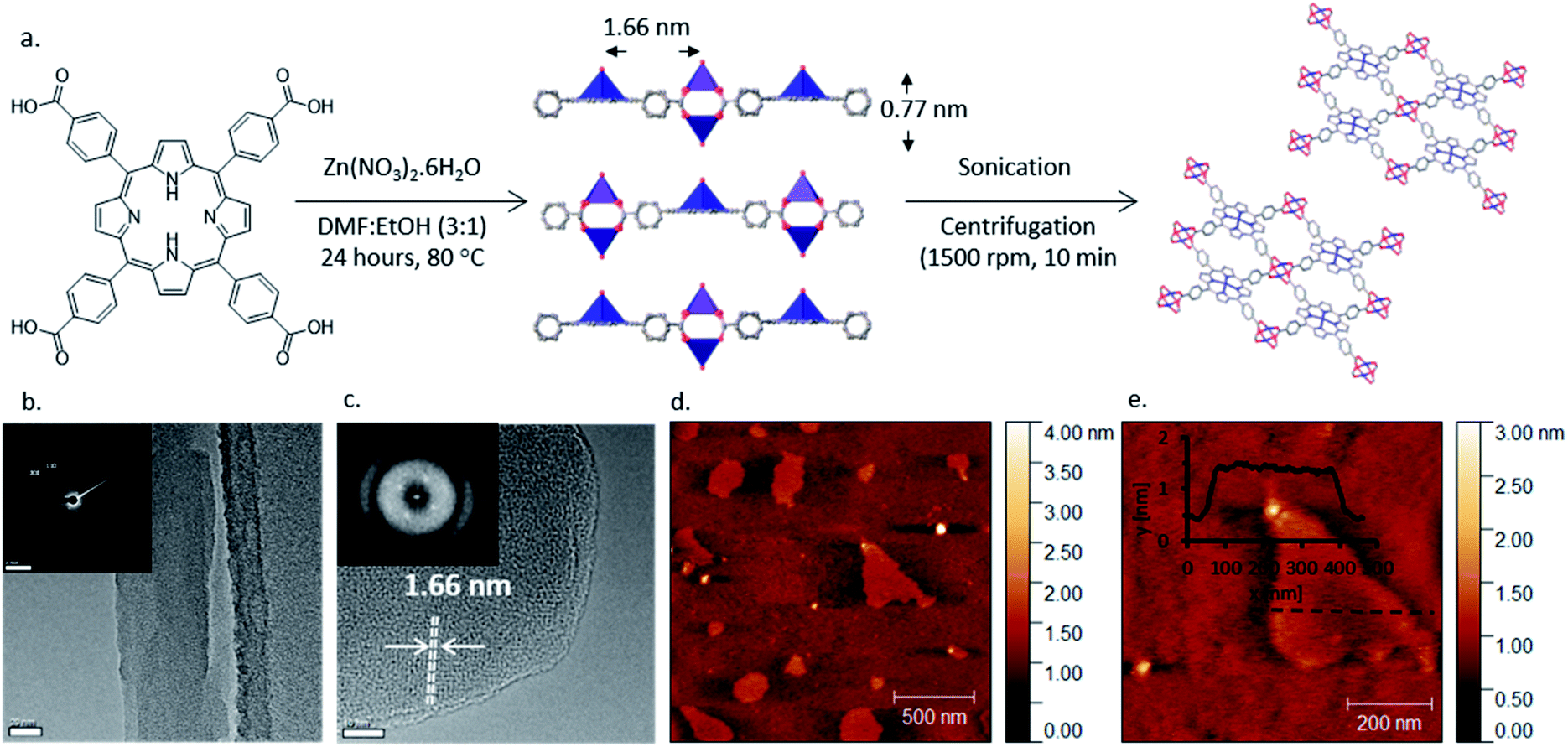 | ||
| Fig. 1 Synthesis and morphological characterisation of Zn2(ZnTCPP) MONs; (a) scheme showing synthesis of the layered MOF Zn2(ZnTCPP) followed by liquid exfoliation into MONs; (b) transmission electron micrograph of a single nanosheet on the TEM grid; (b-inset): single-area electron diffraction pattern of the nanosheets; (c) HR-TEM image of a nanosheet showing lattice fringe distance = 1.66 nm (inset: the corresponding FFT pattern); (d) AFM topographical image of the MONs as observed under a 1.5 μm area scan; (e) AFM image of a single MON with the corresponding height profile as inset (0.77 nm thickness; 300 nm lateral dimension). | ||
The layered MOF was suspended in chlorobenzene (5 mg ml−1), sonicated in an ultrasonic bath for 1 hour and centrifuged at 1500 rpm for 10 min to remove larger particles. The resulting transparent suspension showed Tyndall scattering (Fig. S4, ESI†) consistent with the presence of nanoparticles. Atomic force microscopy (AFM) and Transmission Electron Microscopy (TEM) revealed the formation of ultra-thin nanosheets with lateral dimension of 300 ± 100 nm and a uniform thickness of 1 ± 0.3 nm corresponding to predominantly monolayer thickness (Fig. 1a, S5 and S6, ESI†). Fast Fourier Transform (FFT) of electron diffraction patterns (Fig. 1c) show lattice fringes with spacing of 1.66 nm consistent with the Zn–Zn distance in the MON structure (Fig. 1c). Electron energy loss spectroscopy (EELS) showed the zero-electron loss peak to be the most intense with an inelastic mean free path of 0.10, consistent with the observation of a sample of monolayer thickness (Fig. S6c, ESI†). It is worth noting that the MONs produced by our simple and scalable approach are thinner and have smaller lateral dimensions than those typically obtained from TCPP with Zinc and other metal ions (Cu, Co, Cd) including assembly at liquid interfaces,59,60,62 intercalation of ligands63 and surfactant assisted synthesis.13
UV-Vis spectra of the Zn2(ZnTCPP) MONs in suspension show they are strongly absorbing with a characteristic π–π* soret band at 435 nm and Q bands at 564 and 601 nm (Fig. S7, ESI†). Fig. 2a shows the thin film UV-Vis spectra on quartz substrates in which the band at 440 nm is assigned as the π–π* peak, slightly red shifted compared to the MON in suspension, whilst Q bands are seen at 563 and 605 nm respectively.64 The electrochemical properties of the MONs were studied in acetonitrile using cyclic voltammetry (CV) and the key results are shown in Fig. 2d. The HOMO–LUMO energy level calculations derived from the onset of oxidation and reduction are shown in Fig. S8, ESI.† The nanosheets show an electrochemical band gap of 1.8 eV making it a good material for light harvesting applications. Previous literature reports have shown that a minimum energy offset of 0.3 eV between the LUMO of the donor and acceptor is necessary to facilitate efficient exciton dissociation.65 The LUMO level of the MONs was found to be −3.5 eV which makes it ideally positioned between that of the fullerene electron acceptor [6,6]-phenyl-C61-butyric acid methyl ester (PCBM) at −3.80 eV and electron donating organic polymer poly(3-hexylthiophene-2,5diyl) (P3HT) at −3.00 eV.66 These finding lead us to evaluate P3HT–Zn2(ZnTCPP)–PC60BM ternary blend organic photovoltaics where all three of the materials in the active layer display an energy offset in the excess of the 0.3 eV limit. Although the high band-gap of P3HT means that the performance of these systems is ultimately limited, as a well-studied BHJ system it provides an ideal test-bed to investigate our novel materials and rationally understand any changes in the observed performance.
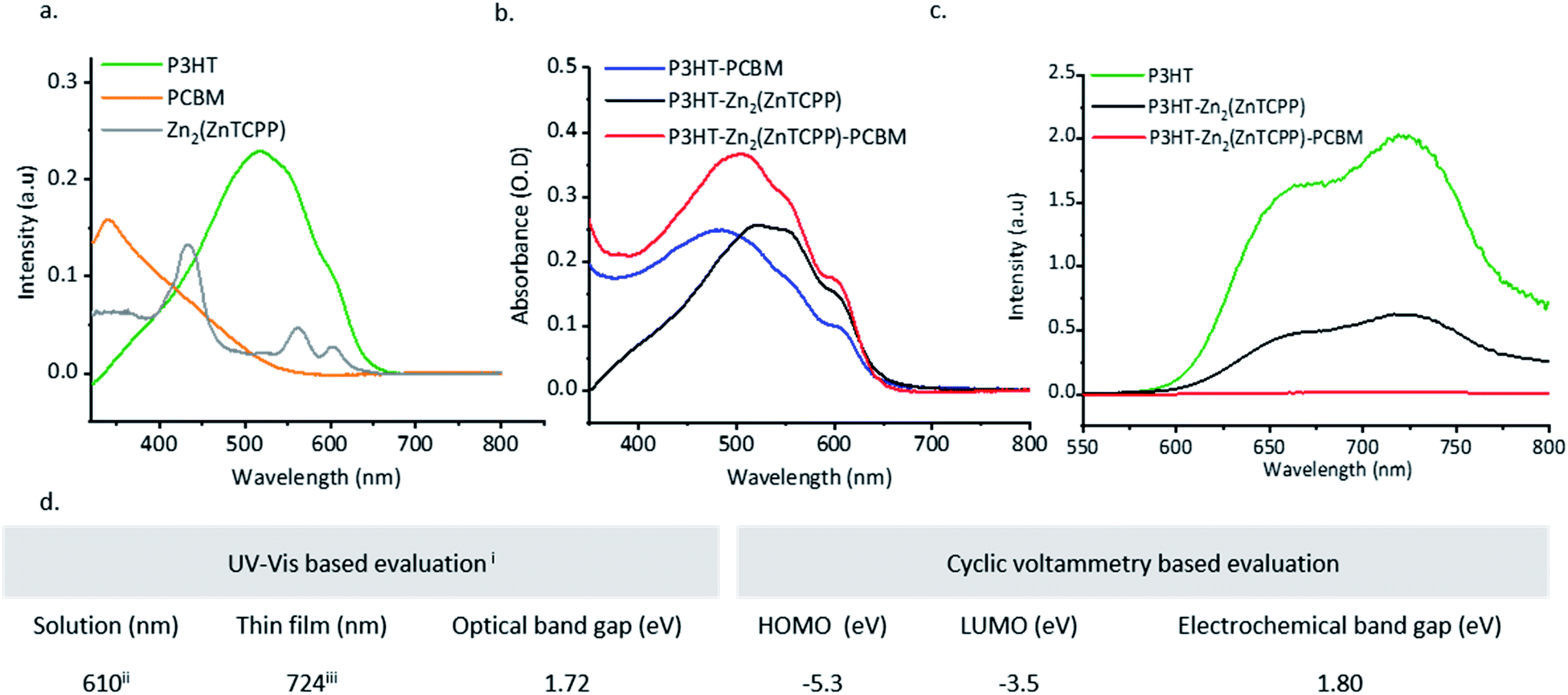 | ||
| Fig. 2 Optoelectronic characterizations: (a) thin film absorption spectra of P3HT and PCBM spin-coated from chlorobenzene at 2000 rpm@60 seconds and Zn2(ZnTCPP) MONs dropcast (5 mg ml−1) and dried (b) comparison of absorption spectra of the polymer–fullerene, polymer–nanosheets and polymer–nanosheets–fullerene blends all spin-coated to achieve a layer thickness of ∼150 nm; (c) photoluminescence spectra recorded from spin coated thin films (∼150 nm) of P3HT, P3HT–Zn2(ZnTCPP) and P3HT–Zn2(ZnTCPP)–PCBM blends, excited at 500 nm. Refer to Fig. S13 (ESI†) for spin coating parameters used; (d) table showing key results from the band gap evaluation of Zn2(ZnTCPP) MONs (i) λonset values obtained by extrapolating the charge transfer peak to the x-axis (shown in Fig. S9, ESI†); (ii) the charge transfer UV-Vis peak as observed in Fig. S7;† (iii) a MON suspension (5 mg ml−1 in ethanol) was dropcast onto a quartz substrate, followed by solvent evaporation prior to recording the UV-Vis spectra. | ||
Solution and thin-film photoluminescence (PL) studies were undertaken in order to understand the energy transfer characteristics between the MONs and the chosen donor–acceptor components. The MONs show a broad PL emission between 500–800 nm which was quenched upon gradual addition of PCBM (Fig. S10, ESI†). In the solution state PL, addition of MONs to P3HT resulted in 70% quenching of the P3HT signal and a 30% increase in the PL signal of the MONs (Fig. S11, ESI†). This observation is consistent with previous literature studies in ternary blend solar cells.67,68 The PL intensity of pristine-P3HT films when compared with that of P3HT–MONs blend films was found to be quenched (69.6% quenching efficiency, obtained by integrating the area under curve) with the addition of MONs. When PC60BM is introduced into the blend, complete quenching of the PL signal is observed (Fig. 2c). Fig. S12, ESI† shows the systematic study of PL quenching of P3HT thin films upon gradual increase in the weight ratio of incorporated MONs which saturates at a ratio of 1:0.5 P3HT:Zn2(ZnTCPP).
2.2 Device fabrication, optimisation and performance
The blends were deposited by spin coating on ITO coated glass substrates containing a 30–40 nm thick layer of PEDOT:PSS. The spin coating parameters were adjusted in order to obtain a ∼150–200 nm thick photoactive layer. Finally, a 5 nm thick BCP (2,9-dimethyl-4,7-diphenyl-1,10-phenanthroline, commonly known as bathocuproine) buffer layer and a 100 nm thick Ag electrode was thermally evaporated on top and the devices were encapsulated with glass covers. The current density–voltage curves under illumination with a solar simulator (AM 1.5, 1SUN) for the blends P3HT:Zn2(ZnTCPP):PCBM and control P3HT–PCBM are shown in Fig. 3b for the optimised device. Remarkably, the power conversion efficiency (PCE) of the best performing optimised devices with nanosheets was 5.2%; the highest value reported in the literature for this type of device (Fig. 3b) and twice that reported for the best performing device without nanosheets (2.67%). The best performing optimised device with the nanosheets exhibited a short circuit current density (Jsc) of 10.8 mA cm−2, open circuit voltage (Voc) of 0.69 V and fill factor (FF) of 69% corresponding to a PCE of 5.2%. These results are also remarkably reproducible with a low standard deviation of 0.12% PCE across 35 devices developed. The laser beam induced current (LBIC) mapping of the MON based devices shows uniform current distribution throughout the mapped region (Fig. 3c).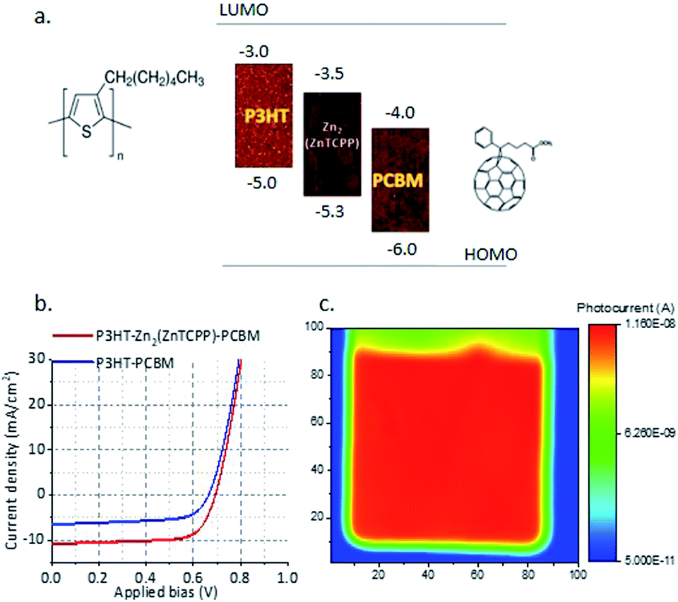 | ||
| Fig. 3 Device performance metrics; (a) a representation of the HOMO–LUMO level alignment of the components of the ternary device; (b) J–V curve of the best performing devices with and without the MONs; (c) high resolution LBIC mapping of the P3HT–MON–PCBM device showing a uniform distribution of current over the entire mapped region, each division on the axes corresponds to the step size = 25 microns. | ||
Table S1 (ESI†) details the iterative development of the devices, varying the ratio of materials and annealing protocols. It is worth noting that as the concentration of MONs in the blend is increased from 1:0.25:1 to 1:0.5:1 (P3HT:Zn2(ZnTCPP):PCBM) weight ratio (Table S1a–d),† the Voc remains unchanged within error, and the Jsc increases by 2.08 mA cm−2 accompanied by a 2% increase in the fill factor which corresponds to higher power conversion efficiency. This increase in PCE with the gradual increase in the amount of MONs indicates that the MONs play a significant role in controlling the device performance. Upon further increase of the MON concentration (1:1:1), there is a significant drop in the FF and PCE. Thus 1:0.5:1 weight ratio of P3HT:Zn2(ZnTCPP):PCBM was fixed as the optimum blend concentration for the nanosheet based devices. The reference devices produced under the same conditions without MONs were consistently lower across all metrics with the best performing optimised device without nanosheets exhibited a Jsc of 7.09 mA cm−2, Voc of 0.66 V and FF of 57.44% corresponding to a power conversion efficiency of 2.67%. A comparison with data reported in the literature for P3HT–PCBM based device having active layer-BCP-Ag configuration show a broad spread of values across the 38 device results statistically analysed in this work (Table S2, ESI†). In addition to remarkably high PCE's, the Jsc values of our devices are notably high in comparison to previous literature reports indicating higher current density with the incorporation of MONs. Importantly, reference devices with the bulk unexfoliated MOF incorporated into the active layer were not found to function, presumably because of short circuiting due to the μm sized MOFs. This establishes that the nanoscopic dimensions of the monolayer MOF nanosheets play a key role in device performance. A control device was also made by incorporating the TCPP ligand in the P3HT–PCBM blend and the performance was comparable with the P3HT–PCBM devices with a PCE of 1.93% (Jsc = 6.5 mA cm−2, Voc = 0.54 V; FF = 55%) (Fig. S16, ESI†). Progressive enhancement in the Jsc and PCE and no change in Voc was observed when both sets of devices were subjected to thermal, solvent and solvent + thermal annealing conditions as shown in Fig. 4 and listed in Table S1, ESI.† Interestingly, the fill factor for the as cast MON devices is significantly improved compared to the reference devices but the gap narrows slightly with the additional annealing processes.
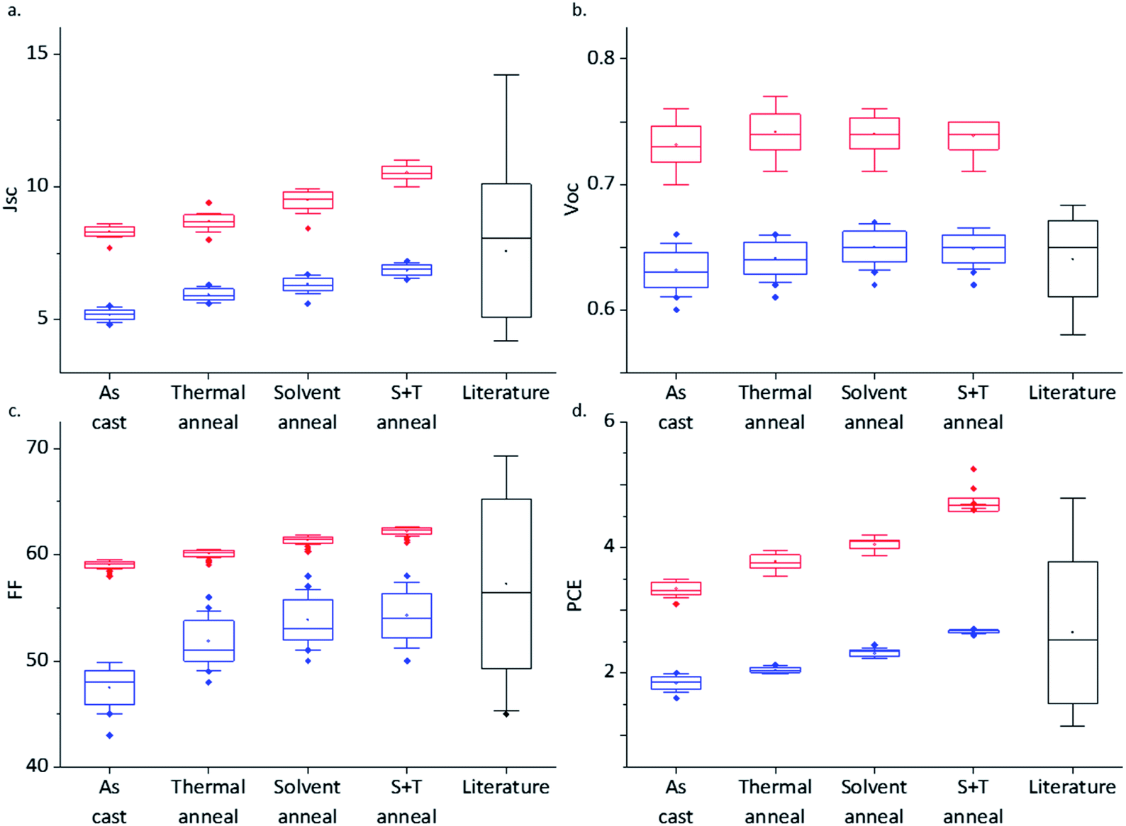 | ||
| Fig. 4 Statistical analysis of device performance metrics; Comparison of variation of −Jsc (a), Voc (b), FF (c) and PCE (d) of the MON based devices (red) with the reference devices (blue) and previous literature reports (black) represented as box plot. | ||
2.3 Absorption and charge mobility
External quantum efficiency (EQE) measurements were done to compare the amount of current generation from the devices when irradiated in the wavelength range (400–700 nm). Comparison of EQE measurements for the MON-based devices with the control devices (Fig. 5a) shows enhanced spectral response around 430–450 nm corresponding to π–π* transition absorption of the MONs and another well pronounced enhancement at 550–580 nm corresponding to the Q absorption band of the MONs.64 A higher absorption in the region 600–630 nm corresponds to an increased percentage of crystalline polymer structures in the film.69 A decrease in the amorphous P3HT region (Fig. 5b) and the red-shifted λmax of the normalized absorption spectra of the MON incorporated ternary blend (Fig. 5b) supports this analysis.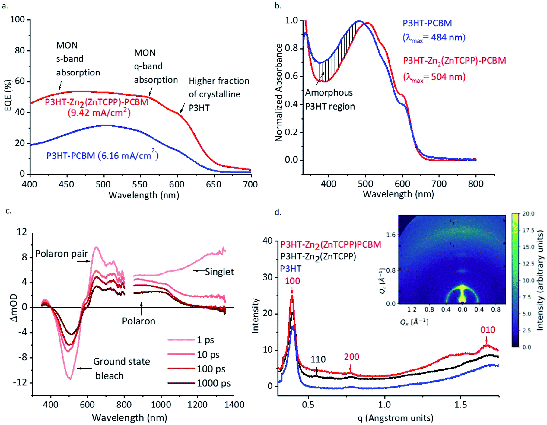 | ||
| Fig. 5 EQE, absorption and GI-WAXS results: (a) EQE spectra of the MON based devices and the reference devices (with the integrated Jsc values); (b) comparison of the normalized absorption spectra of the reference active layer and the MON based ternary blend-showing a decrease in the amount of amorphous P3HT upon incorporation of MONs; (c) transient absorption spectra of from P3HT–Zn2(ZnTCPP)–PCBM blend; (d) the 1D cross-sectional analysis of GI-WAXS signals from pristine P3HT and P3HT–Zn2(ZnTCPP) blend film overlaid with the signal from P3HT–Zn2(ZnTCPP)–PCBM active layer blend processed according to the device optimisation procedure; (inset: 2D detector image of P3HT–Zn2(ZnTCPP)). | ||
No obvious new transient-absorption (TA) features were observed when Zn2(ZnTCPP) was added to the blend. However, the signal for the sample with Zn2(ZnTCPP) added is roughly twice that of the sample without (Fig. 5c, S17a and b ESI†). This gives evidence of enhanced light absorption in the blend with the nanosheets, corresponding to higher current density in the solar cell performance. Evaluation of kinetics of the P3HT–PCBM and P3HT–Zn2(ZnTCPP)–PCBM blends show no real change in the excited state dynamics upon addition of Zn2(ZnTCPP), at least on timescales ranging from 1 ps to 1 ns (Fig. S18a†). However, the kinetics of polaron pairs in P3HT shows that the addition of Zn2(ZnTCPP) indicates a large increase (more than twofold) in the population of charges in P3HT (Fig. S18b†).
The charge carrier mobility of electrons and holes after dissociation of excitons at the donor/acceptor interface is an important factor in bulk-heterojunction PV performance. Space-charge limited currents (SCLC) were fabricated and tested in hole only and electron only devices (Table S3 and Fig. S19a–S22b†).70 In the absence of nanosheets, the electron mobility in P3HT–PCBM is higher by an order of magnitude than the hole mobility. This can lead to unbalanced charge transport and non-geminate recombination. The inclusion of MONs increases the hole mobility of the system by a factor of 10, improving the balance of hole and electron mobility within the devices. This enables more efficient extraction of charges during transport to the electrodes reducing the opportunity for free charges to encounter each other and recombine at the donor–acceptor interface.
2.4 Understanding the morphology – GIWAXS and AFM
Grazing Incidence Wide Angle X-ray Scattering (GI-WAXS) measurements were performed on ∼150 nm thick films with and without nanosheet in order to probe the structure of the thin films used in the devices (Fig. 5d and S23†). Peak at 0.55 Å corresponds to reflection peaks (110) from Zn2(ZnTCPP) nanosheets57 which confirms that the nanosheets do not degrade in the presence of the polymer or during the high temperature anneal but facilitate a well-ordered arrangement of the polymer chains and enhance the crystallinity. The peak corresponding to (100) reflections of P3HT is observed with an enhanced intensity in the GI-WAXS signal from P3HT– Zn2(ZnTCPP) film. P3HT appears to have predominantly adopted a face on orientation with respect to the substrate with an intense lamellar stacking peak in plane (100) along qx. The crystallite size of P3HT was calculated to be 13.59 nm from the 100 and 110 peaks using Scherrer analysis (Table S4, ESI†). These observations indicate a higher fraction of crystalline P3HT upon the inclusion of Zn2(ZnTCPP), consistent with the observed changes in absorption spectra.AFM imaging of P3HT–Zn2(ZnTCPP)–PCBM spin coated blends shows the MONs to be homogeneously distributed throughout the matrix of P3HT–PCBM. Demixing of P3HT and PCBM during thin film formation leads to separate regions of P3HT rich and PCBM rich nanoscale domains.71 A spatial Fourier transform was used to extract the phase separation length scales (grain size) from the AFM images (Fig. S25 and S26, ESI†). In the reference P3HT–PCBM active layer these are in the range of 10–15 nm, while in the presence of MONs the length scale is 6–10 nm. In the presence of MONs, the grain sizes are smaller and more well defined which we speculate favours charge carrier transport. It has been previously shown that the overgrowth of PCBM aggregates (in some literature reports micron sized PCBM crystallites have been observed) correlate with degraded power conversion efficiency and is a reason for detrimental performance in fullerene based systems.72 The presence of an additional 2D component which interacts closely with both P3HT and PCBM appears to inhibit their de-mixing and act as a barrier to prevent the formation of oversized PCBM aggregates.
3 Discussion of the role of MONs within the devices
The zinc-porphyrin MONs possess a number of features that make them ideally suited for incorporation as third component into the active layer of OPVs. The nanoscopic dimensions of the MONs, predominantly monolayer in thickness and ∼300 nm wide, allows for their incorporation at high concentrations (20 wt%) within the ∼150 nm thick active layer of the devices. It is worth emphasising that devices based on the bulk MOF did not function and it is only because the predominantly monolayer nanosheets have thicknesses less than the exciton diffusion length that they are able to be incorporated into BHJ type architecture. The porphyrin units have an absorption maximum between that of PCBM and P3HT which means the ternary blends are able to capture a larger fraction of the incident solar spectrum, although this remains dominated by the more strongly absorbing P3HT. The LUMO of the MONs at −3.5 eV means they are ideally positioned between those of PCBM (−4.00 eV) and P3HT (−3.00 eV) with a greater than 0.3 eV offset potentially allowing the MONs to facilitate an energy cascade. However, the transient absorption spectra do not show any of the new features upon inclusion of the MONs that might be expected if the nanosheets are involved in the charge/energy transfer process. This indicates that either charge transfer to the MONs does not happen, or that it occurs faster than the limit of the experimental set-up. Nevertheless, there is typically a trade-off between improvements in Jsc/FF and Voc in ternary devices where additives improve device morphology, but the misaligned HOMO–LUMO levels between the corresponding levels of the donor and acceptor materials leads to reduced exciton dissociation and charge transfer rates. The very strong device performance and in particular the fact that the Voc is close to the theoretical limit for this system indicates that intermediate HOMO–LUMO level of the MONs prevents geminate recombination losses which would otherwise limit device performance.The addition of nanosheets also impacts significantly on the morphology of the device. Absorbance, EQE, GI-WAXS and ellipsometry studies indicate that incorporation of the nanosheets results in a larger fraction of crystalline P3HT regions whilst smaller P3HT–PCBM grain sizes are seen by AFM. These observations could also account for the increased hole mobility observed in charge mobility studies and the increase in the population of charges in P3HT observed in transient absorption studies in the presence of MONs. The improved matching of the hole and electron mobilities and smaller grain sizes would reduce the chances for charge carrier recombination during transport to the electrodes.70 These observations indicate that the two-dimensional MONs act as a surface to template the formation of a larger fraction of crystalline P3HT domains and barriers to inhibit the overgrowth of PCBM aggregates leading to smaller grain sizes (Fig. 6). Thus the role of the MONs is to enhance the morphology of the active layer without hindering the formation, dissociation and transport of the charge carriers through the charge percolation pathways.
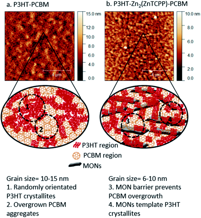 | ||
| Fig. 6 AFM images showing optimised devices following solvent and thermal annealing with (right) and without (left) MONs and corresponding cartoons highlighting the role of the nanosheets in creating smaller and more crystalline P3HT domains and inhibiting the overgrowth of PCBM aggregates. | ||
4 Conclusions
Here we have demonstrated the first example of a MON based bulk-heterojunction solar cell by incorporating monolayer Zn2(ZnTCPP) MONs in the active layer blend of P3HT:PCBM. The MONs' intermediate energy levels with respect to the donor and acceptor system means that they do not create traps for charges, as observed with the introduction of nanomaterials in other ternary systems. The efficiency of the best performing devices with a 20% loading of MONs was 5.2%, almost double that of the reference devices without nanosheets (2.67%) and the highest performing devices of its class. Incorporation of the MONs leads to a significant improvement of the open circuit voltage, current density and fill factor of the solar cells. Absorption, EQE, GI-WAXS, ellipsometry and AFM studies show a tenfold increase in charge mobility, doubling of the absorbance, improved crystallinity of P3HT and reduced P3HT:PCBM domain sizes. We suggest that these observations are best explained by the MONs acting as a template to the formation of P3HT crystallites and as a barrier to prevent the over-growth of PCBM. These results demonstrate the potential of MONs as a new class of two-dimensional nanomaterials for use in optoelectronic devices.The ease with which the electronic and optical properties of MONs can be tuned mean that the band-gap of these materials can potentially be optimized to blend with any polymer system of choice, potentially with non-fullerene acceptor polymers such as ITIC, IHIC, Y6, PM6 etc. to result in higher performing fullerene-free OPVs. A range of other semi-crystalline OPV devices where MONs can be introduced as ternary blends to enhance crystallinity, improve blending and reducing domain size are immediate candidates for further investigation. However, as a diverse class of readily tunable two-dimensional nanomaterials, MONs have significant potential to play a wide range of roles within OPV and other electronic devices such as OLEDs in order to enhance their performance. For example, MONs may play a role as electron donors or acceptors allowing the creation of binary BHJ systems, near-IR absorbing ligands can be introduced to allow a wider range of the solar spectrum to be captured and semi-conducting MONs could be used to enhance charge mobility. The low cost, ease of fabrication and the potential to create flexible devices therefore establishes MONs as an important new class of two-dimensional nanomaterials for thin film optoelectronic applications.
Author contributions
KS carried out the synthesis and characterisation of MONs, device fabrication, testing and related analysis and drafted the manuscript. DGB analyzed the transient absorption data. NV carried out the L-BIC measurement. AJP carried out the GI-WAXS studies. JC, AJP, AI and DGL supported experimental design and data analysis and aided in drafting of the manuscript. JAF designed and coordinated the project and helped in drafting the manuscript.Conflicts of interest
DGL is a co-founder and Chairman of the materials science company Ossila Ltd, that retails materials and equipment used in organic optoelectronic device research and development.Acknowledgements
KS thanks the University of Sheffield for a Faculty of Science Scholarship. DGB thanks the EPSRC Centre for Doctoral Training in New and Sustainable Photovoltaics (EP/L01551X/1) for studentship support. DGL thanks the UK EPSRC for partly funding this research via grants EP/M025020/1 ‘High resolution mapping of performance and degradation mechanisms in printable photovoltaic devices’ and EP/J017361/1 ‘Supersolar Solar Energy Hub. The authors would like to thank Daniel Polak, Alex Auty and Dimitri Chekulaev for assistance with TA measurements and EPSRC for the Capital Equipment award that funded the Lord Porter Laser Facility at the University of Sheffield (EP/L022613/1, EP/R042802/1). The authors would also like to thank Ian Ross for TEM measurements and Emma Spooner, Dr Onkar S. Game, Rachel Kilbride, Joel A. Smith, Dr Michael-Wong Stringer and Dr Benjamin Freestone for useful discussions.Notes and references
- A. K. Geim and K. S. Novoselov, Nat. Mater., 2007, 6, 183–191 CrossRef CAS PubMed.
- K. Leng, I. Abdelwahab, I. Verzhbitskiy, M. Telychko, L. Chu, W. Fu, X. Chi, N. Guo, Z. Chen, Z. Chen, C. Zhang, Q. H. Xu, J. Lu, M. Chhowalla, G. Eda and K. P. Loh, Nat. Mater., 2018, 17, 908–914 CrossRef CAS PubMed.
- I. V. Vlassiouk, Y. Stehle, P. R. Pudasaini, R. R. Unocic, P. D. Rack, A. P. Baddorf, I. N. Ivanov, N. V. Lavrik, F. List, N. Gupta, K. V. Bets, B. I. Yakobson and S. N. Smirnov, Nat. Mater., 2018, 17, 318–322 CrossRef CAS PubMed.
- S. Kim, H. Wang and Y. M. Lee, Angew. Chem., Int. Ed., 2019, 58, 17512–17527 CrossRef CAS PubMed.
- D. J. Ashworth and J. A. Foster, J. Mater. Chem. A, 2018, 6, 16292–16307 RSC.
- M. Zhao, Y. Huang, Y. Peng, Z. Huang, Q. Ma and H. Zhang, Chem. Soc. Rev., 2018, 47, 6267–6295 RSC.
- R. Sakamoto, K. Takada, T. Pal, H. Maeda, T. Kambe and H. Nishihara, Chem. Commun., 2017, 53, 5781–5801 RSC.
- Y. Peng, Y. Li, B. Yujie, H. Jin, W. Jiao, X. Liu and W. Yang, Science, 2014, 346, 1356–1359 CrossRef CAS PubMed.
- A. Pustovarenko, M. G. Goesten, S. Sachdeva, M. Shan, Z. Amghouz, Y. Belmabkhout, A. Dikhtiarenko, T. Rodenas, D. Keskin, I. K. Voets, B. M. Weckhuysen, M. Eddaoudi, L. C. P. M. de Smet, E. J. R. Sudhölter, F. Kapteijn, B. Seoane and J. Gascon, Adv. Mater., 2018, 30, 1707234 CrossRef PubMed.
- J. Huang, Y. Li, R. K. Huang, C. T. He, L. Gong, Q. Hu, L. Wang, Y. T. Xu, X. Y. Tian, S. Y. Liu, Z. M. Ye, F. Wang, D. D. Zhou, W. X. Zhang and J. P. Zhang, Angew. Chem., Int. Ed., 2018, 57, 4632–4636 CrossRef CAS PubMed.
- T. He, B. Ni, S. Zhang, Y. Gong, H. Wang, L. Gu, J. Zhuang, W. Hu and X. Wang, Small, 2018, 14, 1–6 Search PubMed.
- D. J. Ashworth, A. Cooper, M. Trueman, R. W. M. Al-Saedi, S. D. Liam, A. J. Meijer and J. A. Foster, Chem.–Eur. J., 2018, 24, 17986–17996 CrossRef CAS PubMed.
- Y. Wang, M. Zhao, J. Ping, B. Chen, X. Cao, Y. Huang, C. Tan, Q. Ma, S. Wu, Y. Yu, Q. Lu, J. Chen, W. Zhao, Y. Ying and H. Zhang, Adv. Mater., 2016, 28, 4149–4155 CrossRef CAS PubMed.
- M. Zhao, Y. Wang, Q. Ma, Y. Huang, X. Zhang, J. Ping, Z. Zhang, Q. Lu, Y. Yu, H. Xu, Y. Zhao and H. Zhang, Adv. Mater., 2015, 27, 7372–7378 CrossRef CAS PubMed.
- N. Lahiri, N. Lotfizadeh, R. Tsuchikawa, V. V. Deshpande and J. Louie, J. Am. Chem. Soc., 2017, 139, 19–22 CrossRef CAS PubMed.
- A. Abhervé, S. Mañas-Valero, M. Clemente-León and E. Coronado, Chem. Sci., 2015, 6, 4665–4673 RSC.
- X. Sun, K.-H. Wu, R. Sakamoto, T. Kusamoto, H. Maeda and H. Nishihara, Chem. Lett., 2017, 46, 1072–1075 CrossRef.
- X. Hu, Z. Wang, B. Lin, C. Zhang, L. Cao, T. Wang, J. Zhang, C. Wang and W. Lin, Chem.–Eur. J., 2017, 23, 8390–8394 CrossRef CAS PubMed.
- G. Wu, J. Huang, Y. Zang, J. He and G. Xu, J. Am. Chem. Soc., 2017, 139, 1360–1363 CrossRef CAS PubMed.
- P. Cheng, G. Li, X. Zhan and Y. Yang, Nat. Photonics, 2018, 12, 131–142 CrossRef CAS.
- J. Zhao, Y. Li, G. Yang, K. Jiang, H. Lin, H. Ade, W. Ma and H. Yan, Nat. Energy, 2016, 1, 15027 CrossRef CAS.
- S. Zhang, Y. Qin, J. Zhu and J. Hou, Adv. Mater., 2018, 1800868 CrossRef PubMed.
- Y. Wang, X. Ke, Z. Xiao, L. Ding, R. Xia and H. Yip, Science, 2018, 1098, 1094–1098 Search PubMed.
- C.-H. Tsai, Y.-A. Su, P.-C. Lin, C.-C. Shih, H.-C. Wu, W.-C. Chen and C. Chueh, J. Mater. Chem. C, 2018, 6, 6920–6928 RSC.
- V. Sharapov, Q. Wu, A. Neshchadin, D. Zhao, Z. Cai, W. Chen and L. Yu, J. Phys. Chem. C, 2018, 122, 11305–11311 CrossRef CAS.
- Y. Cho, T. L. Nguyen, H. Oh, K. Y. Ryu and H. Y. Woo, ACS Appl. Mater. Interfaces, 2018, 10, 27757–27763 CrossRef CAS PubMed.
- M. Nam, H. Y. Noh, J. Cho, Y. Park, S. Shin, J. Kim, J. Kim, H. H. Lee, J. W. Shim and D. Ko, Adv. Funct. Mater., 2019, 1900154 CrossRef.
- M. Nam, M. Cha, H. H. Lee, K. Hur, K. Lee, J. Yoo, I. K. Han, S. J. Kwon and D. Ko, Nat. Commun., 2017, 8, 1–10 CrossRef PubMed.
- K. Feron, M. N. Thameel, M. F. Al-Mudhaffer, X. Zhou, W. J. Belcher, C. J. Fell and P. C. Dastoor, Appl. Phys. Lett., 2017, 110, 133301 CrossRef.
- N. Gasparini, L. Lucera, M. Salvador, M. Prosa, G. D. Spyropoulos, P. Kubis, H.-J. Egelhaaf, C. J. Brabec and T. Ameri, Energy Environ. Sci., 2017, 10, 885–892 RSC.
- T. Ameri, J. Min, N. Li, F. Machui, D. Baran, M. Forster, K. J. Schottler, D. Dolfen, U. Scherf and C. J. Brabec, Adv. Energy Mater., 2012, 1198–1202 CrossRef CAS.
- F. Zhang, Q. An and M. Zhang, Adv. Energy Mater., 2018, 8, 1702854 CrossRef.
- R. A. Street, D. Davies, P. P. Khlyabich, B. Burkhart and B. C. Thompson, J. Am. Chem. Soc., 2013, 1–4 Search PubMed.
- M. Garg and V. Padmanabhan, Sci. Rep., 2016, 1–12 Search PubMed.
- Y. Zhang and Z. Wei, Nanotechnology, 2015, 26, 204001 CrossRef PubMed.
- B. Aïssa, M. Nedil, J. Kroeger and A. Ali, Nanotechnology Search PubMed.
- M. M. Stylianakis, D. Konios, C. Petridis, G. Kakavelakis, E. Stratakis and E. Kymakis, 2D Mater., 2017, 4, 042005 CrossRef.
- W. Yang, Z. Ye, T. Liang, J. Ye and H. Chen, Sol. Energy Mater. Sol. Cells, 2019, 190, 75–82 CrossRef CAS.
- R. Ahmad, R. Srivastava, S. Yadav, S. Chand and S. Sapra, ACS Appl. Mater. Interfaces, 2017, 9(39), 34111–34121 CrossRef CAS PubMed.
- H. J. Conley, B. Wang, J. I. Ziegler, R. F. Haglund, S. T. Pantelides and K. I. Bolotin, Nano Lett., 2013, 13, 3626–3630 CrossRef CAS PubMed.
- S. Fan, X. tang, D. Zhang, X. Hu, J. Liu, L. Yang and J. Su, Nanoscale, 2019, 11, 15359–15366 RSC.
- M. M. Ugeda, A. J. Bradley, S. F. Shi, F. H. Da Jornada, Y. Zhang, D. Y. Qiu, W. Ruan, S. K. Mo, Z. Hussain, Z. X. Shen, F. Wang, S. G. Louie and M. F. Crommie, Nat. Mater., 2014, 13, 1091–1095 CrossRef CAS PubMed.
- Q. H. Wang, K. Kalantar-Zadeh, A. Kis, J. N. Coleman and M. S. Strano, Nat. Nanotechnol., 2012, 7, 699–712 CrossRef CAS PubMed.
- I. Stassen, N. Burtch, A. Talin, P. Falcaro, M. Allendorf and R. Ameloot, Chem. Soc. Rev., 2017, 46, 3185–3241 RSC.
- W. A. Maza, A. J. Haring, S. R. Ahrenholtz, C. C. Epley, S. Y. Lin and A. J. Morris, Chem. Sci., 2016, 7, 719–727 RSC.
- S. Jin, H.-J. Son, O. K. Farha, G. P. Wiederrecht and J. T. Hupp, J. Am. Chem. Soc., 2013, 135, 955–958 CrossRef CAS PubMed.
- C. Y. Lee, O. K. Farha, B. J. Hong, A. A. Sarjeant, S. T. Nguyen and J. T. Hupp, J. Am. Chem. Soc., 2011, 133, 15858–15861 CrossRef CAS PubMed.
- D. Y. Lee, E. K. Kim, C. Y. Shin, D. V. Shinde, W. Lee, N. K. Shrestha, J. K. Lee and S. H. Han, RSC Adv., 2014, 4, 12037–12042 RSC.
- E. D. Spoerke, L. J. Small, M. E. Foster, J. Wheeler, A. M. Ullman, V. Stavila, M. Rodriguez and M. D. Allendorf, J. Phys. Chem. C, 2017, 121, 4816–4824 CrossRef CAS.
- G. O. N. Ndjawa, M. R. Tchalala, O. Shekhah, J. I. Khan, A. E. Mansour, J. Czaban-Jóźwiak, L. J. Weselinski, H. A. Ahsaine, A. Amassian and M. Eddaoudi, Materials, 2019, 12(15), 2457 CrossRef CAS PubMed.
- J. Liu, W. Zhou, J. Liu, Y. Fujimori, T. Higashino, H. Imahori, X. Jiang, J. Zhao, T. Sakurai, Y. Hattori, W. Matsuda, S. Seki, S. K. Garlapati, S. Dasgupta, E. Redel, L. Sun and C. Wöll, J. Mater. Chem. A, 2016, 4, 12739–12747 RSC.
- C. W. Kung, T. H. Chang, L. Y. Chou, J. T. Hupp, O. K. Farha and K. C. Ho, Chem. Commun., 2015, 51, 2414–2417 RSC.
- C. Zhang, X. Li, S. Z. Kang, L. Qin, G. Li and J. Mu, Chem. Commun., 2014, 50, 9064–9067 RSC.
- W. Zhao, J. Peng, W. Wang, S. Liu, Q. Zhao and W. Huang, Coord. Chem. Rev., 2018, 377, 44–63 CrossRef CAS.
- W. Xing, P. Ye, J. Lu, X. Wu, Y. Chen, T. Zhu, A. Peng and H. Huang, J. Power Sources, 2018, 401, 13–19 CrossRef CAS.
- C. Liu, C. Wang, H. Wang, T. Wang and J. Jiang, Eur. J. Inorg. Chem, 2019, 4815–4819 CrossRef CAS.
- E.-Y. Choi, C. A. Wray, C. Hu and W. Choe, CrystEngComm, 2009, 11, 553–555 RSC.
- I. Goldberg, Acta Crystallogr., Sect. A: Found. Crystallogr., 2000, 56, s122 Search PubMed.
- R. Makiura and O. Konovalov, Sci. Rep., 2013, 3, 1–8 Search PubMed.
- R. Makiura and O. Konovalov, Dalton Trans., 2013, 42, 15931–15936 RSC.
- G. Xu, T. Yamada, K. Otsubo, S. Sakaida and H. Kitagawa, J. Am. Chem. Soc., 2012, 134, 16524–16527 CrossRef CAS PubMed.
- S. Motoyama, R. Makiura, O. Sakata and H. Kitagawa, J. Am. Chem. Soc., 2011, 133, 5640–5643 CrossRef CAS PubMed.
- Y. Ding, Y. P. Chen, X. Zhang, L. Chen, Z. Dong, H. L. Jiang, H. Xu and H. C. Zhou, J. Am. Chem. Soc., 2017, 139, 9136–9139 CrossRef CAS PubMed.
- S. C. Jeoung, D. Kim and D. W. Cho, J. Raman Spectrosc., 2000, 31, 319–330 CrossRef CAS.
- A. Lefrançois, B. Luszczynska, B. Pepin-Donat, C. Lombard, B. Bouthinon, J. M. Verilhac, M. Gromova, J. Faure-Vincent, S. Pouget, F. Chandezon, S. Sadki and P. Reiss, Sci. Rep., 2015, 5, 1–8 Search PubMed.
- D. Chen, A. Nakahara, D. Wei, D. Nordlund and T. P. Russell, Nano Lett., 2011, 11, 561–567 CrossRef CAS PubMed.
- M. Koppe, H.-J. Egelhaaf, G. Dennler, M. C. Scharber, C. J. Brabec, P. Schilinsky and C. N. Hoth, Adv. Funct. Mater., 2010, 20, 338–346 CrossRef CAS.
- E. M. J. Johansson, A. Yartsev, H. Rensmo and V. Sundstro, J. Phys. Chem. C, 2009, 113(7), 3014–3020 CrossRef CAS.
- J. Clark, J. F. Chang, F. C. Spano, R. H. Friend and C. Silva, Appl. Phys. Lett., 2009, 94, 3–6 Search PubMed.
- J. C. Blakesley, F. A. Castro, W. Kylberg, G. F. A. Dibb, C. Arantes, R. Valaski, M. Cremona, J. Soo and J. Kim, Org. Electron., 2014, 15, 1263–1272 CrossRef CAS.
- B. A. Collins, J. R. Tumbleston and H. Ade, J. Phys. Chem. Lett., 2011, 2, 3135–3145 CrossRef CAS.
- W. Wang, S. Guo, E. M. Herzig, K. Sarkar, M. Schindler, D. Magerl, M. Philipp and J. Perlich, J. Mater. Chem. A, 2016, 3743–3753 RSC.
Footnote |
| † Electronic supplementary information (ESI) available. See DOI: 10.1039/c9ta12313j |
| This journal is © The Royal Society of Chemistry 2020 |