Discordant nature of Cd in GeTe enhances phonon scattering and improves band convergence for high thermoelectric performance

Evariste Nshimyimana a, Shiqiang Hao b, Xianli Su *a, Cheng Zhang a, Wei Liu a, Yonggao Yan a, Ctirad Uher d, Chris Wolverton b, Mercouri G. Kanatzidis bc and Xinfeng Tang *a
aState Key Laboratory of Advanced Technology for Materials Synthesis and Processing, Wuhan University of Technology, Wuhan 430070, China. E-mail: suxianli@whut.edu.cn; tangxf@whut.edu.cn
bDepartment of Materials Science and Engineering, Northwestern University, Evanston, Illinois 60208, USA
cDepartment of Chemistry, Northwestern University, Evanston, Illinois 60208, USA
dDepartment of Physics, University of Michigan, Ann Arbor, MI 48109, USA

Received 21st September 2019 , Accepted 8th December 2019

First published on 9th December 2019


Abstract

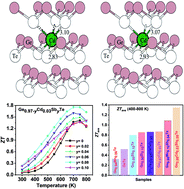
GeTe-based thermoelectric materials tend to be naturally heavily hole doped because of Ge lattice vacancies, and this complicates efforts to improve the figure of merit ZT. Herein, we report that partial substitution of Cd for Ge and doping with Sb can synergistically reduce the density of holes and improve the thermoelectric transport properties of GeTe. Density functional theory electronic structure calculations suggest that when Cd partially substitutes for Ge and forms CdxGe1−xTe, the energy offset between the light and heavy valence bands in both rhombohedral and cubic structures is reduced, promoting multi-band conduction that increases the hole carrier effective mass from 1.44m0 for pristine GeTe to 2.32m0 for Cd0.05Ge0.95Te. The ensuing valence band convergence enhances the Seebeck coefficient and yields a high power factor of 44.5 μW cm−1 K−2 at 800 K. Moreover, DFT calculations show a downward energy profile, indicating that as Cd enters the GeTe lattice it tends to move towards a hypothetical octahedral center to make six equal Cd–Te bonds. Such a local distortion in combination with the large mass and size difference between Ge and Cd strongly intensifies phonon scattering by point defects, lowering the lattice thermal conductivity in CdxGe1−xTe. Subsequent Sb doping in Cd0.03Ge0.97−ySbyTe reduces the inherent high carrier concentration in GeTe, leading to a remarkable enhancement of the Seebeck coefficient and the power factor over a wide temperature range. Furthermore, doping with Sb in Cd0.03Ge0.97−ySbyTe introduces additional point defect phonon scattering that results in an extremely low lattice thermal conductivity ∼ 0.71 W m−1 K−1 at 700 K for the Cd0.03Ge0.89Sb0.08Te sample. All those factors lead to a high thermoelectric figure of merit, ZT ∼ 1.8 at 700 K, and a high average ZT of 1.3 in the temperature interval of 400–800 K attained in Cd0.03Ge0.89Sb0.08Te.


1. Introduction

Thermoelectric (TE) conversion is a solid state electronic technology capable of capturing waste heat and converting it directly into useful electricity.1,2 The conversion efficiency of a thermoelectric (TE) material is defined by the dimensionless figure of merit ZT = σS2T/κ, where σ and S are the electrical conductivity and the Seebeck coefficient, respectively, κ is the total thermal conductivity, consisting of the electronic term κe and the lattice thermal conductivity contribution κlat, for the total thermal conductivity κ = κe + κlat, and T is the absolute temperature.3 Theoretical and experimental results have revealed that the electronic band engineering and the formation of an all scale hierarchical microstructure are the most effective routes for improving the thermoelectric properties, especially for group IV–VI compounds.4–12 To date, making use of synergistic approaches, a record high ZT ∼ 2.2–2.5 has been achieved in Na doped p-type PbTe–% EuTe/SrTe.13,14 Although the group 14 metal chalcogenides, such as PbQ and SnQ (Q = Se, Te) are some of the top thermoelectric materials, the germanium analogs are unique in their crystal structure and do not exhibit directly analogous thermoelectric properties. The reason for the structural difference is a strong tendency of the 4s2 lone pair of electrons in the Ge2+ ion to stereochemically expresses itself, thereby distorting the highly symmetric octahedral site in the typical rock-salt structure and thus lowering the local symmetry. Consequently, GeTe has the R3m crystallographic symmetry and Ge2+ has a trigonal pyramidal coordination environment with three short and three long Ge–Te bonds. The compound has a large number of Ge vacancies, which render the material heavily p-type. Therefore, the pristine GeTe possesses an inherently high hole carrier concentration (∼1020–1021 cm−3).15–17

When heated, GeTe undergoes a structural phase transition from the low-temperature rhombohedral structure to the high-temperature rock-salt cubic structure18–20 at a temperature around 700 K, maintaining a large number of intrinsic Ge vacancies in the low-temperature phase. Significant progress has been made in reducing the carrier concentration to the required optimum carrier concentration21,22 and enhancing the valence band degeneracy23,24 accompanied with a compelling improvement of the ZT value from 1.2 to above 2 in GeTe-based materials.22–37 In fact, in its high-temperature β-GeTe cubic crystal structure, GeTe exhibits similar electronic bands as its counterparts PbTe and SnTe, having a dominant higher-lying light energy band at L point and a lower-lying heavy energy band at Σ point. In contrast, the low-temperature rhombohedral structure also has similar two valence bands, but with a particular switch in energy band levels, where the energy of the light energy band at L point is lowered, making the heavy energy valence band Σ the dominant one in the carrier transport properties. Therefore, this understanding of the electronic band structure of GeTe in both rhombohedral and cubic structures suggests that engineering a band convergence might be a beneficial approach for enhancing the TE performance in GeTe.38–43

Previously, we have studied the effect of a magnetic impurity Mn2+ substituted on the site of Ge in GeTe. An ion of Mn2+ tends to form a strong rigid chemical bond with Te via sp3d2 orbitals. Such chemical bonding in Ge1−xMnxTe forces Mn atoms to sit in on-center positions of an octahedron formed by six atoms of Te via lengthening the short Ge–Te bond and shortening the longer Ge–Te bond to make them equal. This converts the original atomic arrangement into a cubic structure, and strongly suppresses the phase transition temperature. Moreover, substituting Ge by Mn2+ promotes the band convergence, which enhances the effective mass and, thus, the Seebeck coefficient. The presence of Mn also creates point defects, which lowers the lattice thermal conductivity.40

In this study, to test the band structure engineering approach in GeTe with a nonmagnetic element, we explore the role of Cd as an isovalent alloying element and Sb as an electron doping agent. We systematically investigate the effect of Cd doping on the crystal structure, electronic band structure, thermoelectric properties of CdxGe1−xTe, and then we optimize the carrier concentration in Ge1−xyCdxSbyTe (x = 0.03 and y = 0–0.10) by co-doping with Sb to further improve the thermoelectric performance. We show that introducing Cd in GeTe strongly modifies its electronic band structure by reducing the energy offset between the light and heavy valence bands in both low-temperature rhombohedral and high-temperature cubic structures, leading to an enhancement of the Seebeck coefficient and the power factor. Additionally, the large mass and size differences between the host atom and the Cd impurity, and the strong local structure distortion caused by the discordant nature of Cd in GeTe results in the very low lattice thermal conductivity that approaches the amorphous limit. Moreover, doping with Sb not only significantly reduces the carrier concentration of Cd0.03Ge0.97−ySbyTe to its optimal value, but it also further suppresses the thermal conductivity. A peak ZT value ∼1.8 at 700 K, and an extremely high average ZT of 1.3 over 400–800 K are achieved for Ge0.89Cd0.03Sb0.08Te, suggesting that the GeTe-based thermoelectric material is a robust candidate for power generation in the intermediate temperature range.

2. Experimental section

2.1 Synthesis

p-Type Ge1−xCdxTe (x = 0–0.10) and Ge0.97−yCd0.03SbyTe (y = 0–0.10) ingots were prepared by a simple conventional melting method. Constituent elements (Ge, Cd, Sb, and Te with 99.999% purity) in stoichiometric proportions were sealed in a quartz tube under vacuum and were heated in a rocking furnace to 1373 K, and were held at that temperature for 24 h. Subsequently, the sealed quartz tube was quenched in cold water, and then annealed at 873 K for 3 days. The obtained ingots were ground into fine powders, and vacuum sintered at 773 K under a pressure of 50 MPa applied for 5 min to obtain fully dense pellets by plasma activated sintering. The phase composition was characterized by powder X-ray diffraction (XRD, PRO-PANalytical Empyrean, Netherland) and Electron-Probe Microanalysis (EPMA, JXA-8230, JEOL, Japan) equipped with energy dispersive X-ray spectroscopy (EDS).

2.2 Sample characterization

The morphology of the prepared samples was analyzed by Transmission Electron Microscopy (TEM, JEM-2100F, JEOL, Japan). The electrical conductivity and the Seebeck coefficient were measured simultaneously by a standard four-probe method (ULVAC RIKO, ZEM-3, inc) in a helium atmosphere from 300 K to 800 K. Since the solubility limit of Cd in GeTe is about 0.05, and CdTe secondary phase is detected in samples with the Cd content above 0.06, we did not measure the electronic transport properties on samples above the solubility limit. The thermal conductivity was calculated from the measured thermal diffusivity D, specific heat capacity Cp, and the density d according to the relationship κ = D × Cp× d. The thermal diffusivity D was measured by the laser flash method (LFA-457, NETZSCH, Germany), the specific heat capacity Cp was calculated by the Dulong–Petit law, and the density of bulk samples was determined by the Archimedes method. Both electrical and thermal transport properties were measured along the pressing direction. The relative density of all pellets is about 98%. The low temperature (10–300 K) Hall coefficient (RH) and electrical conductivity (σ) were measured by a physical properties measurements system (PPMS-9, Quantum design, USA). The corresponding carrier concentration (n) and carrier mobility (μH) were calculated from the equations n = 1/(eRH) and μH = σ/ne, where e is the elementary charge.

2.3 Electronic band structure calculations

We used the density functional theory (DFT) to calculate the total energies and relaxed geometries of the GeTe and Ge1−xCdxTe structures. The DFT calculations were performed within the generalized gradient approximation (GGA) of Perdew–Burke–Ernzerhof for the exchange–correlation functional with projector augmented wave potentials.44 The periodic boundary conditions and a plane wave basis set were utilized as implemented in the Vienna ab initio simulation package (VASP).45 The total energies of the calculated systems were numerically converged to approximately 3 meV per cation using a basis set energy cutoff of 500 eV and dense k-point meshes corresponding to 4000 k-points per reciprocal atom in the Brillouin zone. We compute the energy profile of Cd atom relaxation from regular substituted Ge site using the nudged elastic band methods.46

3. Results and discussion

3.1 The role of Cd in Ge1−xCdxTe compounds

The XRD pattern for Ge1−xCdxTe (0 ≤ x ≤ 0.10) compounds is shown in Fig. 1(a). All samples can be indexed with the GeTe rhombohedral structure (space group R3m). Single phase compounds are observed for x ≤ 0.05, while for the samples with x ≥ 0.06, weak additional Bragg peaks are present at about 24° and 40°, indicating the formation of CdTe. The presence of the secondary phase as the content of Cd exceeds 0.05 suggests that the solubility limit of CdTe in CdxGe1−xTe is around 0.05. This is further supported by the x dependence of the lattice parameters shown in Fig. 1(b). The a-axis lattice parameter increases with the increasing Cd content and saturates when the Cd content is above 5%. The lattice expansion along the a-axis is consistent with the Vegard's law since the larger Cd2+ (0.95 Å) ion substitutes for the smaller Ge2+ (0.73 Å) ion. There is a slight decrease of the lattice parameter along the c-axis with the increase of Cd content. It should be noted that there is no remarkable decrease in the phase transition temperature of GeTe due to Cd doping, see Fig. S1 in the ESI. Using electron probe microanalysis (EPMA) and backscattering electron images (BSEI), it is clear that samples with x ≤ 0.05 show no CdTe precipitates, while samples with x equal 0.06 or higher contain the CdTe secondary phase, see white spots in Fig. 2, in agreement with XRD measurements in Fig. 1(a).
image file: c9ta10436d-f1.tif
Fig. 1 (a) Powder XRD patterns for Ge1−xCdxTe (x = 0–0.10) samples after SPS, (b) Rietveld refined lattice parameters as a function of the Cd content (x) at room temperature.

image file: c9ta10436d-f2.tif
Fig. 2 Electron probe microanalysis (EPMA) for Ge1−xCdxTe (x = 0, 0.03, 0.05 and 0.06) samples. Both secondary electron (SE) and back scattering electron (BSE) characterizations were performed on well-polished surfaces. The SE and BSE images show no impurity related to Cd for x ≤ 0.05, while samples with x ≥ 0.06 contain the CdTe secondary phase (white spot for x = 0.06 corresponding to CdTe are pointed out by arrows).

To probe the effect of Cd substitution in CdxGe1−xTe on the electronic band structure, the electronic bands of Ge27−xCdxTe27 (x = 0, 1, and 2) in both low-temperature rhombohedral and high-temperature cubic structures were calculated. The results show that dissolving Cd in GeTe leads to an effective band convergence, depicted in Fig. 3. Band structures of the low-temperature phase (rhombohedral structure, R3m space group) of pristine GeTe and of Cd-doped GeTe (Ge26CdTe27 and Ge25Cd2Te27) are shown in Fig. 3(a–c), respectively, while the band structures of high-temperature phase (cubic structure, Fm[3 with combining macron]m space group) of pristine GeTe and of Cd-doped GeTe (Ge26CdTe27 and Ge25Cd2Te27) are displayed in Fig. 3(d–f), respectively. In both cases, Ge 4p states dominate the bottom of the conduction bands, while Te 5p states play the major role at the top of the valence bands. For low temperature rhombohedral structure of Ge27−xCdxTe27, the energy offset between two top valence band are 0.15 eV, 0.09 eV and 0.08 eV for Ge27Te27, Ge26CdTe27, and Ge25Cd2Te27, respectively, while for high temperature cubic structure of Ge27−xCdxTe27, the energy offset between two top valence band are 0.21, 0.07 and 0.07 eV for Ge27Te27, Ge26CdTe27, and Ge25Cd2Te27, respectively. The theoretical calculations clearly suggest that dissolving Cd in GeTe decreases the energy difference between the light and heavy valence bands, and thus promoting the valence band convergence in both the rhombohedral and cubic phases.


image file: c9ta10436d-f3.tif
Fig. 3 Band structure for the Ge27−xCdxTe27 (x = 0, 1, 2) samples: (a–c) for low temperature rhombohedral structure of Ge27−xCdxTe27, the energy offset between two top valence band are 0.15 eV, 0.09 eV and 0.08 eV for Ge27Te27, Ge26CdTe27, and Ge25Cd2Te27, respectively. (d–f) For high temperature cubic structure of Ge27−xCdxTe27, the energy offset between two top valence band are 0.21, 0.07 and 0.07 eV for Ge27Te27, Ge26CdTe27, and Ge25Cd2Te27, respectively.

The temperature dependent electronic transport properties, including the electrical conductivity (σ), the Seebeck coefficient (S), and the power factor, are plotted in Fig. 4. The electrical conductivity for CdxGe1−xTe samples decreases with the greater Cd content and with the increasing temperature, behaving as a highly degenerate semiconductor. At room temperature, the electrical conductivity of pristine GeTe is 6704 S cm−1, while the electrical conductivity of the Cd0.05Ge0.95Te sample decreases to 3474 S cm−1. The temperature dependence of the Seebeck coefficient for all samples is shown in Fig. 4(b), and the Seebeck coefficients are positive, indicating that holes are the dominant charge carrier in CdxGe1−xTe. It is worth noting that the room temperature Seebeck coefficient increases from 31.6 μV K−1 for pristine GeTe to 52.4 μV K−1 for the Cd0.05Ge0.95Te sample. Additionally, with the rising temperature, the Seebeck coefficient climbs to higher values, from 158.4 μV K−1 for pristine GeTe to 173.8 μV K−1 for the Cd0.03Ge0.97Te sample at 750 K. The temperature dependent power factor is shown in Fig. 4(c). Significant enhancements in the power factor are observed with the increasing Cd content and temperature in our samples. The power factor increases from 38 μW cm−1 K−2 at 800 K for pristine GeTe to 48.6 μW cm−1 K−2 for x = 0.01, to 49.5 μW cm−1 K−2 for x = 0.02, and to 44.5 μW cm−1 K−2 for x = 0.03 samples. The power factor improvement is due to the large effective mass, which is enabled by the band convergence in Cd-doped CdxGe1−xTe. To demonstrate this convincingly, the effective mass (m*) was estimated based on a single parabolic band approximation (SPB)40,47 and the results are shown in Table 1. Specifically, the effective mass increases from 1.44m0 for pristine GeTe to 2.32m0 for the sample with x = 0.05. The correlation between the room temperature Hall carrier concentration and the Seebeck coefficient (Pisarenko plot) with a comparison of the data from the previous publications is plotted in Fig. 5(a). The Seebeck coefficient deviates from the values predicted by the two-valence band model.24,31 The higher Seebeck coefficient in Cd-doped GeTe than the theoretical Pisarenko line predicts reveal significantly enhanced effective mass. Meanwhile, it should be also noted that the presence of Cd in GeTe slightly decreases the carrier concentration. It is well known that the high carrier concentration in GeTe is ascribed to the high concentration of Ge vacancies. Additionally, Cd is isovalent to Ge in GeTe, meaning that Cd in the GeTe matrix may not significantly change the carrier concentration, as would be the case in aliovalent alloying. However, a slight decrease observed in the carrier concentration of Ge1−xCdxTe compounds may indicate that Cd decreases the concentration of Ge vacancies in the GeTe structure. This is confirmed by the constituency ratio calculated from the EPMA data analysis, as shown in Fig. 5(b). The ratio between a cation (Cd and Ge) and an anion (Te) increases with the increasing content of Cd, and is accompanied by a slight decrease in the carrier concentration, indicating a decrease in the concentration of Ge vacancies.


image file: c9ta10436d-f4.tif
Fig. 4 Electronic transport properties as a function of temperature for Ge1−xCdxTe (x = 0–0.05) samples: (a) electrical conductivity, (b) Seebeck coefficient, (c) power factor.
Table 1 Room temperature transport properties of Ge1−xCdxTe (x = 0–0.05)
Samples σ (S cm−1) S (μV K−1) η F (eV) n (1020 cm−3) μ H (cm2 V−1 s−1) m*/m0
x = 0 6704 31.6 8.98 9.02 50.97 1.44
x = 0.01 6311 41.47 6.82 8.13 52.69 1.76
x = 0.02 5325 44.98 6.28 6.10 61.0 1.58
x = 0.03 4532 47.86 5.89 8.43 34.73 2.08
x = 0.04 4132 48.83 5.77 7.90 33.85 2.04
x = 0.05 3474 52.41 5.35 8.65 29.35 2.32


image file: c9ta10436d-f5.tif
Fig. 5 (a) The correlation between the room temperature Hall carrier concentration and the Seebeck coefficient (Pisarenko plot) together with the data from previous works: Ge1−xSbxTe23 and Ge1−xyCdxBiyTe,42 for comparison. The black line in the figure shows the Pisarenko plot with two band model. (b) The constituency ratio from the electron probe microanalysis data and the carrier concentration at different Cd contents. The increasing ratio between the cation (Cd and Ge) and the anion (Te) with the rising Cd content indicates a decrease in the concentration of Ge vacancies.

The temperature dependent total thermal conductivity data are shown in Fig. 6(a). The thermal conductivity is remarkably reduced upon Cd alloying. The pristine GeTe sample shows a slightly higher total thermal conductivity value of 8.80 W m−1 K−1 at 300 K, which falls to 5.43 W m−1 K−1 for the x = 0.03 sample at room temperature. The thermal conductivity decreases with the increasing temperature from 2.79 W m−1 K−1 for pristine GeTe at 750 K to 2.39 W m−1 K−1 for x = 0.03 at the same temperature. The lattice thermal conductivity κlat, shown in Fig. 6(b), is obtained by subtracting the electronic thermal conductivity κe from the total thermal conductivity κ, κlat = κκe. Here, the electronic thermal conductivity is calculated from the Wiedemann–Franz law, κe = LσT, where L is the Lorenz number, σ is the measured electrical conductivity, and T is the absolute temperature. The lattice thermal conductivity decreases from 3.58 W m−1 K−1 for pristine GeTe to 2.25 W m−1 K−1 for the Cd0.03Ge0.97Te sample at room temperature, representing some 70% reduction. The κlat is further decreased as the temperature increases, reaching 0.61 W m−1 K−1 at 750 K for Cd0.03Ge0.97Te, which is obviously lower compared to 0.90 W m−1 K−1 for pristine GeTe, and is close to the amorphous limit value (0.5 W m−1 K−1) estimated by the model of Cahill.48


image file: c9ta10436d-f6.tif
Fig. 6 Thermal transport properties as a function of temperature for Ge1−xCdxTe (x = 0–0.05) samples. (a) Total thermal conductivity, (b) lattice thermal conductivity, and (c) figure of merit ZT as a function of temperature for Ge1−xCdxTe (x = 0–0.05) samples.

The lattice thermal conductivity is strongly depressed even though the fraction of Cd dissolved in GeTe is only 3%. It is difficult to rationalize that such a small amount of Cd could fully account for the very large drop observed in κlat (even taking into account large differences in the atomic mass and size), and it is likely that a new mechanism of strong phonon scattering is at play. We propose that such new mechanism derives from the discordant nature of Cd atom in the GeTe lattice, which has also been invoked as an effective approach for reducing the lattice thermal conductivity in other thermoelectric materials.49,50

To understand this mechanism and its effect on the significant decrease of lattice thermal conductivity due to Cd doping, we examine the local environment of Cd atom in the GeTe. Based on the DFT calculations, as Cd substitutes Ge, the Cd atom finds it energetically unfavorable to occupy a trigonal pyramidal site and prefers to move towards the center of the octahedron to make six Ge/Cd–Te bonds in the octahedral structural unit nearly equal. Fig. 7(a and b) show the Cd substitution positions in GeTe before and after relaxation. Initially, Ge locates on the regular Ge site in the rhombohedral GeTe lattice, makes short and long Ge–Te bonds of 2.83 Å and 3.10 Å, respectively, see Fig. 7(a). After relaxation, Cd atom shifts the position towards the hypothetical octahedral center to make six bonds with the nearby Te atoms, leading to a slight increase in the Cd–Te short bond, as shown in Fig. 7(b). The energy profile of Cd atom relaxation from regular substituted Ge site to the hypothetical octahedral center has been investigated by the nudged elastic band methods.46 As can be seen from Fig. 7(c), the shifted Cd atom is much more favorable than the regular substitution by about 170 meV. And there is a very flat energy landscape for Cd atom further shifting to the octahedral site. It is known in our previous example, the discordant Ge dopant in PbSe50 leads to a significant lattice thermal conductivity suppressing because of Ge which softened the optical modes and induced strong local strain fields. Similar to the case of Ge in PbSe, the Cd atom in GeTe also induces a strong local strain and it is believed to introduce additional phonon scattering for lowering lattice thermal conductivity.


image file: c9ta10436d-f7.tif
Fig. 7 (a) The atoms position in the initial pristine GeTe and (b) the final position of Cd substituted for Ge in the R3m structure. (c) Calculated total energy profile of Ge26CdTe27 with Cd located at various positions between the octahedral and tetrahedral sites. The downward energy profile shows that Cd is sliding down and moving to the hypothetical octahedral center with six Te atoms around it.

The measured room temperature sound velocities of the Ge1−xCdxTe samples, shown in Fig. S2, are substantially immune to the presence of Cd, suggesting that phonon softening could not be the cause of the lower lattice thermal conductivity in Ge1−xCdxTe.21,39,42,51

We calculated the impurity phonon scattering parameters using eqn (S1)–(S7) in the ESI, based on the model by Callaway.52 The scattering parameters for the Ge1−xCdxTe compounds (Table 2 and Fig. S2b) were found to increase with the increasing Cd content, suggesting that the lattice thermal conductivity is strongly reduced due to the point defect disorder scattering. The discordant nature of the Cd atom is reflected in the higher value for ΓS, which represents the unusually large strain field fluctuations in the structure.

Table 2 Disorder scattering parameters ΓM, ΓS, and Γ, strain field related adjustable parameter ε1, disorder scaling parameter u, and lattice thermal conductivity of Ge1−xCdxTe (x = 0–0.05)
Samples Γ M (10−3) Γ S (10−3) Γ (10−3) ε 1 u κ L (W m−1 K−1)
x = 0 3.58
x = 0.01 0.78 34.76 35.54 468 1.43 3.01
x = 0.02 1.54 36.99 38.53 253 1.49 2.69
x = 0.03 2.27 63.71 65.98 292 1.95 2.51
x = 0.04 2.98 56.11 59.10 196 1.85 2.27
x = 0.05 3.68 61.27 64.95 173 1.94 2.25


The dimensionless figure of merit ZT for the Ge1−xCdxTe samples as a function of temperature is shown in Fig. 6(c). A peak ZT value ∼1.4 at 750 K is obtained as a result of the high power factor combined with the low lattice thermal conductivity in Ge1−xCdxTe.

3.2 Counter doping of Ge1−xCdxTe with Sb

The above discussion show that the presence of Cd in GeTe not only promotes the valence band convergence, boosting the electronic properties, but it also creates a strong lattice distortion, which intensifies phonon scattering and drastically suppresses the thermal conductivity. It should be noted that Cd is isovalent with Ge in Ge1−xCdxTe and the carrier concentration in the Ge1−xCdxTe compounds is not at its optimal value required for the high thermoelectric performance. To optimize the carrier concentration in the Ge1−xCdxTe samples, we have chosen the Ge0.97Cd0.03Te alloy composition and Sb as an electron donor dopant aiming to reduce the carrier concentration of holes. We used a series of Sb doping levels y and synthesized Ge0.97−yCd0.03SbyTe compounds for 0 ≤ y ≤ 0.1.

The powder X-ray diffraction patterns of the Ge0.97−yCd0.03SbyTe samples are shown in Fig. 8(a). All samples appear to have a single phase rhombohedral structure of GeTe (R3m) for y < 0.10. However, in a sample with the Sb content of 0.10, the characteristic double-peak structure merges into a single broad peak, indicating a conversion into the cubic rock salt structure (Fm[3 with combining macron]m). A similar phenomenon has been observed in SbxGe1−xTe23 compounds and MnxGe1−xTe.40 Doping or forming a solid solution can modify the octahedral structural unit by lengthening the short Ge–Te bond and shortening the longer Ge–Te bond, making them equal, and converting the rhombohedral structure into a cubic one, as demonstrated in the case of Mn-doped GeTe.40 In our case, as the concentration of Sb increases, the lattice parameter along the a-axis increases, while it decreases along the c-axis, in accord with the X-ray diffraction patterns in Fig. 8(a).


image file: c9ta10436d-f8.tif
Fig. 8 (a) Powder XRD patterns for Ge0.97−yCd0.03SbyTe (y = 0–0.10) samples after SPS. (b) Rietveld refined lattice parameters as a function of the Sb content (y) at room temperature.

Fig. 9 shows TEM images for Ge0.89Cd0.03Sb0.08Te as the representative sample. Fig. 9(a) depicts bright field TEM image showing domain variants with bright and dark contrast, which is commonly referred to as a herringbone structure in GeTe.53–55Fig. 9(b) displays an HRTEM image with the interplanar distance d = 0.34 nm, which belongs to (021) planes of the GeTe rhombohedral structure. The inset in Fig. 9(b) shows the Fast Fourier Transformed (FFTs) diffraction pattern, where no spot splitting is discernible along the (001) zone axis, suggesting the sample is already in a pseudo-cubic crystalline structure. Fig. 9(c and d) show another bright TEM image representing domain variants with different polarities in a sharp turn herringbone structure. Throughout the sample, there exist several twin domain boundaries with different herringbone patterns that can scatter long-wavelength phonons. Fig. 9(e) shows a STEM image of the Ge0.089Cd0.03Sb0.08Te sample. The herringbone structures in the sample are clearly observed, and the chemical composition analyzed by EDS mapping and shown in Fig. 9(f) indicates homogeneously distributed elements with no phase segregation.


image file: c9ta10436d-f9.tif
Fig. 9 (a) Low magnification TEM image of the Ge0.089Cd0.03Sb0.08Te sample with the herringbone structure. (b) HRTEM image for (a). (c) TEM images for the Ge0.089Cd0.03Sb0.08Te sample with different domain variants. (d) HRTEM for (c). (e) STEM image and (f) elements distribution by EDS mapping in the Ge0.089Cd0.03Sb0.08Te sample.

The transport properties of the Ge0.97−yCd0.03SbyTe samples are measured from room temperature to 800 K, see Fig. 10. Fig. 10(a) shows the temperature-dependent electrical conductivity of Ge0.97−yCd0.03SbyTe compounds. The electrical conductivity decreases from 4531.9 S cm−1 for Ge0.97Cd0.03Te to 421.8 S cm−1 for the Ge0.87Cd0.03Sb0.10Te sample at room temperature. Furthermore, the high-temperature electrical conductivity decreases drastically with the increasing temperature, and the structure is referred to as a highly degenerate semiconductor. The temperature-dependent Seebeck coefficient for the Ge0.97−yCd0.03SbyTe samples increases with the increasing Sb content and temperature, see Fig. 10(b). Positive values for the Seebeck coefficient are consistent with Hall carrier concentration measurements summarized in Table 3, which indicates a p-type conduction in Ge0.97−yCd0.03SbyTe. The decrease in the reduced Fermi level, Table 3, suggests that the Fermi level moves upward from the valence band, accompanied with a reduced carrier concentration. The temperature-dependent power factor (PF) is shown in Fig. 10(c). The overall PF increases with both the Sb content and temperature, and great enhancements are achieved at lower temperatures, where at 500 K the highest PF value of 32.7 μW m−1 K−2 is achieved for Ge0.89Cd0.03Sb0.08Te compared to 24.4 μW m−1 K−2 measured for Ge0.97Cd0.03Te. For comparison, the thermoelectric properties of Sb doped GeTe (Ge1−ySbyTe) are also given in Fig. S3 (ESI).


image file: c9ta10436d-f10.tif
Fig. 10 Electronic transport properties as a function of temperature for Ge0.97−yCd0.03SbyTe (y = 0–0.10) samples: (a) electrical conductivity and (b) Seebeck coefficient. The increasing and decreasing trends in the electrical conductivity and the Seebeck coefficient at high temperatures indicate the presence of bipolar conduction. (c) Power factor as a function of temperature for Ge0.97−yCd0.03SbyTe (y = 0–0.10) samples, showing a large enhancement at temperatures below 600 K with respect to the sample with no Sb doping.
Table 3 Room temperature transport properties of Ge0.97−yCd0.03SbyTe (y = 0–0.10)
Samples σ (S cm−1) S (μV K−1) η F (eV) n (1020 cm−3) μ H (cm2 V−1 s−1) m*/m0
y = 0 4532 47.9 5.89 8.43 34.7 2.08
y = 0.02 3212 59.2 4.69 5.37 38.0 1.91
y = 0.04 2548 66.5 4.13 4.35 35.1 1.86
y = 0.06 1829 81.8 3.21 3.37 35.3 1.93
y = 0.08 1249 111.3 2.04 3.02 22.6 2.44
y = 0.10 422 168.3 0.65 2.28 10.4 3.07


The temperature-dependent carrier concentration and the carrier mobility in the 10–300 K temperature range are shown in Fig. 11(a and b), respectively. The carrier concentration is markedly reduced in the entire temperature range upon doping with Sb, which weakens carrier–carrier scattering. However, doping with Sb also intensifies point defect scattering, and, overall, the carrier mobility decreases with the greater content of Sb and the rising temperature, Fig. 11(b). The carrier mobility decreases distinctly following the T−1/2 trend, suggesting the predominant alloy scattering mechanism.39


image file: c9ta10436d-f11.tif
Fig. 11 (a) Low temperature carrier concentration and (b) Hall carrier mobility of Ge0.97−yCd0.03SbyTe (y = 0–0.10) samples derived from Hall effect measurements in the temperature interval 10–300 K.

Fig. 12(a) shows the temperature-dependent total thermal conductivity for Ge0.97−yCd0.03SbyTe samples. A remarkable reduction in the total thermal conductivity is achieved in Sb-doped Ge0.97Cd0.03Te compounds. At room temperature, the κtotal for Ge0.97Cd0.03Te is 5.4 W m−1 K−1, whereas for Ge0.87Cd0.03Sb0.10Te it is only 1.6 W m−1 K−1. The lattice thermal conductivity κlat, shown in Fig. 12(b), is obtained by subtracting the electronic thermal conductivity κe from the total thermal conductivity κtotal, with the calculated κe shown in Fig. S4(a), ESI. The Lorenz number, Fig. S4(b), is calculated using the reduced Fermi energy derived from the Seebeck coefficient measurement assuming the validity of a single parabolic band model. The κlat decreases with the increasing Sb content and temperature. The lowest value of κlat = 1.30 W m−1 K−1 is achieved for the Ge0.89Cd0.03Sb0.08Te sample at room temperature, and the value is further reduced to 0.71 W m−1 K−1 at 700 K. The lower lattice thermal conductivity in the Ge0.097−yCd0.03SbyTe samples may be attributed to the higher density of point defects that originate from the presence of Sb. Interestingly, although Sb doping introduces additional point defects, the high temperature lattice thermal conductivity values in Ge0.097−yCd0.03SbyTe are slightly higher than those in the undoped Ge0.89Cd0.03Te sample. This may be due to the reduced phonon-vacancy scattering upon an introduction of Sb electron donors. Fig. 13(a) shows the temperature-dependent figure of merit ZT for the Ge0.097−yCd0.03SbyTe samples. The highest ZT value of ∼1.8 at 700 K is exhibited by the Ge0.89Cd0.03Sb0.08Te sample, resulting from the reduced thermal conductivity due to strong point defects scattering of phonons introduced by Sb doping.


image file: c9ta10436d-f12.tif
Fig. 12 Thermal transport properties as a function of temperature for Ge1−yCd0.03SbyTe (y = 0–0.10) samples: (a) total thermal conductivity and (b) lattice thermal conductivity.

image file: c9ta10436d-f13.tif
Fig. 13 (a) Figure of merit ZT as a function of temperature for Ge1−yCd0.03SbyTe (y = 0–0.10) samples and (b) the average thermoelectric figure of merit of Ge0.89Cd0.03Sb0.08Te compared with other selected GeTe-based materials, and showing the conversion efficiency of GeTe-based structures.

From the point of view of a practical device, it is the average ZT (ZTave) value, which determines the conversion efficiency of a thermoelectric module intended to operate over a wide range of temperatures. The calculated average ZT in the temperature interval of 400–800 K is shown in Fig. 13(b), and the corresponding data for other related materials are also plotted for comparison. The obtained ZTave ∼ 1.3 in the 400–800 K temperature range is among the highest reported in GeTe-based thermoelectric materials.

4. Conclusions

In this study, we have improved the thermoelectric properties of GeTe through a synergistic effect of band convergence via Cd partially substituting for Ge in GeTe, and optimizing the carrier concentration by Sb doping. Cd in the CdxGe1−xTe compounds effectively alters the electronic band structure of GeTe by reducing the energy offset between the light and heavy valence bands in both rhombohedral and cubic structures, thereby increasing the effective masses, which results in a significant enhancement of the electronic transport properties. Moreover, the local structural distortion created by Cd atom was documented as the Cd atom likely moves towards the hypothetical octahedral center to establish six bonds with the neighboring Te atoms. The density functional theory (DFT) calculations show a downward energy profile, indicating that Cd is sliding down to the octahedral center with six Te atoms around it. This distortion strongly reinforces phonon scattering, resulting in a greatly reduced lattice thermal conductivity that reaches values as low as 0.61 W m−1 K−1 at 700 K in Ge0.97Cd0.03Te. Furthermore, doping Ge0.97Cd0.03Te with Sb to form Ge0.97−yCd0.03SbyTe significantly reduces the carrier concentration to the required optimal carrier concentration of 2.80 × 1020 cm−3, resulting in the enhanced power factor of 36 μW m−1 K−2 at 700 K for the Ge0.89Cd0.03Sb0.08Te sample. At the same time, the strengthened point defect phonon scattering further reduces the total thermal conductivity. Consequently, high ZT values reaching 1.8 at 700 K, and the high average ZT of 1.3 in the temperature interval of 400–800 K are obtained for Ge0.89Cd0.03Sb0.08Te sample, which is among the top values in GeTe-based compounds.

Conflicts of interest

The authors declare no conflict of interest.

Acknowledgements

The authors thank Rong Jiang, Tingting Luo and Meijun Yang for help with the HRTEM analysis and EPMA measurement. The authors wish to acknowledge support from the National Key Research and Development Program of China (Grant No. 2018YFB0703600) and the Natural Science Foundation of China (51972256, 51872219, 51632006, and 51521001).

References

  1. C. Yu and K. Chau, Energy Convers. Manage., 2009, 50, 1506–1512 CrossRef CAS.
  2. Z. Tang, Y. Deng, C. Su, W. Shuai and C. Xie, Case Studies in Thermal Engineering, 2015, 5, 143–150 CrossRef.
  3. G. J. Snyder and E. S. Toberer, Nat. Mater., 2008, 7, 105 CrossRef CAS PubMed.
  4. G. Tan, L. D. Zhao, F. Shi, J. W. Doak, S. H. Lo, H. Sun, C. Wolverton, V. P. Dravid, C. Uher and M. G. Kanatzidis, J. Am. Chem. Soc., 2014, 136, 7006–7017 CrossRef CAS PubMed.
  5. W. Liu, X. Tan, K. Yin, H. Liu, X. Tang, J. Shi, Q. Zhang and C. Uher, Phys. Rev. Lett., 2012, 108, 166601 CrossRef PubMed.
  6. K. Biswas, J. He, I. D. Blum, C.-I. Wu, T. P. Hogan, D. N. Seidman, V. P. Dravid and M. G. Kanatzidis, Nature, 2012, 489, 414 CrossRef CAS PubMed.
  7. M. Ohta, K. Biswas, S. H. Lo, J. He, D. Y. Chung, V. P. Dravid and M. G. Kanatzidis, Adv. Energy Mater., 2012, 2, 1117–1123 CrossRef CAS.
  8. Y. Xiao, H. Wu, J. Cui, D. Wang, L. Fu, Y. Zhang, Y. Chen, J. He, S. J. Pennycook and L.-D. Zhao, Energy Environ. Sci., 2018, 11, 2486–2495 RSC.
  9. Y. Pei, Z. M. Gibbs, A. Gloskovskii, B. Balke, W. G. Zeier and G. J. Snyder, Adv. Energy Mater., 2014, 4, 1400486 CrossRef.
  10. Z. Z. Luo, X. Zhang, X. Hua, G. Tan, T. P. Bailey, J. Xu, C. Uher, C. Wolverton, V. P. Dravid and Q. Yan, Adv. Funct. Mater., 2018, 28, 1801617 CrossRef.
  11. G. Zheng, X. Su, H. Xie, Y. Shu, T. Liang, X. She, W. Liu, Y. Yan, Q. Zhang and C. Uher, Energy Environ. Sci., 2017, 10, 2638–2652 RSC.
  12. G. Tan, F. Shi, S. Hao, H. Chi, T. P. Bailey, L. D. Zhao, C. Uher, C. Wolverton, V. P. Dravid and M. G. Kanatzidis, J. Am. Chem. Soc., 2015, 137, 11507–11516 CrossRef CAS PubMed.
  13. Z. Chen, Z. Jian, W. Li, Y. Chang, B. Ge, R. Hanus, J. Yang, Y. Chen, M. Huang and G. J. Snyder, Adv. Mater., 2017, 29, 1606768 CrossRef PubMed.
  14. G. Tan, F. Shi, S. Hao, L.-D. Zhao, H. Chi, X. Zhang, C. Uher, C. Wolverton, V. P. Dravid and M. G. Kanatzidis, Nat. Commun., 2016, 7, 12167 CrossRef CAS PubMed.
  15. A. H. Edwards, A. C. Pineda, P. A. Schultz, M. G. Martin, A. P. Thompson, H. P. Hjalmarson and C. J. Umrigar, Phys. Rev. B: Condens. Matter Mater. Phys., 2006, 73, 045210 CrossRef.
  16. D. Freik, I. Gorichok and L. Yurchyshyn, Chem. Met. Alloys, 2012, 5, 155–159 Search PubMed.
  17. J. Lewis, Phys. Status Solidi B, 1969, 35, 737–745 CrossRef CAS.
  18. K. Rabe and J. Joannopoulos, Phys. Rev. B: Condens. Matter Mater. Phys., 1987, 36, 3319 CrossRef CAS PubMed.
  19. W. Johnston and D. Sestrich, J. Inorg. Nucl. Chem., 1961, 19, 229–236 CrossRef CAS.
  20. A. Lebedev, I. Sluchinskaya, V. Demin and I. Munro, Phase Transitions: A Multinational Journal, 1997, 60, 67–77 CrossRef CAS.
  21. Z. Bu, W. Li, J. Li, X. Zhang, J. Mao, Y. Chen and Y. Pei, Mater. Today Phys., 2019, 9, 100096 CrossRef.
  22. D. Wu, L.-D. Zhao, S. Hao, Q. Jiang, F. Zheng, J. W. Doak, H. Wu, H. Chi, Y. Gelbstein and C. Uher, J. Am. Chem. Soc., 2014, 136, 11412–11419 CrossRef CAS PubMed.
  23. S. Perumal, S. Roychowdhury, D. S. Negi, R. Datta and K. Biswas, Chem. Mater., 2015, 27, 7171–7178 CrossRef CAS.
  24. J. Li, X. Zhang, S. Lin, Z. Chen and Y. Pei, Chem. Mater., 2016, 29, 605–611 CrossRef.
  25. K. Saheb Bayikadi, S. Raman, C. T. Wu, C. Xia, Y. Chen, L. Chen, K. H. Chen and F.-C. Chou, J. Mater. Chem. A, 2019, 7, 15181 RSC.
  26. H. Sun, X. Lu, H. Chi, D. T. Morelli and C. Uher, Phys. Chem. Chem. Phys., 2014, 16, 15570–15575 RSC.
  27. E. Hazan, N. Madar, M. Parag, V. Casian, O. Ben-Yehuda and Y. Gelbstein, Adv. Electron. Mater., 2015, 1, 1500228 CrossRef.
  28. S. Perumal, S. Roychowdhury and K. Biswas, Inorg. Chem. Front., 2016, 3, 125–132 RSC.
  29. J. Li, H. Wu, D. Wu, C. Wang, Z. Zhang, Y. Li, F. Liu, W.-q. Ao and J. He, Chem. Mater., 2016, 28, 6367–6373 CrossRef CAS.
  30. N. Madar, T. Givon, D. Mogilyansky and Y. Gelbstein, J. Appl. Phys., 2016, 120, 035102 CrossRef.
  31. X. Zhang, J. Li, X. Wang, Z. Chen, J. Mao, Y. Chen and Y. Pei, J. Am. Chem. Soc., 2018, 140, 15883–15888 CrossRef CAS PubMed.
  32. J. Li, X. Zhang, X. Wang, Z. Bu, L. Zheng, B. Zhou, F. Xiong, Y. Chen and Y. Pei, J. Am. Chem. Soc., 2018, 140, 16190–16197 CrossRef CAS PubMed.
  33. D. Wu, L. Xie, X. Xu and J. He, Adv. Funct. Mater., 2019, 29, 1806613 CrossRef.
  34. J. Dong, F.-H. Sun, H. Tang, J. Pei, H.-L. Zhuang, H.-H. Hu, B.-P. Zhang, Y. Pan and J.-F. Li, Energy Environ. Sci., 2019, 12, 1396–1403 RSC.
  35. J. Li, Y. Xie, C. Zhang, K. Ma, F. Liu, W. Ao, Y. Li and C. Zhang, ACS Appl. Mater. Interfaces, 2019, 11, 20064–20074 CrossRef CAS PubMed.
  36. P.-C. Wei, C.-X. Cai, C.-R. Hsing, C.-M. Wei, S.-H. Yu, H.-J. Wu, C.-L. Chen, D.-H. Wei, D.-L. Nguyen and M. M. Chou, Sci. Rep., 2019, 9, 8616 CrossRef PubMed.
  37. S. Perumal, M. Samanta, T. Ghosh, U. S. Shenoy, A. K. Bohra, S. Bhattacharya, A. Singh, U. V. Waghmare and K. Biswas, Joule, 2019, 3, 2565–2580 CrossRef CAS.
  38. J. Li, Z. Chen, X. Zhang, Y. Sun, J. Yang and Y. Pei, NPG Asia Mater., 2017, 9, e353 CrossRef CAS.
  39. M. Hong, Y. Wang, W. Liu, S. Matsumura, H. Wang, J. Zou and Z. G. Chen, Adv. Energy Mater., 2018, 8, 1801837 CrossRef.
  40. Z. Zheng, X. Su, R. Deng, C. Stoumpos, H. Xie, W. Liu, Y. Yan, S. Hao, C. Uher and C. Wolverton, J. Am. Chem. Soc., 2018, 140, 2673–2686 CrossRef CAS PubMed.
  41. Z. Liu, J. Sun, J. Mao, H. Zhu, W. Ren, J. Zhou, Z. Wang, D. J. Singh, J. Sui and C.-W. Chu, Proc. Natl. Acad. Sci. U. S. A., 2018, 115, 5332–5337 CrossRef CAS PubMed.
  42. J. Li, W. Li, Z. Bu, X. Wang, B. Gao, F. Xiong, Y. Chen and Y. Pei, ACS Appl. Mater. Interfaces, 2018, 10, 39904–39911 CrossRef CAS PubMed.
  43. M. Hong, Y. Wang, T. Feng, Q. Sun, S. Xu, S. Matsumura, S. T. Pantelides, J. Zou and Z.-G. Chen, J. Am. Chem. Soc., 2018, 141, 1742–1748 CrossRef PubMed.
  44. P. E. Blöchl, Phys. Rev. B: Condens. Matter Mater. Phys., 1994, 50, 17953 CrossRef PubMed.
  45. G. Kresse and J. Furthmüller, Phys. Rev. B: Condens. Matter Mater. Phys., 1996, 54, 11169 CrossRef CAS PubMed.
  46. G. Henkelman, B. P. Uberuaga and H. Jónsson, J. Chem. Phys., 2000, 113, 9901–9904 CrossRef CAS.
  47. E. Nshimyimana, X. Su, H. Xie, W. Liu, R. Deng, T. Luo, Y. Yan and X. Tang, Sci. Bull., 2018, 63, 717–725 CrossRef CAS.
  48. D. G. Cahill, S. K. Watson and R. O. Pohl, Phys. Rev. B: Condens. Matter Mater. Phys., 1992, 46, 6131 CrossRef CAS PubMed.
  49. J. M. Hodges, S. Hao, J. A. Grovogui, X. Zhang, T. P. Bailey, X. Li, Z. Gan, Y.-Y. Hu, C. Uher and V. P. Dravid, J. Am. Chem. Soc., 2018, 140, 18115–18123 CrossRef CAS PubMed.
  50. Z.-Z. Luo, S. Hao, X. Zhang, X. Hua, S. Cai, G. Tan, T. P. Bailey, R. Ma, C. Uher and C. Wolverton, Energy Environ. Sci., 2018, 11, 3220–3230 RSC.
  51. S. Roychowdhury, M. Samanta, S. Perumal and K. Biswas, Chem. Mater., 2018, 30, 5799–5813 CrossRef CAS.
  52. J. Callaway and H. C. von Baeyer, Phys. Rev., 1960, 120, 1149 CrossRef CAS.
  53. M. Snykers, P. Delavignette and S. Amelinckx, Mater. Res. Bull., 1972, 7, 831–839 CrossRef CAS.
  54. H. S. Lee, B.-S. Kim, C.-W. Cho, M.-W. Oh, B.-K. Min, S.-D. Park and H.-W. Lee, Acta Mater., 2015, 91, 83–90 CrossRef CAS.
  55. P. A. Vermeulen, A. Kumar, G. H. ten Brink, G. R. Blake and B. J. Kooi, Cryst. Growth Des., 2016, 16, 5915–5922 CrossRef CAS.

Footnote

Electronic supplementary information (ESI) available. See DOI: 10.1039/c9ta10436d

This journal is © The Royal Society of Chemistry 2020