
Crystallization kinetics of rapid spray plasma processed multiple cation perovskites in open air†
Michael Q.
Hovish
a,
Nicholas
Rolston
b,
Karsten
Brüning
 c,
Florian
Hilt
a,
Christopher
Tassone
c and
Reinhold H.
Dauskardt
*a
c,
Florian
Hilt
a,
Christopher
Tassone
c and
Reinhold H.
Dauskardt
*a
aDepartment of Materials Science and Engineering, Stanford University, Stanford, CA 94305-2205, USA. E-mail: dauskardt@stanford.edu; Fax: +1 650 725 4034; Tel: +1 650 725 0679
bDepartment of Applied Physics, Stanford University, Stanford, CA, USA
cStanford Synchrotron Radiation Lightsource, SLAC National Accelerator Laboratory, Menlo Park, CA, USA
First published on 26th November 2019
Abstract
Rapid Spray Plasma Processing (RSPP) is a high throughput, scalable, and open-air route toward manufacturing perovskite solar modules. The plasma exposure is dosed such that the perovskite precursor solution is cured in milliseconds using a combination of rapid heating, reactive species, and UV photons. We implemented in situ wide angle X-ray scattering (WAXS) to characterize the crystal growth in multiple cation, mixed halide perovskite thin films—Csx(MAzFA1−z)1−xPb(Br0.17I0.83)3 for 0.05 ≤ x ≤ 0.25—fabricated in open air. The use of synchrotron radiation and high detector speeds resolved the formation and dissolution of a transient intermediate crystalline phase during the tens of milliseconds when the perovskite crystallized. Increasing the mole fraction of cesium and methylammonium resulted in a decrease in the intermediate phase and an increase in the average grain diameter. Increasing the cesium fraction suppressed phase segregation, as observed in photoluminescence. Calculations showed the refractive index decreased and the extinction coefficient increased with cesium fraction. Based on the rapid crystallization kinetics, RSPP perovskite films exhibit residual stress values >5× lower than spin coated films. Understanding the kinetics of perovskite formation enables the design of perovskite films with improved thermomechanical and operational stability.
Introduction
Perovskite solar cells (PSCs) with power conversion efficiency (PCE) values in excess of 22% contend with silicon photovoltaics based on device performance.1 Efficiency aside, however, PSC stability is hindered from environmental stressors that result in light,2 thermal,3,4 and moisture-induced5 decomposition. Another critical stability limitation is the intrinsic thermomechanical fragility of the perovskite layer.6 It was recently shown that perovskites have a large coefficient of thermal expansion7,8 (CTE) relative to glass substrates, which leads to large residual tensile stresses.9–11 Temperatures at or above 100 °C are typically employed during conventional film growth,3 causing both the substrate and the film to expand. The perovskite crystallizes and bonds to the substrate, a constraint which prevents the film from shrinking an equilibrium distance upon cooling. This mismatch induces tensile stress, which drives failure12 and can accelerate degradation under operational conditions.10,11 In particular, film stress has been shown to accelerate the rate of photochemical degradation in many materials—such as fuel cell membranes,13 laser diodes,14 and encapsulants15—and recent studies have shown that perovskite stability is also affected by tensile stress.10,11Recently, we reported a new scalable method, Rapid Spray Plasma Processing (RSPP), to crystallize high quality metal halide perovskite thin films in open air and on the millisecond timescale.16 RSPP PSCs displayed good power conversion efficiencies (>15%), high open-circuit voltages (>1.05 V), and the highest reported fracture toughness (4.4 J m−2) for planar perovskite films without additional reinforcing scaffolds.17 The rapid cure is enabled by an open air plasma device—which conveys energy to an ultrasonically sprayed solution of perovskite precursors—and has been used to produce conductive metal oxides18,19 along with inorganic barrier films.20 The plasma exposure is typically several hundred milliseconds, during which the convection of thermal energy and reactive plasma species, as well as the absorption of UV photons leads to the efficient removal of solvent and crystallization of the perovskite material. The plasma exposure is metered precisely, such that the substrate heating only occurs briefly while directly under the plasma, and immediately thereafter the absorber crystallizes atop its surface.
In this study, the composition of the cation was varied for 0.05 ≤ x ≤ 0.25 in CsxFA1−xPb(Br0.17I0.83)3 thin films. The compositions used were based on several reports demonstrating improved stability in high performing devices.21–23 The addition of a third cation, methylammonium, was also investigated for Cs0.05(MA0.17FA0.83)0.95Pb(Br0.17I0.83)3, a formulation that has also been used in high efficiency perovskite devices.24 We implemented in situ wide angle X-ray scattering (WAXS) to evaluate the effect of cation composition on crystallization kinetics. We observed the presence of a transient, intermediate crystalline phase during plasma exposure, effectively suppressed by increasing the cesium or methylammonium content and the presence of which correlated with photoinstability. Based on the understanding gained from WAXS, we report low values (<10 MPa) of tensile stresses for all multiple cation mixed halide perovskites fabricated with RSPP. This observation adds to a nascent narrative regarding the improved thermomechanical reliability of RSPP perovskite materials over conventional processing techniques.
Results and discussion
Rapid spray plasma processing (RSPP)
RSPP consists of a single step process where the perovskite precursor solution is spray-coated onto a room temperature substrate and then exposed to plasma curing for conversion to the crystalline thin film. The spray coater and plasma are mounted together and can be scanned across arbitrary geometries. The atmospheric plasma device used in this study is a blown-arc discharge, displayed in Fig. 1, where a single pass is used to form a perovskite film. This setup enables the fabrication of fully cured perovskite over large areas in seconds since no post-annealing is required after the plasma exposure, enabling a high-throughput, scalable process. The entire procedure was carried out in an open-air enclosure at ca. 25 °C and 40% R.H.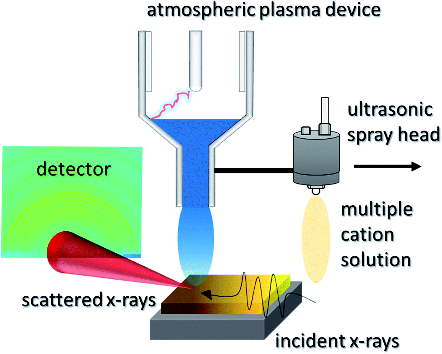 | ||
| Fig. 1 In situ wide angle X-ray scattering experimental configuration with rapid spray plasma processing. | ||
In situ wide angle X-ray scattering (WAXS)
In order to better understand the kinetics of perovskite formation, the RSPP setup was integrated into a beamline for in situ characterization with WAXS, which provides a means for probing the rapidly evolving crystalline species in RSPP perovskites. The in situ WAXS has a time resolution of 15 ms, which can effectively resolve the swift formation of the RSPP perovskite thin film. Intensity maps were obtained as the one in Fig. 2, where time is plotted against the scattering vector q between 0.3 Å−1 and 4.25 Å−1 to track the evolution of crystalline phases from the precursor materials. These maps were obtained for different mole fractions of cesium, 0.05 ≤ x ≤ 0.25, each condition for which was run in triplicate and observed to be self-consistent (Fig. S1†). | ||
| Fig. 2 Representative waterfall plot produced from wide angle X-ray scattering showing 2D intensity plotted over time. | ||
The (110) crystallographic plane resides around 1.0 Å−1 and serves as a good proxy for measuring perovskite crystallization. For all compositions measured, complete conversion to the final perovskite phase occurred within a few tens of milliseconds. A transient feature at ∼0.83 Å−1 appeared for each of the compositions. This feature appears at a lower q-value than is expected for PbI2 or PbBr2, and can therefore not be attributed to any of these species.25Fig. 3 shows normalized integrated intensity versus time plots obtained from the maps, comparing the (110) and transient intermediate intensities. At low cesium fractions, the growth of the intermediate crystalline phase preceded the formation of the perovskite crystal structure. However, the signal for the intermediate quickly grows and dissipates during the plasma exposure.
 | ||
| Fig. 3 Integrated intensity of (110) perovskite peak vs. time along with transient intermediate for different mole fractions of Cs for CsxFA1−xPb(I.17Br.83)3 with (a) x = 0.05, (b) x = 0.15, and (c) x = 0.25 produced with RSPP. | ||
Increasing x to 0.15 led to a decrease in the normalized intensity of the intermediate, while films with x = 0.25 suppressed the phase almost entirely. The mechanism for this decrease in intermediate phase with higher cesium content is likely related to accelerated film conversion. Previous work characterized that perovskite compositions with higher cesium content led to more rapid film conversion as observed by in situ absorbance measurements.9 In addition, methylammonium was also found to decrease the prominence of the intermediate phase, although to a lesser degree than cesium (Fig. S2†). The cause of the intermediate phase in multiple cation perovskite films appears to be linked to higher concentration of formamidinium, which makes the intermediate phase thermodynamically favorable in the short time scales preceding formation of the final perovskite crystal structure.
The rate of crystallization, G, was largely similar with cation composition (Fig. S3–S7†), an effect that was expected due to the partition of the plasma energy into primarily solvent removal. At the same nominal concentrations, the cation composition has little effect on G. Fig. 3a shows that the formation of the intermediate phase causes a small delay in perovskite crystallization for lower cesium content, but the (110) peak is fully formed within 500 ms for all compositions. Our previous work characterizing MAPbI3 films produced with RSPP showed the perovskite crystallization kinetics differed from classical thermal annealing processes.16 Here, we reiterate the classic Avrami approach in order to determine that the fast crystallization cannot be solely ascribed to temperature alone (Fig. S7†). This is apparent from the deviation from Arrhenius behavior (G ∼ 1/T), and is similar to RSPP single cation perovskite films. The conclusion of this and previous observations regarding a wide range of RSPP perovskite compositions is that reactive plasma species and UV photons contribute to accelerated growth rates by providing additional photo and chemical energy to cure the perovskite film. This is not unlike previous results using UV-enhanced crystallization.26
Film morphology and optoelectronic properties
The morphology of perovskite materials has been shown to be related to both processing methodology27,28 and film composition.29 To understand the influence of cation composition on RSPP perovskite, top-down scanning electron microscopy (SEM) images used to characterize film microstructure are shown in Fig. 4. The grain size distribution was extracted (Fig. S8a†), and mirroring the results found by others for conventional methodologies,30 the grain size increased with both the addition of cesium and methylammonium (Fig. S8b†). It is interesting to note that these multiple cation, mixed halide perovskites are more monodisperse than the RSPP single cation, MAPbI3 films we previously reported on ref. 16. The most striking difference in crystallization between the single and multiple cation RSPP perovskites is the presence of the transient intermediate phase in the latter. | ||
| Fig. 4 Top-down scanning electron micrographs of perovskite films with (a) x = 0.05, (b) x = 0.15, and (c) x = 0.25 produced with RSPP. | ||
Steady-state photoluminescence was performed to determine photostability of RSPP perovskite films as a function of cesium content. Fig. 5 shows normalized photoluminescence plots for the x = 0.05, x = 0.15, and x = 0.25 perovskites, where trends of increasing band gap and reduced phase separation with higher cesium content are both clearly evident. Higher Cs content reduced the higher energy shoulder (shaded in blue in Fig. 5) associated with bromine-rich regions that characterizes the Hoke effect31 compared to the main, iodide-rich peak (shaded in cyan in Fig. 5). The ratio between the higher energy and main peaks reduced from 0.21 for x = 0.05 to 0.11 for x = 0.15 to 0.05 for x = 0.25. The improved photostability for higher Cs content correlates with reduced intermediate phase, but is not caused by the change in film formation. In agreement with previous work,32 we confirm that it is indeed desirable to have slightly more Cs than Br, percentage-wise, in this compositional space of wide band gap perovskites.
 | ||
| Fig. 5 Steady-state photoluminescence plots for (a) x = 0.05, (b) x = 0.15, and (c) x = 0.25 produced with RSPP. Shaded areas illustrate the amount of phase separation between iodide-rich (cyan) and bromide-rich (blue) regions, where a higher concentration of Cs improves photostability and band gap. | ||
The complex refractive index (n + iκ) of perovskite thin films have been shown to be affected by cation composition, halide composition, and processing environment.33,34 The values of n and κ calculated from spectroscopic ellipsometry are useful in the modeling and optimization of complex module or tandem architectures and are therefore suitable as materials selection criteria.35 We used an effective medium theory to account for the observed phase segregation through the addition of a fourth oscillator term.36 As the degree of phase separation cannot be accounted for by the precursor stoichiometry, the normalized height of the iodide-rich and bromine-rich photoluminescence regions were taken as the nominal compositional weighting. The fit quality was adequate in all cases, with Χ2 < 2 observed for all the double cation perovskite films. Both the refractive index and extinction coefficient are shown in Fig. 6a and b. In agreement with others,37 the real part of the refractive index decreased with increasing cesium fraction.
 | ||
| Fig. 6 Calculated (a) refractive index, (b) extinction coefficient, and the (c) real and (d) imaginary parts of the dielectric function measured with spectroscopic ellipsometry for x = 0.05, 0.15, and 0.25 produced with RSPP. | ||
In ionic crystals such as these, a lower band-gap leads to a stronger dielectric response and thus a higher refractive index. The strength of the oscillator (fj) increased with increasing cesium, likely due to decreased phase segregation and therefore a larger volume of the iodide-rich material. The real (εr) and imaginary  part of the dielectric response can be calculated if the refractive index and extinction coefficient are known. The real and imaginary part of the dielectric function is shown in Fig. 6c and d. In a similar manner to the refractive index, εr decreased with increasing Cs fraction, while
  increased. If we consider a HTL such as NiO, reflection losses can be minimized at this interface by increasing the cesium fraction and decreasing the refractive index. The calculated absorption is also stronger for increased cesium fractions.
Based on this observation, we tested photostability under full illumination for p–i–n perovskite solar cells with x = 0.25 deposited with RSPP on top of PEDOT:PSS and with C60/BCP/Ag evaporated as the top device contacts. Fig. S9a† plots the maximum-power point of the device continuously tracked while aged in ambient air without any cooling (35 °C, 45% RH). The device exhibited no signs of degradation and actually improved in PCE by 12.5% after 12 h of testing. Future studies will test longer-term exposures, but this preliminary result indicates promising device stability. Future work will need to focus on improving performance and determining the correlation between intermediate phase and device performance since time constraints at the beamline limited process optimization and the champion device was 10% PCE (Fig. S9b†), although the Voc of 1.08 V is notably higher than any spin-coated device using the same architecture.
Mechanical properties: residual stress
Perovskite films have recently been shown to exhibit high values of residual film stress (>50 MPa)9 upon cooling to room temperature after annealing; the substrate constrains the perovskite, which has a CTE that is an order of magnitude larger than glass, from shrinking to its equilibrium distance. Importantly, the film stress is directly correlated to the formation temperature of the perovskite,11 which is usually at or above 100 °C during conventional processing. As discussed in previous work,16 plasma reactive species and UV photons contribute a non-negligible amount of energy to perovskite formation, lowering the gas temperature needed to completely cure the solution. Another major advantage of RSPP is the fast processing time, which was shown from the rapid crystallization observed during in situ WAXS. As a result, this method reduces the thermal load needed to form the perovskite, and thus we posited that the rapid curing would result in lower film stresses for RSPP perovskites.Film stress measurements were obtained using the substrate curvature method—a thin-film technique used to determine residual stresses in a variety of materials ranging from human skin38 to metal gridlines39—where a laser scans across the center of the substrate and the deflection is measured to determine the radius of curvature. Fig. 7 shows the measured film stress for CsxFA1−xPb(Br0.17I0.83)3 films for x = 0.05, 0.15, and 0.25. The plasma duty cycle is a convenient parameter for making fine adjustments to the energy conveyed by the plasma by truncating the input DC waveform at some fraction of its period. Here, the duty cycle was either 15% or 50%.
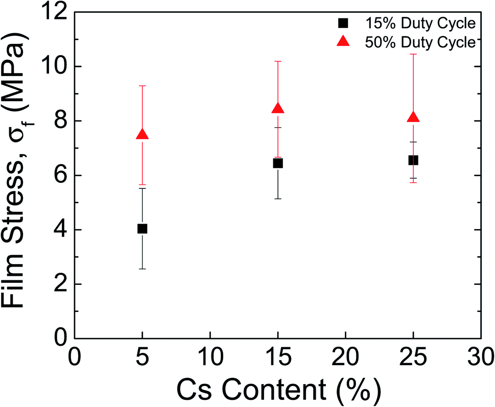 | ||
| Fig. 7 Measured perovskite film stress for x = 0.05, 0.15, and 0.25 produced with RSPP. The plasma duty cycle—or time between pulses—was varied at either 15% or 50%. In all cases, the tensile stress values are significantly lower than the previously measured stresses of 49.3 ± 3.2 MPa for x = 0.17 that was spin coated and formed at 100 °C. | ||
At 15% duty cycle, the measured stress values were 4.0 ± 1.5 MPa for x = 0.05, 6.4 ± 1.3 MPa for x = 0.15, and 6.6 ± 0.7 MPa for x = 0.25, while at 50% duty cycle, the measured stress values increased to 7.5 ± 1.8 MPa for x = 0.05, 8.4 ± 1.8 MPa for x = 0.15, and 8.1 ± 2.4 MPa for x = 0.25. Across all cesium contents, a lower duty cycle led to reduced film stresses, an expected result since the intensity and flux of plasma reactive species are reduced with lower duty cycle. Additionally, the low cesium content was observed to have the lowest film stress—an effect which could be attributed to the presence of the intermediate peak during formation—leading to less heat being coupled to the substrate. The significant reduction or absence of the intermediate phase for x = 0.15 and x = 0.25 result in relatively similar curing kinetics and comparable stress values.
Regardless of the formulation, however, the tensile stress values are about an order of magnitude lower than the previously measured stresses of 49.3 ± 3.2 MPa in identical double cation compositions that were spin coated and formed at 100 °C.11 The significantly reduced stresses for RSPP perovskites indicate superior thermomechanical reliability and higher resistance to fracture—a result which was previously documented in RSPP MAPbI3 films.16 Higher tensile stress values have also been correlated with decreased stability to environmental stressors.11
Conclusions
We have demonstrated an open-air process for depositing photostable, multiple cation perovskite compositions with the aim of improving reliability of this thin film technology. Cation composition is critical in the RSPP of metal halide perovskite materials as a means for tuning both the morphology and optoelectronic performance. The high flux of X-rays provided by the synchrotron light source enabled the observation of a transient intermediate crystalline phase during the formation of the perovskites, which decreased in prominence with increasing cesium fractions. Increasing the cesium or methylammonium fraction also led to larger grain diameters and decreased phase segregation. The observed phase segregation was considered in an ellipsometric model, and the refractive index, extinction coefficient, and complex dielectric response were calculated. The phase separation did not markedly impact the refractive index throughout most of the visible spectrum; however, the optical dispersion strongly depended on cation composition. The refractive index decreased and the extinction coefficient increased with increasing cesium fraction.Low residual stresses (<10 MPa) were observed for RSPP multiple cation, mixed halide perovskites for a range of cesium fractions. Devices made with RSPP multiple cation perovskites displayed high open-circuit voltages and good photostability. We plan to further optimize the spraying condition and plasma exposure to improve fill factors and short-circuit currents. In addition to highlighting a scalable and open-air method for perovskite deposition, we provided a formalism to measure transient crystalline phases in fast metal halide perovskite deposition methods.
Experimental methods
Perovskite precursors
The perovskite precursor solution consisted of methylammonium iodide (MAI), formamidinium iodide (FAI) (Dyesol), cesium iodide (CsI) (Sigma), and lead iodide (PbI2) and lead bromide (PbBr2) (TCI). All solvents were anhydrous and used as received (Acros). The preparation of the perovskite solution was performed by dissolving CsI, FAI, PbI2, and PbBr2 (MAI was included for the triple cation formulation) in anhydrous N,N-dimethylformamide (DMF, anhydrous, 99.8%) at a total concentration of 0.8 M. The solution was stirred and filtered before use.Rapid spray plasma process
The RSPP configuration used a blown arc discharge that was produced between two coaxial electrodes and blown out of a nozzle by the main process gas flow—in this case clean, dry air—at a flow rate of 35 standard liters per minute (slm). The high-voltage electrode was driven by a DC power supply at an excitation frequency of 21 kHz. The resulting arc current was 18.0 A. Briefly, the deposited liquid layers were exposed (250 ms) to the atmospheric plasma device to promote the curing of the sprayed solution. The substrates were placed at a vertical distance 4.0 cm from the plasma nozzle. The spray nozzle-to-substrate vertical distance and the plasma nozzle-to-spray nozzle horizontal distance were kept at a distance of 6 cm and 8 cm, respectively. The moving speed of the nozzles was kept constant at 4 cm s−1 and one pass was performed.In situ wide angle X-ray scattering
The measurements were made at the Stanford Synchrotron Radiation Lightsource (SSRL, Beamline 10-2). The RSPP was integrated into the beamline, such that the X-rays scattered orthogonal to the cure direction (Fig. 1a). An X-ray energy of 12.7 keV, an exposure time of 10 ms per frame and a shutter time of 5 ms resulted in a total exposure period of 15 ms. The RSPP system was assembled in Beamline 10-2. LaB6 was used to calibrate peak positions. The incident angle was 3°; a Pilatus 100 K detector was placed 23 cm from the sample; q-space between 0.3 Å−1 and 4.25 Å−1 was probed.Film stress measurements
Measurements to determine film stress were taken on the back-side of double side polished Si wafers in order to ensure enough reflected intensity from the surface of the substrate after depositing the perovskite. The thin film stress, σf, was then approximated by Stoney's equation:40 | (1) |
Device fabrication
ITO-coated glass (Xin Yan, 10 Ω □−1) was cleaned by successively sonicating in Extran detergent diluted 1![[thin space (1/6-em)]](https://www.rsc.org/images/entities/char_2009.gif) :10 in DI water, pure DI water, acetone, and isopropanol for 10 minutes each before being placed in a UV-ozone chamber for 15 min. PEDOT:PSS in water (Clevios Al 4083) was spin coated at 4000 rpm on the substrates. RSPP was performed to fabricate the perovskite layer without any additional annealing or post-treatments. 45 nm C60 (MER Corporation)/7.5 nm BCP (TCI)/Ag was then evaporated (Angstrom Amod)—the latter of which was deposited through a shadow mask—with a base pressure < 2 × 10⁻⁶ Torr in all cases.
:10 in DI water, pure DI water, acetone, and isopropanol for 10 minutes each before being placed in a UV-ozone chamber for 15 min. PEDOT:PSS in water (Clevios Al 4083) was spin coated at 4000 rpm on the substrates. RSPP was performed to fabricate the perovskite layer without any additional annealing or post-treatments. 45 nm C60 (MER Corporation)/7.5 nm BCP (TCI)/Ag was then evaporated (Angstrom Amod)—the latter of which was deposited through a shadow mask—with a base pressure < 2 × 10⁻⁶ Torr in all cases.
Perovskite characterization
Steady-state photoluminescence was measured using a spectrograph (Acton Research SpectraPro 500i) equipped with a Hamamatsu silicon CCD array detector. The materials were excited with the 457 nm line of an argon ion laser.Current–voltage measurements were performed using a Keithley model 2400 digital source meter and 300 W xenon lamp (Oriel) solar simulator was used for irradiation. The lamp was calibrated with an NREL-calibrated KG5 filtered Si reference cell. J–V curves were taken over an active area of 0.2 cm2 from forward to reverse bias sampled at 0.05 V intervals with a 0.1 s delay time at each voltage step before taking data. Maximum power point tracking was performed every 1 s using a perturb and measure software with a voltage step of 0.005 V to continuously track power output.
SEM was performed on a FEI Magellan 400 XHR FE-SEM. Prior to SEM observations, the device samples were coated with 5 nm of Au/Pd (60:40 ratio) to prevent image charging and distortion. ImageJ was used for image processing to determine the grain size distribution. SEM images were imported into the software and contrast tuned to enhance the visibility of grain boundaries. The Particle Size Distribution plugin was then utilized to calculate the grain sizes for each perovskite composition.
Spectral ellipsometry (SE) (Horiba Jobin UVISEL) was used to determine both the refractive index and extinction coefficients of the films. Measurements were fitted with a new amorphous dispersion model, containing up to 4 oscillator terms to account for the phase segregation observed in the mixed-bromide perovskites.
Conflicts of interest
There are no conflicts to declare.Acknowledgements
This material is based upon work supported by the U.S. Department of Energy's Office of Energy Efficiency and Renewable Energy (EERE) under Solar Energy Technologies Office (SETO) Agreement Number DE-EE0008559. Part of this work was performed at the Stanford Nano Shared Facilities (SNSF), supported by the National Science Foundation under award ECCS-1542152. Additional support was provided by the National Science Foundation Graduate Research Fellowship, awarded to N. Rolston under award DGE-1656518. Use of the Stanford Synchrotron Radiation Lightsource SLAC National Accelerator Laboratory, is supported by the U.S. Department of Energy, Office of Science, Office of Basic Energy Sciences under Contract No. DE-AC02-76SF00515. We also thank Ron Marks for helpful discussions and experimental assistance at Beamline 10-2 at SSRL.References
- W. S. Yang, B.-W. Park, E. H. Jung, N. J. Jeon, Y. C. Kim, D. U. Lee, S. S. Shin, J. Seo, E. K. Kim, J. H. Noh and S. Il Seok, Science, 2017, 356, 1376–1379 CrossRef CAS.
- D. Bryant, N. Aristidou, S. Pont, I. Sanchez-Molina, T. Chotchunangatchaval, S. Wheeler, J. R. Durrant and S. A. Haque, Energy Environ. Sci., 2016, 9, 1655–1660 RSC.
- X. Zhao, H.-S. Kim, J.-Y. Seo and N.-G. Park, ACS Appl. Mater. Interfaces, 2017, 9, 7148–7153 CrossRef CAS.
- B. Conings, J. Drijkoningen, N. Gauquelin, A. Babayigit, J. D'Haen, L. D'Olieslaeger, A. Ethirajan, J. Verbeeck, J. Manca, E. Mosconi, F. De Angelis and H. G. Boyen, Adv. Energy Mater., 2015, 5, 1500477 CrossRef.
- Q. Wang, B. Chen, Y. Liu, Y. Deng, Y. Bai, Q. Dong and J. Huang, Energy Environ. Sci., 2017, 10, 516–522 RSC.
- N. Rolston, A. D. Printz, J. M. Tracy, H. C. Weerasinghe, D. Vak, L. J. Haur, A. Priyadarshi, N. Mathews, D. J. Slotcavage, M. D. McGehee, R. E. Kalan, K. Zielinski, R. L. Grimm, H. Tsai, W. Nie, A. D. Mohite, S. Gholipour, M. Saliba, M. Grätzel and R. H. Dauskardt, Adv. Energy Mater., 2018, 8, 1702116 CrossRef.
- T. J. Jacobsson, L. J. Schwan, M. Ottosson, A. Hagfeldt and T. Edvinsson, Inorg. Chem., 2015, 54, 10678–10685 CrossRef CAS.
- C. Ramirez, S. K. Yadavalli, H. F. Garces, Y. Zhou and N. P. Padture, Scr. Mater., 2018, 150, 36–41 CrossRef CAS.
- K. A. Bush, N. Rolston, A. Gold-Parker, S. Manzoor, J. Hausele, Z. J. Yu, J. A. Raiford, R. Cheacharoen, Z. C. Holman, M. F. Toney, R. H. Dauskardt and M. D. McGehee, ACS Energy Lett., 2018, 1225–1232 CrossRef CAS.
- J. Zhao, Y. Deng, H. Wei, X. Zheng, Z. Yu, Y. Shao, J. E. Shield and J. Huang, Sci. Adv., 2017, 3, eaao5616 CrossRef.
- N. Rolston, K. A. Bush, A. D. Printz, A. Gold-Parker, Y. Ding, M. F. Toney, M. D. McGehee and R. H. Dauskardt, Adv. Energy Mater., 2018, 1802139 CrossRef.
- J. W. Hutchinson and Z. Suo, Adv. Appl. Mech., 1991, 29, 63–191 Search PubMed.
- W. Yoon and X. Huang, ECS Trans., 2010, 33, 907–911 CAS.
- H. Yonezu, I. Sakuma, T. Kamejima, M. Ueno, K. Nishida, Y. Nannichi and I. Hayashi, Appl. Phys. Lett., 1974, 24, 18–19 CrossRef CAS.
- W. K. Busfield and P. Taba, Polym. Degrad. Stab., 1996, 51, 185–196 CrossRef CAS.
- F. Hilt, M. Q. Hovish, N. Rolston, K. Brüning, C. J. Tassone and R. H. Dauskardt, Energy Environ. Sci., 2018, 11, 2102–2113 RSC.
- B. L. Watson, N. Rolston, A. D. Printz and R. H. Dauskardt, Energy Environ. Sci., 2017, 10, 2500–2508 RSC.
- S. Dong, M. Watanabe and R. H. Dauskardt, Adv. Funct. Mater., 2014, 24, 3075–3081 CrossRef CAS.
- M. Watanabe, L. Cui and R. H. Dauskardt, Org. Electron., 2014, 15, 775–784 CrossRef CAS.
- N. Rolston, A. D. Printz, F. Hilt, M. Q. Hovish, K. Brüning, C. J. Tassone and R. H. Dauskardt, J. Mater. Chem. A, 2017, 5, 22975–22983 RSC.
- J.-W. Lee, D.-H. Kim, H.-S. Kim, S.-W. Seo, S. M. Cho and N.-G. Park, Adv. Energy Mater., 2015, 5, 1501310 CrossRef.
- D. P. McMeekin, G. Sadoughi, W. Rehman, G. E. Eperon, M. Saliba, M. T. Horantner, A. Haghighirad, N. Sakai, L. Korte, B. Rech, M. B. Johnston, L. M. Herz and H. J. Snaith, Science, 2016, 351, 151–155 CrossRef CAS.
- W. Tan, A. R. Bowring, A. C. Meng, M. D. McGehee and P. C. McIntyre, ACS Appl. Mater. Interfaces, 2018, 10, 5485–5491 CrossRef CAS.
- M. Saliba, T. Matsui, J.-Y. Seo, K. Domanski, J.-P. Correa-Baena, M. K. Nazeeruddin, S. M. Zakeeruddin, W. Tress, A. Abate, A. Hagfeldt and M. Grätzel, Energy Environ. Sci., 2016, 9, 1989–1997 RSC.
- J. Schlipf, P. Docampo, C. J. Schaffer, V. Körstgens, L. Bießmann, F. Hanusch, N. Giesbrecht, S. Bernstorff, T. Bein and P. Müller-Buschbaum, J. Phys. Chem. Lett., 2015, 6, 1265–1269 CrossRef CAS.
- S. J. Park, A. R. Kim, J. T. Hong, J. Y. Park, S. Lee and Y. H. Ahn, J. Phys. Chem. Lett., 2017, 8, 401–406 CrossRef CAS.
- W. Nie, H. Tsai, R. Asadpour, J.-C. Blancon, A. J. Neukirch, G. Gupta, J. J. Crochet, M. Chhowalla, S. Tretiak, M. A. Alam, H.-L. Wang and A. D. Mohite, Science, 2015, 347, 522–525 CrossRef CAS.
- X. Li, D. Bi, C. Yi, J.-D. Decoppet, J. Luo, S. M. Zakeeruddin, A. Hagfeldt and M. Gratzel, Science, 2016, 353, 58–62 CrossRef CAS.
- M. Hu, C. Bi, Y. Yuan, Y. Bai and J. Huang, Adv. Sci., 2015, 3, 1500301 CrossRef.
- W. Rehman, D. P. McMeekin, J. B. Patel, R. L. Milot, M. B. Johnston, H. J. Snaith and L. M. Herz, Energy Environ. Sci., 2017, 10, 361–369 RSC.
- E. T. Hoke, D. J. Slotcavage, E. R. Dohner, A. R. Bowring, H. I. Karunadasa and M. D. McGehee, Chem. Sci., 2015, 6, 613–617 RSC.
- K. A. Bush, K. Frohna, R. Prasanna, R. E. Beal, T. Leijtens, S. A. Swifter and M. D. McGehee, ACS Energy Lett., 2018, 3, 428–435 CrossRef CAS.
- P. Löper, M. Stuckelberger, B. Niesen, J. Werner, M. Filipič, S.-J. Moon, J.-H. Yum, M. Topič, S. De Wolf and C. Ballif, J. Phys. Chem. Lett., 2015, 6, 66–71 CrossRef.
- J. Werner, G. Nogay, F. Sahli, T. C.-J. Yang, M. Bräuninger, G. Christmann, A. Walter, B. A. Kamino, P. Fiala, P. Löper, S. Nicolay, Q. Jeangros, B. Niesen and C. Ballif, ACS Energy Lett., 2018, 3, 742–747 CrossRef CAS.
- S. Manzoor, Z. J. Yu, A. Ali, W. Ali, K. A. Bush, A. F. Palmstrom, S. F. Bent, M. D. Mcgehee and Z. C. Holman, Sol. Energy Mater. Sol. Cells, 2017, 1–7 Search PubMed.
- D. A. G. Bruggeman, Ann. Phys., 1935, 416, 636–664 CrossRef.
- P. F. Ndione, Z. Li and K. Zhu, J. Mater. Chem. C, 2016, 4, 7775–7782 RSC.
- K. Levi, R. J. Weber, J. Q. Do and R. H. Dauskardt, Int. J. Cosmet. Sci., 2010, 32, 276–293 CrossRef CAS.
- R. E. Brock, P. Hebert, J. Ermer and R. H. Dauskardt, Sol. Energy Mater. Sol. Cells, 2018, 179, 178–184 CrossRef CAS.
- G. G. Stoney, Proc. R. Soc. London, Ser. A, 1909, 82, 172–175 CrossRef CAS.
Footnote |
| † Electronic supplementary information (ESI) available. See DOI: 10.1039/c9ta07980g |
| This journal is © The Royal Society of Chemistry 2020 |